

HIT 2SC454 Datasheet
Application
High frequency amplifier, mixer
Outline
TO-92 (2)
2SC454
Silicon NPN Epitaxial
1. Emitter
2. Collector
3. Base
3
2
1

2SC454
Absolute Maximum Ratings (Ta = 25°C)
Item Symbol Ratings Unit
Collector to base voltage V
Collector to emitter voltage V
Emitter to base voltage V
Collector current I
Collector power dissipation P
CBO
CEO
EBO
C
C
Junction temperature Tj 150 °C
Storage temperature Tstg –55 to +150 °C
Electrical Characteristics (Ta = 25°C)
Item Symbol Min Typ Max Unit Test conditions
Collector to base breakdown
V
(BR)CBO
voltage
Collector to emitter breakdown
V
(BR)CEO
voltage
Emitter to base breakdown
V
(BR)EBO
voltage
Collector cutoff current I
Emitter cutoff current I
CBO
EBO
DC current transfer ratio hFE*
Base to emitter voltage V
Collector to emitter saturation
V
BE
CE(sat)
voltage
Gain bandwidth product f
T
Collector output capacitance Cob — — 3.5 pF VCB = 10 V, IE = 0, f = 1 MHz
Noise figure NF — — 25 dB VCE = 6 V, IC = 0.1 mA,
IF power gain IFG — 35 — dB VCE = 12 V, IC = 1 mA,
Note: 1. The 2SC454 is grouped by hFE as follows.
BCD
100 to 200 160 to 320 250 to 500
30 — — V IC = 10 µA, IE = 0
30 — — V IC = 1 mA, RBE = ∞
5——VI
— — 0.5 µAV
— — 0.5 µAV
1
100 — 500 V
— 0.63 0.75 V VCE = 12 V, IC = 2 mA
— — 0.2 V IC = 10 mA, IB = 1 mA
— 230 — MHz VCE = 12 V, IC = 2 mA
30 V
30 V
5V
100 mA
200 mW
= 10 µA, IC = 0
E
= 18 V, IE = 0
CB
= 2 V, IC = 0
EB
= 12 V, IC = 2 mA
CE
f = 1 kHz, R
f = 455 kHz, Rg
R
= 40 kΩ
L
= 500 Ω
g
= 1.5 kΩ,
2
2SC454
Small Signal y Parameters (VCE = 12 V, IC = 2mA, Emitter Common)
Item Symbol f 2SC454B 2SC454C Unit
Input admittance yie 455 kHz 0.35 + j0.074 0.28 + j0.070 mS
1MHz 0.35 + j0.130 0.28 + j0.125
Reverse transfer admittance yre 455 kHz –j0.005 –j0.005 mS
1MHz –j0.013 –j0.013
Forward transfer admittance yfe 455 kHz 66 – j2.43 64 – j2.60 mS
1MHz 66 – j4.27 66 – j5.7
Output admittance yoe 455 kHz 0.006 + j0.02 0.007 + j0.022 mS
1MHz 0.006 + j0.047 0.007 + j0.049
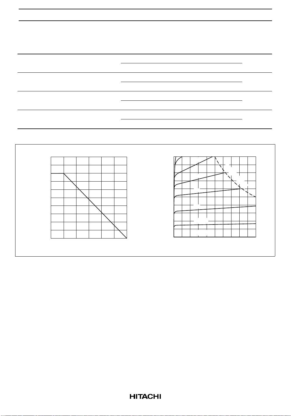
Maximum Collector Dissipation Curve
250
(mW)
200
C
150
100
50
Collector Power Dissipation P
0 50 100 150
Ambient Temperature Ta (°C)
Typical Output Characteristics (1)
20
16
(mA)
C
12
8
4
Collector current I
048121620
100
P
C
80
60
40
20 µA
IB = 0
Collector to Emitter Voltage V
= 200 mW
CE
(V)
3
 Loading...