

HIT 2SC1890A Datasheet
2SC1890, 2SC1890A
Silicon NPN Epitaxial
Application
• Low frequency high voltage amplifier
• Complementary pair with 2SA893/A
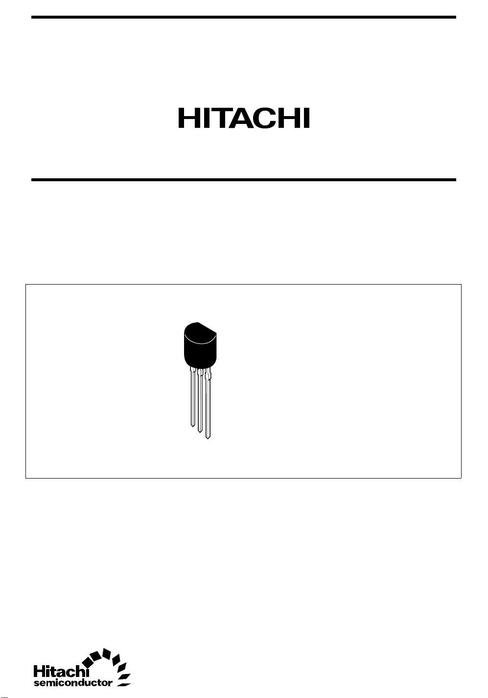
Outline
TO-92 (1)
1. Emitter
2. Collector
3. Base
3
2
1
2SC1890, 2SC1890A
Absolute Maximum Ratings (Ta = 25°C)
Ratings
Item Symbol 2SC1890 2SC1890A Unit
Collector to base voltage V
Collector to emitter voltage V
Emitter to base voltage V
Collector current I
Collector power dissipation P
CBO
CEO
EBO
C
C
Junction temperature Tj 150 150 °C
Storage temperature Tstg –55 to +150 –55 to +150 °C
Electrical Characteristics (Ta = 25°C)
2SC1890 2SC1890A
Item Symbol Min Typ Max Min Typ Max Unit Test conditions
Collector to emitter
breakdown voltage
Collector cutoff current I
DC current tarnsfer ratio hFE*
Base to emitter voltage V
Collector to emitter
saturation voltage
Gain bandwidth product f
Collector output
capacitance
Noise figure NF — 2 10 — 2 10 dB VCE = 6 V, IC = 50 µA,
Note: 1. The 2SC1890/A is grouped by hFE as follows.
V
(BR)CEO
CBO
90 — — 120 — — V IC = 1 mA, RBE = ∞
— — 0.5 — — — µAVCB = 75 V, IE = 0
—————0.5µAVCB = 100 V, IE = 0
1
250 — 1200 250 — 1200 VCE = 12 V, IC = 2 mA
— — 0.75 — — 0.75 V VCE = 12 V, IC = 2 mA
— — 0.5 — — 0.5 V IC = 10 mA, IB = 1 mA
— 200 — — 200 — MHz VCE = 12 V, IC = 2 mA
V
BE
CE(sat)
T
Cob — 1.6 — — 1.6 — pF VCB = 25 V, IE = 0,
90 120 V
90 120 V
55V
50 50 mA
300 300 mW
f = 1 MHz
R
= 50 kΩ, f = 1 kHz
g
DEF
250 to 500 400 to 800 600 to 1200
See characteristic curves of 2SC1775 and 2SC1775A.
2
 Loading...