

Page 1
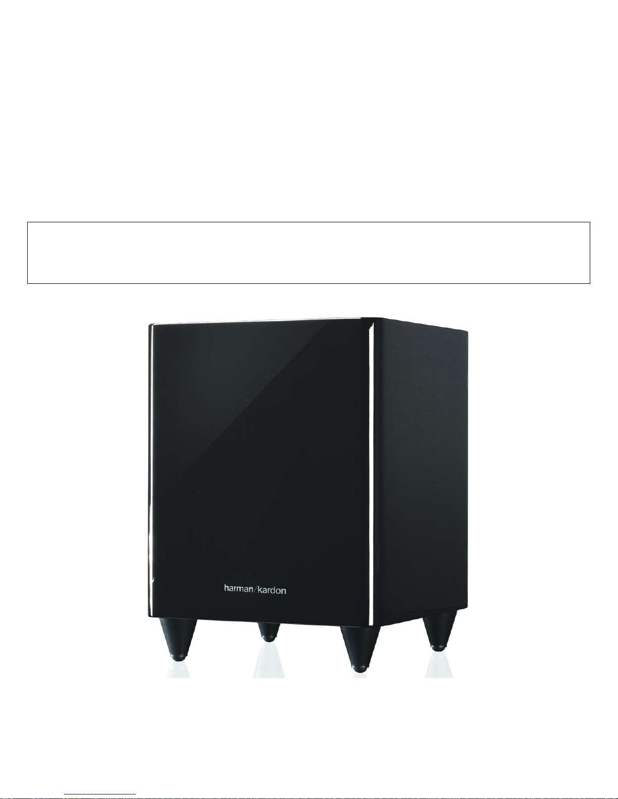
harman/kardon
HKTS 200 SUB
(HKTS 20/HKTS 30/HKTS 60 SUBWOOFER)
SERVICE MANUAL
harman/kardon, Inc.
8500 Balboa Blvd.
Released 2010 Northridge, CA. 91329 Rev1 3/2011
Discontinued XXXX
Page 2

HKTS200SUB harman/kardon
CONTENTS
BASIC SPECIFICATIONS . . . . . . . . . . . . ……………………………………. . . . 1
DETAILED SPECIFICATIONS. . . . . . . . . . . . . .. . . . . . . . . ………………….. …2
PACKAGING. . . . . . . . . . . . . .. . . . . . . …….………………… . . . . .. . .. . .. . . . . 4
CONTROLS . . . . . . . . . . . . . .. . . . . . . ……………………… . ………………….. 5
CONNECTIONS…………………………………….………..……. . . .. . .. . . . .. . .. 6
OPERATION……. . . . . .. . . . . . . . .. .. . . . .. .. . . . . ……………………………….9
BASIC TROUBLESHOOTING GUIDE . . . . . . . . …………..……………………...9
TEST PROCEDURE. . . . . . . . . . . …………………………………………………10
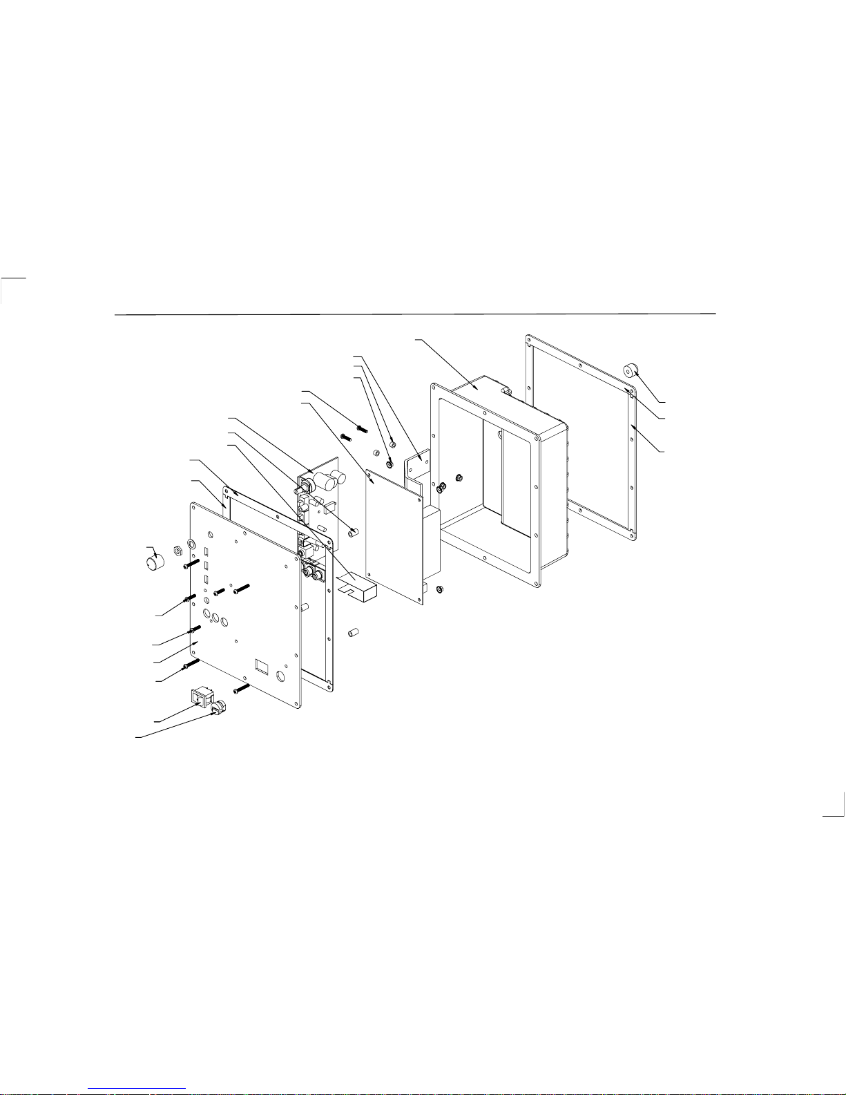
AMPLIFIER EXPLODED VIEW. . . . …………… ………. ………... . . .. .. ... . … . 11
UNIT EXPLODED VIEW. . . . …………… ……………. .. ………... . . .. .. ... . … . 12
BLOCK DIAGRAM . . . . . . . . . . . . . .. . . . . . . ……………… . . . . .. . .. . .. . . . . 13
PCB DRAWINGS. .. . . . . . . . . . . . . . .. . . . . ……… . …………. . . . .. .. .. . .. . . . 14
ELECTRICAL PARTS LIST …………. .... . .. . . . …………………………... … . . 17
SEMICONDUCTOR PINOUTS . . . .. .. .. .. . . . .. . ……………..………..………. .19
SCHEMATIC DIAGRAMS . . . . . . . . .. .. .. .. . . . .. . ………………………..……. .37
HKTS 200 SUB SPECIFICATIONS
Amplifier Power (RMS) 200 Watts
Driver 8" woofer, Sealed Enclosure
Inputs Stereo Line Level and dedicated Subwoofer (LFE)
Frequency Response 45Hz – 200Hz
External Trigger Input Voltage 3 ~ 30 volts AC/DC
Dimensions (H x W x D) 13-29/32" x 10-1/2" x 10-1/2"
(353mm x 267mm x 267mm)
Weight 19.8 lb (9kg)
Occasional refinements may be made to existing products without notice but will always meet or exceed original
specifications unless otherwise stated.
Page 3
r
ype (
)
p
)
e
r
z
r
P
P
t
p
.
y
y
t
t
n
n
e
(
)
V
r
V
p
e
K
s
Q
p
e
e
e
e
r
r
r
t
B
r
r
.
g
per
p
.
p
f
r
gg
t
g
g
n
)
p
g
)
)
p
y
p
.
f
.
t
p
t
s
pp
e
t
pp
e
t
pp
e
p
z
n
C
p
j
.
)
).
)
).
y
r
y
r
y
r
p
r
HKTS200SUB harman/kardon
2
HKTS200SUB Amplifier Specifications
Amplifier Section
T
Load Im
Rated Output Powe
THD @ Rated Powe
THD @ 1 Watt <0.2 % <0.4 AUX-0025 + AP DSP Audio Anlyzer + 20kHz L
DC Offse
Damping Factor >10 DF -
Input Sensitivit
Input Reference Frequenc
Input for 1 Watt Outpu
Gain (L, R and LFE inputs) 45 dB - RCA input to speaker output, Single input drive
Signal to Nois
SNR-A-Weighted 70 dBA 67.5
SNR-un-weighted 60 dB
Residual Noise Floor <1 mVrms -
Input Impedanc
Line Input 10
Filters & E
Am
Amplifier frequency respons
LP filter ~160 Hz - Fixed, 4th orde
HP Filte
LF Boos
AP Filte
Limite
Limiter Yes - - Digital limiter integral to audio processor IC
Maximum THD Under Limitin
Features
Volume Control Ta
Crossover Control No - - O
Phase Control 0/180 Deg. +/-10 2 position, 0 & 180
LF Boost Control Yes Functional 2
LED Indicato
Tri
ATO Control Yes - Functional 2 position, On & Auto
Input Confi
Line In (R / L
LFE In Yes - Functional RCA Jack, Pur
Si
Auto-Turn-On (yes/no
ATO In
ATO Line in
ATO Turn-on time <1 s Functional
Time to Turn Of
Ext. Trigger inpu
Activation Voltage >3 V Functional
Activation curren
Transients/Pop
ATO Transient <0.5 VTurn-on Transien
Turn-off Transien
Protections
Out
Output Over Current protectio
Output DC Protection Yes - Thermal Protection Yes NTC sensor ad
Mains Fuse Rating (120v
Mains Fuse Rating (230v
Efficienc
Efficiency at rated powe
Efficienc
Standb
Idle in
Paramete
Class AB, D, other
edance (speaker
lifier frequency respons
er Inpu
uratio
nal Sensing (ATO
ut test frequenc
ut level 1.5 mV Functional QA Test is 1mV verify amplifier is off, 2.5 mV verify amplifier turns on
ut Short Circuit Protection Yes - - Direct short between output terminal, recoverable @ 1 W, 50 H
at 1/8 of rated powe
Input powe
ut powe
Specification Unit QA Test Limits Test Conditions, Notes, and Comments
D - - No external heat sink required. Digital 192 kHz ternary mode PWM.
4 Ohm - Minimum rated load impedanc
200 W 200 50 H
<0.5 % <1 AUX-0025 + AP DSP Audio Anlyzer + 20kHz L
<25 mV <35
50 Hz - L, R or LFE Inpu
11.2 mVrms ±1dB RCA input to speaker output, Single input drive
Ohms - Applies to L, R or LFE Input
30-300 Hz +/-1dB QA limits are relative to reference respons
20-500 Hz +/-3dB QA limits are relative to reference respons
~40 Hz - Fixed, 6th orde
~50 Hz - Selectable, 2nd order parametric, +3 d
80 Hz - Crossover phase alignment.
5 % 7 QA tests THD at up to 15 dB into limiter.
LOG - Functional
Yes - Functional 2 state, Blue = On, Off = Off
Yes - Functional 3.5mm Mono Jack, Jack Sensin
Yes - Functional RCA Jacks, Red, White (Right and Left)
Yes Functional
50 Hz Functional
15 min Functional Time is measured by MCU, PV units measured 14 min
<3 mA Functional ~30k input impedance
<0.5 V<0.5 V-
12 A - Integral to power I
6.3 A slo-blo 250V, Internal Fuse, SMPS PCBA mounted (pigtail, soldered in place
5 A slo-blo 250V, Internal Fuse, SMPS PCBA mounted (pigtail, soldered in place
75 % 60 % -
0.8 W <1
8 W <10
Functional Speaker Output, Amplifier wake from standby, PV sample < 0.1 V, not audibl
Functional AC Line Connect, PV sample < 0.1 V, not audibl
Functional AC Line Disconnect, PV sample < 0.1 V, not audibl
Measured at amplifier board, damping factor dependant on H bridge Rdson + output filter
im
edance + SMPS, typically 0.1 + 0.2 + 0.05 Ohm
broad band noise from the ADC is present at the output but not audible
relative to 1W, AUX-0025 + AP DSP Audio Anlyzer + 20kHz LP + A-Weighting filter, PV
measured ~350 u
- relative to 1W, AUX-0025 + AP DSP Audio Anlyzer + 20kHz LP , PV measured 2m
Band-pass Measurement at Line freq.+ harmonics, AUX-0025 + 22K + 20 brick wall filters,
Line level in
Implemented using DSP
tional, 3-pin header on PCBA for future models
osition, On & Of
Designed to trigger from 3.3 - 30 V sources, AC or DC, QA test uses 3 V DC for fucntion
test. PV am
Detects shorts to ground or VCC on outputs (H-Bridge Failure), LED blinks rapidly, SMPS is
shut down to
Nominal Line voltage, Mains input to speaker outputs.
uts may be terminated using 1K Ohm
le
lifiers measured 2.9 V AC, 1.6 V DC.
revent, checks and attempts recovery every 20 seconds
acent power amplifier IC
Page 4
r
y
p.
d
p
y
y
t
y p
w
e
)
)
g
)
x
x
x
xOff0x1x
x
x
f
HKTS200SUB harman/kardon
3
Paramete
Power suppl
Type SMPS - -
Voltage Range
erating frequenc
O
Efficienc
Detachable AC power cord No - - Fixed Euro Plug for 220-240 V units, and fixed US plug for 100-120 V units
Standb
ower dra
Specification Unit QA Test Limits Test Conditions, Notes, and Comments
Half bridge, with auxiliary fly back standby supply.
1/2 rated power continuous, and rated power for > 1 Minute, 25 degree ambient, rated
220-240 or 100-
120
50-60 Hz >80% - - At rated power outpu
<0.5 W -
Vac 190 & 264
resistive load measured on bench to
IQC to test power supply at 264 V, 50 Hz input voltage, shall operate at +/- 10 % of the rate
values
ATO / Trigger Truth Tabl
Trigger Jack Sense
(1=jack, 0=no jack)
11
10
0
0
Trigger Input
State
(1 = high,
0=low
Power
Mode
(1=ON,
0=Auto
Input Signal
SW
01 On
00 Of
Sense
(1=signal, 0=no
nal
si
System State
On
On
Page 5
HKTS200SUB harman/kardon
4
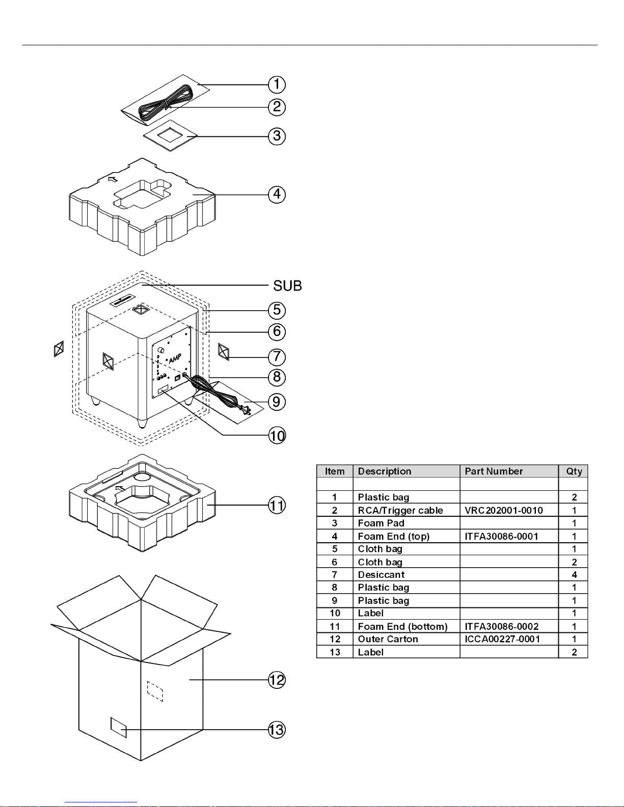
PACKAGING
Page 6
HKTS200SUB Rear-Panel Connections
PL0004-01001
1
2
3
4
5
8
9
6
7
HKTS200SUB harman/kardon
5
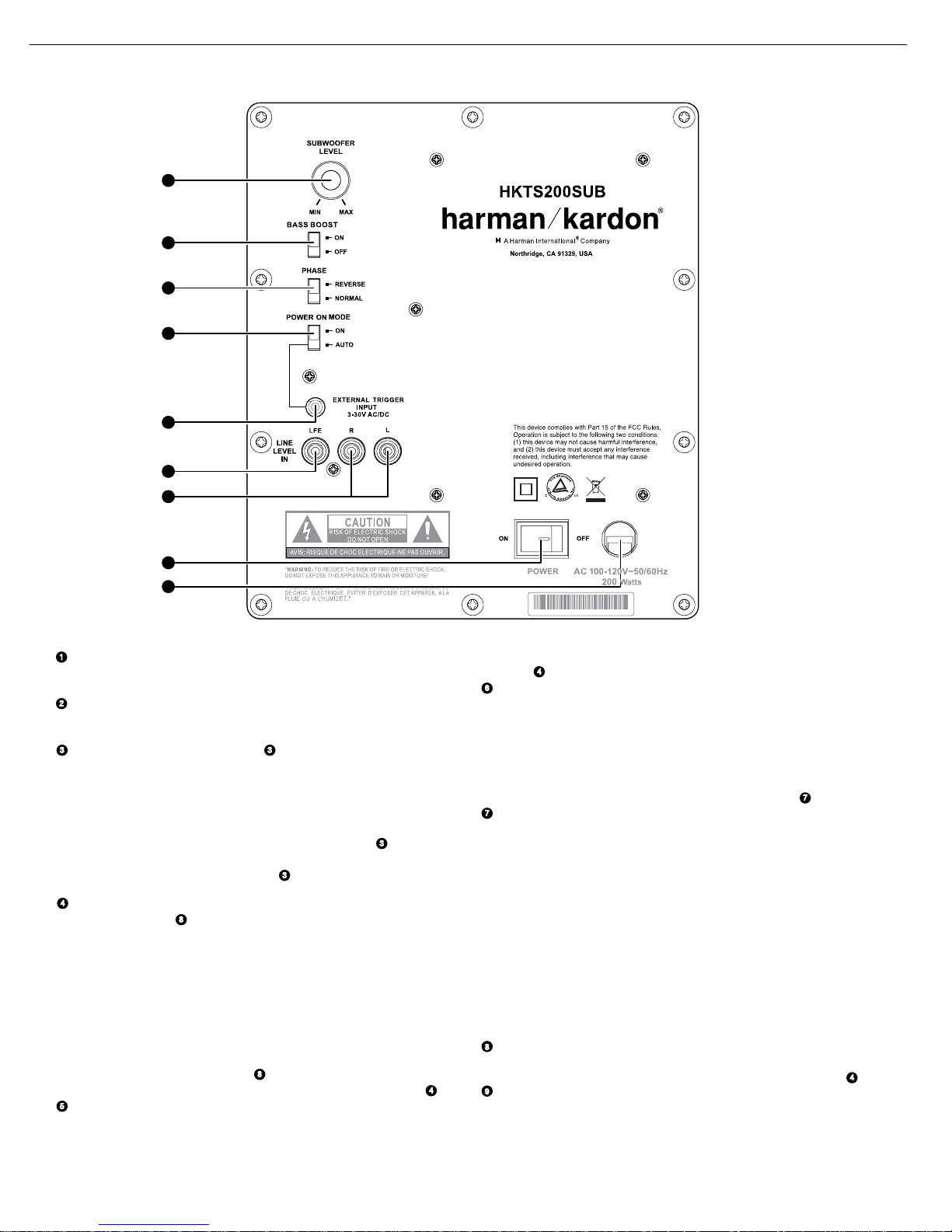
1
Subwoofer Level Control: Use this control to adjust the HKTS200SUB’s
volume. Turn clockwise to increase the volume; turn counterclockwise
to decrease the volume.
2
Bass Boost Switch: Set this switch to ON to enhance the
HKTS200SUB’s low-frequency performance. Set this switch to OFF
for normal low-frequency performance.
3 3
Phase Switch: The Phase Switch determines whether the
HKTS200SUB’s piston-like action moves in and out in phase with the
satellite speakers. If the subwoofer were to play out of phase with the
satellite speakers, the sound waves produced by the subwoofer could
be canceled out, reducing bass performance and sonic impact.
This phenomenon depends in part on the relative placement of all the
speakers in the room. In most cases the Phase Switch should be left
in the NORMAL position. However, it does no harm to experiment,
and you can leave the Phase Switch in the position that maximizes
bass response and impact.
4
Power On Mode Switch: When set in the AUTO position and when
the Power Switch is set to ON, the HKTS200SUB will automatically
8
3
turn itself on when it receives an audio signal, and will enter the
standby mode once no audio signal has been received for about
15 minutes. When this switch is set in the ON position,
the HKTS200SUB will remain on whether or not it is receiving an
audio signal.
An LED on the HKTS200SUB’s top panel indicates whether the
subwoofer is in the on or standby state:
• When the LED is illuminated white, the HKTS200SUB is turned on.
• When the LED is not illuminated, the HKTS200SUB is in standby mode.
When the Master Power Switch is set to OFF, the LED will not be
illuminated, no matter what setting the Power On Mode Switch is in.
5
External Trigger Input: Use the mini-plug of the supplied combination
8
LFE and trigger cable to connect the External Trigger Input to the
trigger output of another compatible component. Whenever a trigger
signal between 3 and 30V (AC or DC) is detected, the HKTS200SUB’s
amplifier will turn on. The HKTS200SUB’s amplifier will turn off after
3
4
the trigger signal ceases.
Switch is in the AUTO position.)
6
Line-Level LFE In Connector: Use the LFE (purple) connector of the
4
(This will occur even when the Power On Mode
supplied combination LFE and trigger cable to connect the Line-Level
LFE In to the dedicated subwoofer output of a receiver or preamp/
processor. This input bypasses the HKTS200SUB’s internal crossover
circuitry, so it should only be used with a subwoofer output that has
been low-pass filtered. If your receiver or preamp/processor does not
have a dedicated subwoofer output that is low-pass filtered you should
use the HKTS200SUB’s Line-Level L/R In Connectors instead.
7
Line-Level L/R In Connectors: Use these connectors if your receiver or
7
preamp/processor does not have digital surround sound decoding or a
subwoofer output that is low-pass filtered.
• If your receiver or preamp/processor has a separate subwoofer
output, use the LFE (purple) connector of the supplied combination
LFE and trigger cable to connect it to either one of the HKTS200SUB’s
Line-Level L/R In Connectors.
• If your receiver or preamp/processor does not have a separate
subwoofer output, use two Y-adapters (not supplied). Connect an
adapter’s single end to the unit’s preamp output for that channel.
Connect one of the adapter’s dual ends to the main amp input for that
channel, and connect the adapter’s other dual end to one of the
HKTS200SUB’s Line-Level L/R In Connectors. Repeat with the other
Y-adapter, preamp channel, main amp input and HKTS200SUB
Line-Level L/R In Connector.
8
Power Switch: Set this switch in the ON position to turn the
HKTS200SUB on. The subwoofer will then either be on or in standby
mode, depending on the setting of the Power On Mode Switch .
9
Power Cord (Non-Detachable): After you have made and verified all
4
subwoofer and speaker connections described in this manual, plug this
cord into an active, unswitched electrical outlet for proper operation of
the HKTS200SUB. DO NOT plug this cord into the accessory outlets
found in some audio components.
Page 7
+–
+– +–
+–+–
LEFT
SUB
LFE OUT
+– +–
+ –
+–
+ –
+–
+ –
RIGHT
SURROUNDFRONT CENTER
Left Front Right Front
Left
Surround
Right
Surround
Center
Subwoofer
Receiver
LFE/Trigger Cable
(Purple Ends)
Surround Left
Speaker Cable
(Blue Bands)
Front Left
Speaker Cable
(White Bands)
Front Right
Speaker Cable
(Red Bands)
Center
Speaker Cable
(Green Bands)
Surround Right
Speaker Cable
(Gray Bands)
HKTS200SUB harman/kardon
6
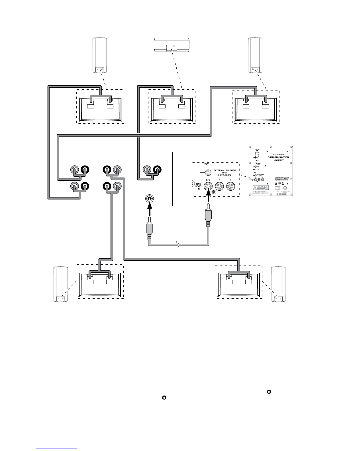
Connecting the Subwoofer to a Receiver or
Preamp/Processor With a Dedicated Subwoofer Output
Use this installation method for receivers and preamp/processors that
have a dedicated subwoofer output with low-pass filtering (also called
bass management). If the dedicated subwoofer output does not have
low-pass filtering, follow the instructions in Connecting the Subwoofer
to a Receiver or Preamp/Processor With Line Outputs, on page 9.
Use the LFE (purple) connector of the supplied combination LFE and
trigger cable to connect the HKTS200SUB’s Line-Level LFE In Jack
to the dedicated subwoofer output (or LFE output) of your receiver or
preamp /processor.
Connect each satellite speaker and the center speaker to the
corresponding speaker terminals on your receiver or amplifier.
In your receiver or preamp/processor’s setup menu, configure it for
Subwoofer ON, and set the front left, front right, center, and surround
speakers to Small. After you have made and verified all connections,
plug the HKTS200SUB’s AC Power Cord into an active AC outlet.
6
9
Page 8
+–
+– +–
+–+–
LEFT
LINE-LEVEL
OUTPUTS
LR
+– +–
+ –
+–
+ –
+–
+ –
RIGHT
SURROUNDFRONT CENTER
Left Front Right Front
Left
Surround
Right
Surround
Center
Subwoofer
Receiver
RCA Cable
(Not Supplied)
(Red and White Ends)
Surround Left
Speaker Cable
(Blue Bands)
Front Left
Speaker Cable
(White Bands)
Front Right
Speaker Cable
(Red Bands)
Center
Speaker Cable
(Green Bands)
Surround Right
Speaker Cable
(Gray Bands)
HKTS200SUB harman/kardon
7
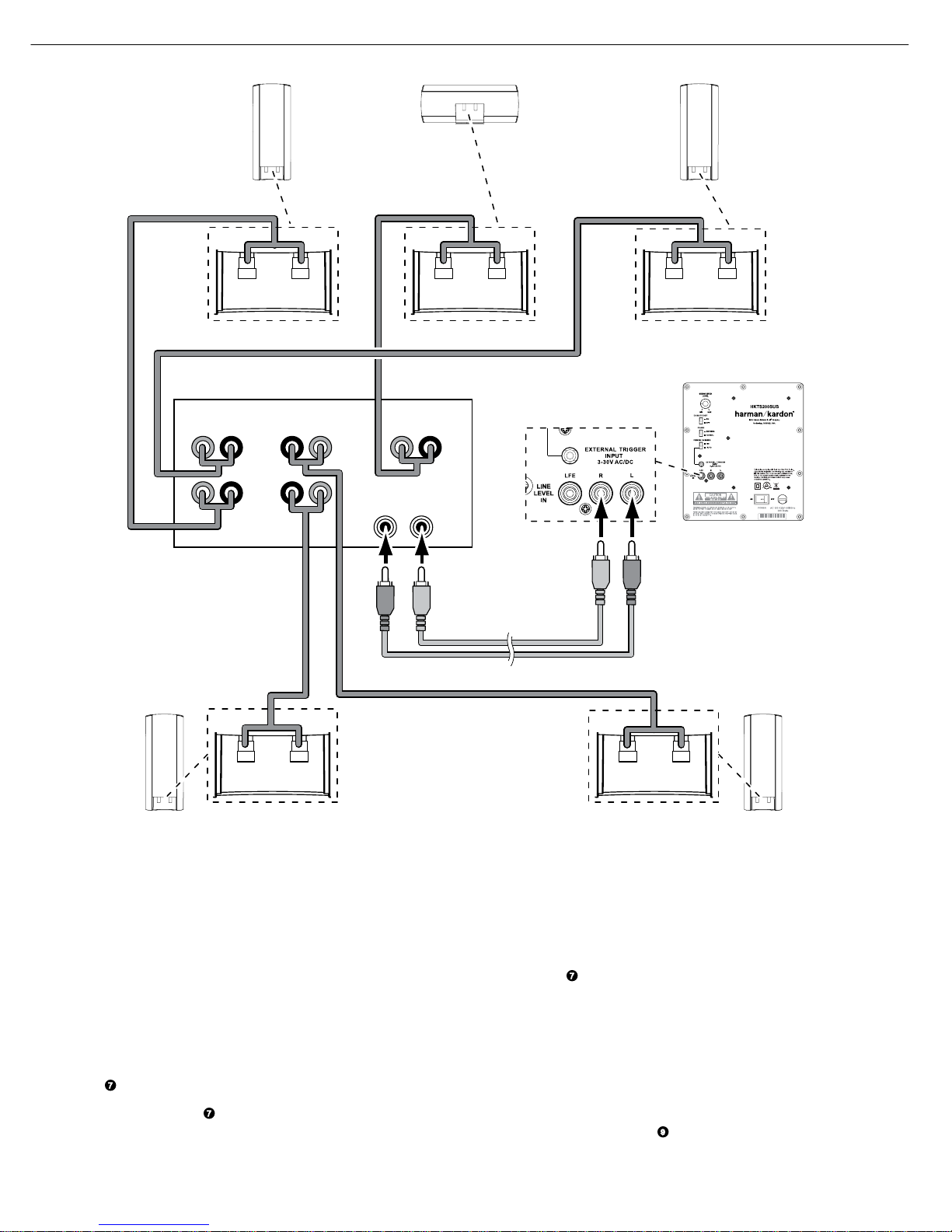
Connecting the Subwoofer to a Receiver
or Preamp/Processor With Line Outputs
Use this installation method for receivers and preamp/processors that
do not have a dedicated subwoofer output, but do have preamp-level
(volume-controlled) line outputs. If the receiver or preamp/processor
has a dedicated subwoofer output with low-pass filtering, see Connect-
ing the Subwoofer to a Receiver or Preamp/Processor With a Dedicated
Subwoofer Output, on page 8.
If you’re connecting to a receiver with left and right line outputs that
are not connected to amplifier inputs, connect the LFE (purple) connector of the supplied combination LFE and trigger cable to one of those
outputs and to either of the HKTS200SUB’s Line-Level L/R In Con-
nectors . Use a second RCA cable ( not supplied) to connect the other
receiver or preamp line output to the other of the HKTS200SUB’s Line-
Level L/R In Connectors .
If you’re connecting to a receiver or preamp /processor with left and
right line outputs that are connected to amplifier front left and right
7
7
inputs, connect the single ends of Y-adapters (not supplied) to
the receiver’s or processor’s left and right line outputs. Connect one
of the Y-adapter’s double ends to the HK TS200SUB’s Line-Level L/R
In Connectors , and connect the other double end to your
amplifier’s front left and right inputs.
Connect each satellite speaker and the center speaker to the
corresponding speaker terminals on your receiver or amplifier.
In your receiver or preamp/processor’s setup menu, configure it for
Subwoofer ON, and set the front left, front right, center, and surround
speakers to Small.
After you have made and verified all connections, plug the
HKTS200SUB’s AC Power Cord into an active AC outlet.
7
9
Page 9
LEFT
LFE SUB
OUTPUT
TRIGGER
OUT
+– +–
+ –
+–
+ –
+–
+ –
RIGHT
SURROUNDFRONT CENTER
PL0004-01001
Subwoofer
Receiver
Trigger Cable
(Black Ends)
HKTS200SUB harman/kardon
8
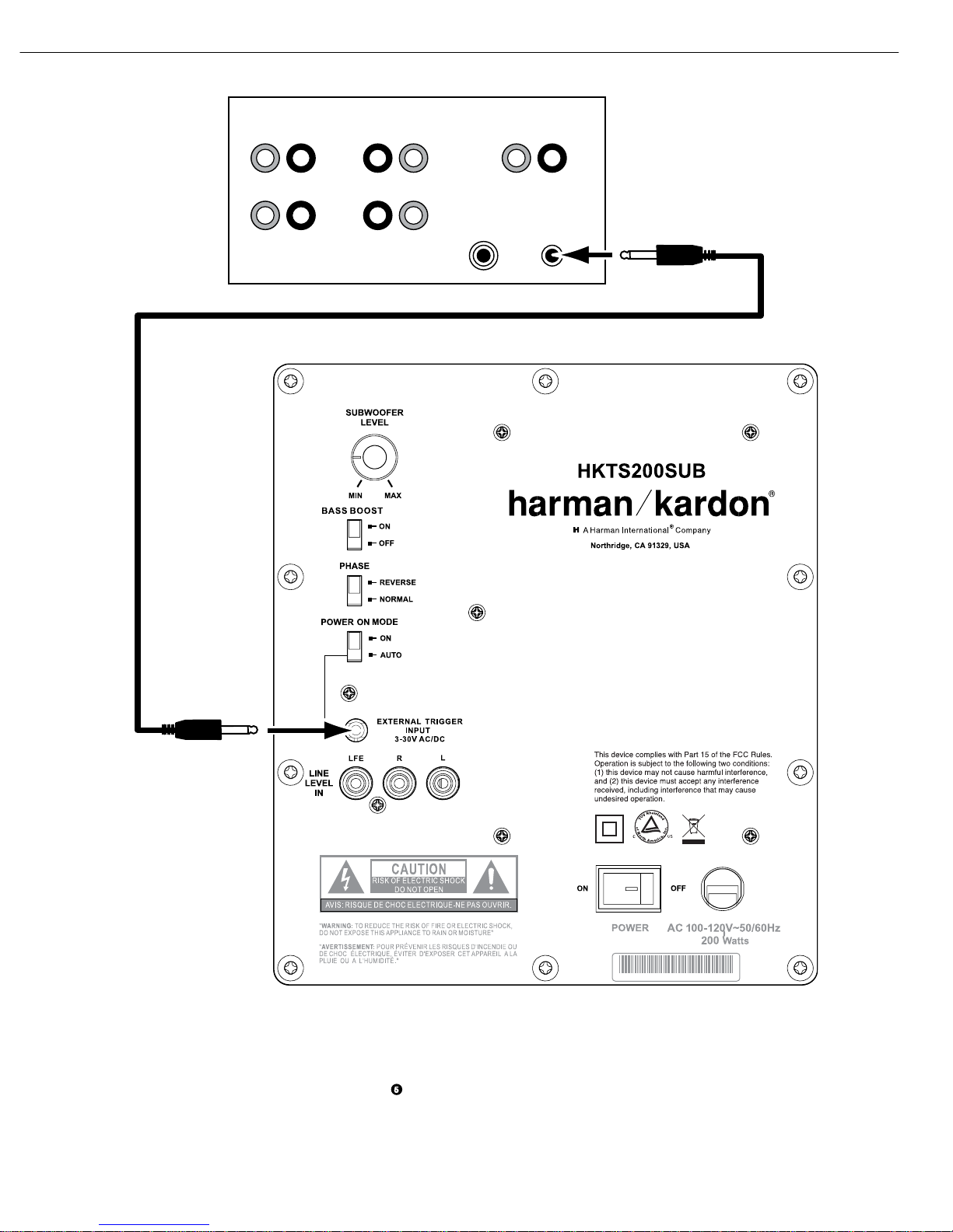
Connecting to a Trigger Voltage Source
If your preamp/processor or another audio/video component has a trigger
voltage connection that supplies between 3 and 30V (AC or DC), connect
it to the HKTS200SUB’s External Trigger Input Connector . If the
component’s trigger voltage connection has a 3.5mm mini jack you can
use the supplied combination LFE/trigger cable to make the connection.
NOTE: Please do not connect the subwoofer ON /OFF trigger cable to the
5
Remote Control Output (IR Out) of your home cinema system or surround
receiver. This could lead to malfunction.
Page 10
HKTS200SUB harman/kardon
9
Operation
Troubleshooting
Turning the Subwoofer On and Off
Set the HKTS200SUB’s Power Switch to the ON position.
• If the Power On Mode Switch is set to AUTO,
the HK TS200SUB will automatically turn itself on when it receives
an audio signal, and it will go into standby mode when it has
received no audio signal for 15 minutes. The HKTS200 SUB’s LED
will illuminate white when the subwoofer is on, and will not be
illuminated when the subwoofer is in standby.
• If the Power On Mode Switch is set to ON, the HK TS20 0SUB
will remain on at all times. The HK TS200 SUB’s LED will illuminate
white.
• If the External Trigger Input Connector is connected to a
trigger voltage source, the HKTS200SUB will turn on whenever a
trigger voltage is present, and will turn off after the trigger voltage
ceases, regardless of the position of the Power On Mode Switch .
If you will be away from home for an extended period of time, or if
you will not be using the subwoofer for an extended period, switch
the Power Switch to the OFF Position.
8
8
4
4
5
4
Subwoofer Adjustments: Volume
Use the Subwoofer Level Control to set the HKTS200SUB’s
volume. Turn the knob clockwise to increase the subwoofer’s volume; turn the knob counterclockwise to decrease the subwoofer’s
volume.
1
Subwoofer Adjustments: Phase
The Phase Switch determines whether the HK TS200SUB’s
piston-like action moves in and out in phase with the satellite
speakers. If the subwoofer were to play out of phase with the satellite speakers, the sound waves produced by the subwoofer could
be canceled out, reducing bass performance and sonic impact.
This phenomenon depends in part on the relative placement of all
the speakers in the room.
Although in most cases the Phase Switch should be left in the
NORMAL position, there is no absolute correct setting for the
Phase Switch . When the HK TS200SUB is properly in phase
with the satellite speakers, the sound will be clearer and have
maximum impact. This will make percussive sounds like drums,
piano and plucked strings sound more lifelike. The best way to
set the Phase Switch is to listen to music that you are familiar
with and set the switch in the position that gives drums and other
percussive sounds maximum impact.
3
3
3
3
Subwoofer Adjustments: Bass Boost
When set to the ON position, the Bass Boost Switch enhances
low-frequency performance, resulting in bass with more impact,
which you may prefer while watching movies or listening to music.
There is no harm in experimenting with this control – set ting the
switch to the OFF position will return normal low-frequency
performance.
2
If there is no sound from any of the speakers :
• Check that the receiver/amplifier is on and a source is playing.
• Make sure that all wires and connections between the receiver/amplifier
and the speakers are connected properly.
• Make sure none of the speaker wires is frayed, cut or punctured.
• Review the proper operation of your receiver/amplifier.
If there is no sound coming from one speaker:
• Check that the balance control on your receiver/amplifier is not set all the
way to one channel.
• Check your receiver /amplifier’s speaker setup procedure to make sur e that
the speaker in question has been enabled and its volume level has not been
turned all the way down.
• Make sure that all wires and connections between the receiver/amplifier
and the speaker are connected properly.
• Make sure the speaker wires are not frayed, cut or punctured.
If there is no sound coming from the center speaker:
• Check your receiver /amplifier’s speaker setup procedure to make sur e that
the center speaker has been enabled and its volume level has not been
turned all the way down.
• Make sure that all wires and connections between the receiver/amplifier
and the center speaker are connected properly.
• Make sure the speaker wires are not frayed, cut or punctured.
• If your receiver is operating in Dolby
center speaker is not set to Phantom.
If there is no sound coming from the surround speakers:
• Check your receiver /amplifier’s speaker setup procedure to make sur e that
the surround speakers have been enabled and their volume levels have not
been turned all the way down.
• Make sure that all wires and connections between the receiver/amplifier
and the surround speakers are connected properly.
• Make sure the speaker wires are not frayed, cut or punctured.
• Review proper operation of your receiver/processor and its surround-
sound features.
• Make sure the movie or TV show you’re watching has been re cor ded in a
surround-sound mode. If it is not, check to see if your receiver/amplifier has
a different surround-sound mode that you can use.
• Review the operation o f your DVD player and the DV D jacket to ma ke sure the
DVD features the desired Dolby Digital or DTS
and that you have properly selected that mode using both the DV D player’s
menu and the disc’s menu.
If there is no sound coming from the subwoofer:
• Check that the subwoofer’s Power Cord is plugged in to a working
AC outlet.
• Check that the subwoofer’s Power Switch is in the ON position.
• Check that the Subwoofer Level Control is not turned all the way down
(fully counterclockwise).
• Check the audio connection between your re ceiver/pr ocessor a nd
the subwoofer.
• Check your receiver /amplifier’s speaker setup procedure to make sur e that
the subwoofer has been enabled and its volume level has not been turned
all the way down.
If the system plays at low volumes but shuts of f as volume is increased:
• Make sure that all wires and connections between the receiver/amplifier
and the speakers are connected properly.
• Make sure none of the speaker wires is frayed, cut or punctured.
• If you’re using m ore than one p air of main speakers, check to be sure tha t
you’re not operating the system below the receiver/amplifier’s minimum
impedance requirements.
®
Pro Logic® mode, make sure that the
®
surround-sound mode,
9
8
1
Page 11
HKTS200SUB harman/kardon
10
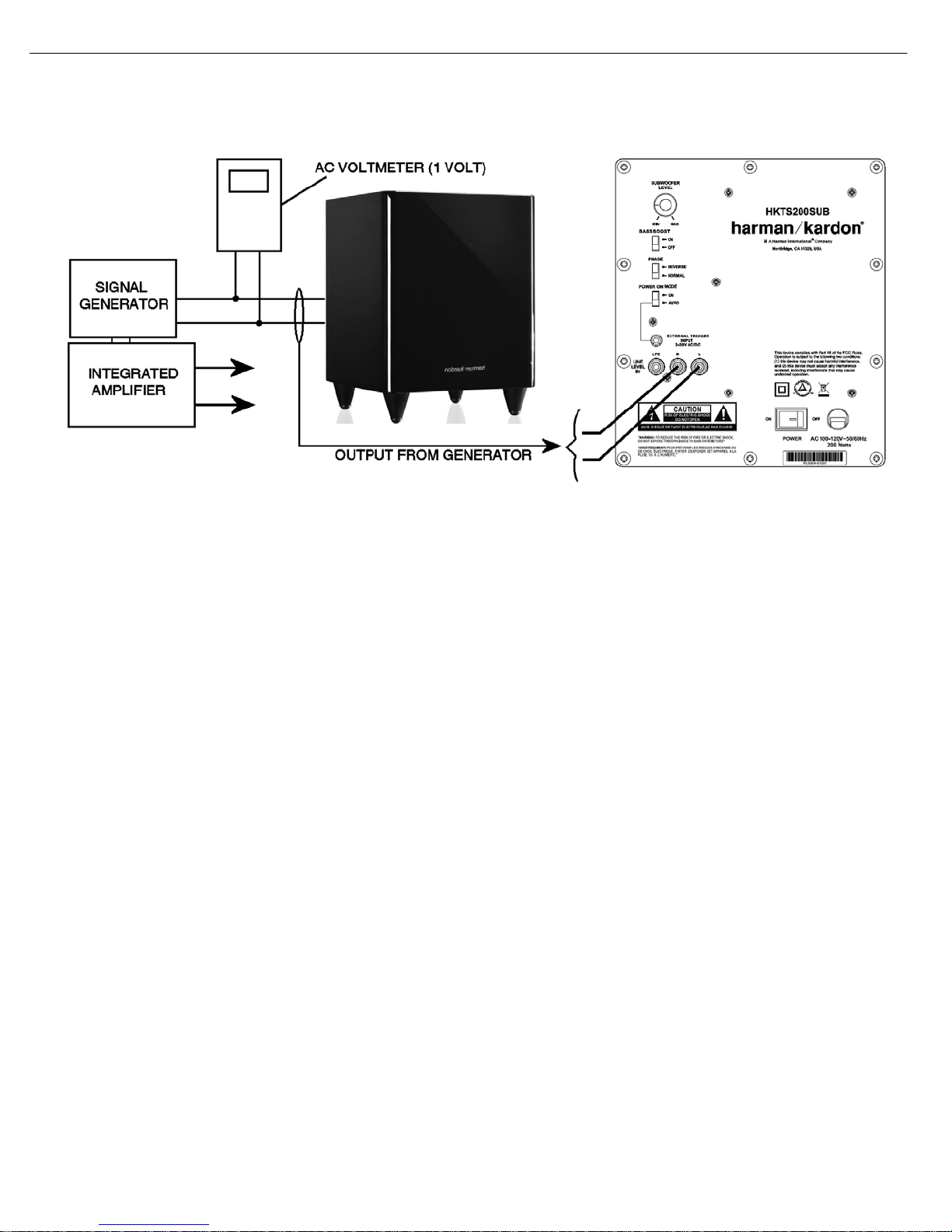
Test Set Up and Procedure
Equipment needed:
• Function/signal generator/sweep generator
• Integrated amplifier
• Multimeter
Initial Control Settings:
• Power Switch OFF; Bass Mode OFF
• Level MIN (Full CCW)
• Phase, Auto/On switches do not matter
General Unit Function (UUT = Unit Under Test)
1) From the signal generator, connect one line level (RCA) cable to the Subwoofer Line Level Input jacks L/R
on the UUT. Use a Y-cable from a mono source if necessary to connect to both inputs. Do not connect to
the single, purple SUB input.
2) Turn on generator; adjust to 100mV, 50 Hz.
3) Plug in UUT; turn the power switch ON. Turn LEVEL control full clockwise (MAX)
4) LED should be white (on top of UUT); immediate and vigorous bass response should be heard and felt
from woofer on bottom of subwoofer.
Sweep Function
1) Follow steps 1-4 above, using a sweep generator as a signal source.
2) Sweep generator from 20Hz to 300Hz. Listen to the cabinet and drivers for any rattles, clicks, buzzes or
any other noises. If any unusual noises are heard, remove woofers and test.
Driver Function
1) Remove woofer from cabinet; detach + and - wire clips.
2) Check DC resistance of woofer; it should be 3.4 ohms ±10%
3) Connect a pair of speaker cables to driver terminals. Cables should be connected to an integrated amplifier
fed by a signal generator. Turn on generator and adjust so that speaker level output is 5.0V.
4) Sweep generator from 20Hz to 1kHz. Listen to driver for any rubbing, buzzing, or other unusual noises.
Page 12
IVAA02071-0001 Wire Tie
MSW108001-0015 -Power Switch
HSP053083-3200-Screw-E*4PCS
GALA00112-0002-AL-Rear Plate
HSP140054-3100-Screw-E*1PC
HSB053083-1120-Screw-E*2PCS
HSP043083-3100-Screw-E*2PCS
DKNA01009-0001-Small knob
IVEA00168-0001-SEAL EVA -OBAE*2PCS
IVEA00168-0002-SEAL EVA -OBAE*2PCS
IVHA12002-0001-SEAL PE PAD-OBAE*2PCS
IVHA12002-0002-SEAL PE PAD-OBAE*2PCS
GCUA00023-0001- BRASS-RCA Shield Cap
DSS100043-0001-Nylon66-SPACER SUPPORT-E*4PCS
APEA00690-4001-PCBA
TPS220200-0408-SMPS
DSS100017-0001-Nylon66-SPACER SUPPORT-E*2PCS
HNT009540-1230-NUT-E*7PCS
BPVA00032-0001-ABS-AMP Rear Cover
GALA00113-0001-AL 5052-Heat sink
XBT090001-M000-BUTYL TAP
HKTS200SUB
harman/kardon
11
Page 13

HKTS200SUB harman/kardon
12
Page 14

MCU
(Renesas R8C/1B Series, 8 kB flash)
(8 MHz)
Audio Processor / PWM
Modulator
(ST309A, 36 bit)
Two 2-pos Slide
Switch’s
I2C
Power Stage
(ST516B, 1x200 W)
Woofer
(4 Ohm)
Analog
Input Buffer (w/
potentiometer for volume
ctrl)
ADC (AK5358A, 24
bit, 32 kHz, 102 dB)
I2S
OSC
(8.192 MHz)
Standby Ctrl
HKTS200SUB Subwoofer Block Diagram
clk
Power Supply
200 W SMPS, 200-264 / 90 –132 V switchable ac input
+48 V for 200 W into 4 Ohms
LED Trigger Input, plug
and level detection
to ADC, for
standby
NTC Temperature
Sensor
ADC
ADC
IO
Power Stage Fault
Detection Circuit
HKTS200SUB
harman/kardon
13
Page 15

CAM Products 2000(TM):
HKTS200SUB
harman/kardon
14
Page 16

CAM Products 2000(TM):
HKTS200SUB
harman/kardon
15
Page 17

CAM Products 2000(TM):
HKTS200SUB
harman/kardon
16
Page 18

HKTS200SUB harman/kardon
17
HKTS200SUB Electrical Parts list
Part number Description Qty Reference Designator
MAIN PCB
Resistors
QCF015030-0000 GP CHIP RES. 0 OHM 1/10W 5% 0603 2 R77 R78
QCF011030-1801 GP CHIP RES. 1.8K OHM 1/10W 1% 0603 1 R3
QCF011030-1002 GP CHIP RES. 10K OHM 1/10W 1% 0603 18
QCF011030-1004 GP CHIP RES. 1M OHM 1/10W 1% 0603 6 R4 R30 R40 R47 R68 R70
QCF015030-5100 GP CHIP RES. 51 OHM 1/10W 5% 0603 6 R7 R15 R16 R18 R31 R32
QCF011030-4991 GP CHIP RES. 4.99K OHM 1/10W 1% 0603 3 R9 R14 R17
QCF011030-4992 GP CHIP RES. 49.9K OHM 1/10W 1% 0603 2 R12 R22
QCF011030-1003 GP CHIP RES. 100K OHM 1/10W 1% 0603 5 R21 R57 R61 R80 R81
QCF011030-2202 GP CHIP RES. 22K OHM 1/10W 1% 0603 4 R25 R23 R24 R82
QCF011030-3301 GP CHIP RES. 3.3K OHM 1/10W 1% 0603 1 R26
QCF011030-1000 GP CHIP RES. 100 OHM 1/10W 1% 0603 2 R33 R60
QCF011030-1001 GP CHIP RES. 1K OHM 1/10W 1% 0603 1 R37
QCF011030-4703 CHIP RES. 470K OHM 1/10W 1% 0603 12
QCF045010-2200 GP CHIP RES. 22 OHM 1/4W 5% 1206 3 R49 R58 R65
QCF011030-2204 GP CHIP RES. 2.2M OHM 1/10W 1% 0603 2 R51 R75
QCF045010-6290 GP CHIP RES. 6.2 OHM 1/4W 5% 1206 2 R52 R67
QCF011030-1333 GP CHIP RES. 133K OHM 1/10W 1% 0603 1 R59
QCF081020-1009 GP CHIP RES. 10 OHM 1/8W 1% 0805 2 R62 R73
QCF011030-1009 GP CHIP RES. 10 OHM 1/10W 1% 0603 1 R71
MVRA02202-1020 CNTL ROTRY 1K OHM LEVEL 1 VR1
R2 R5 R6 R10 R13 R20 R27 R28 R29 R34
R35 R42 R44 R45 R53 R54 R56 R79
R38 R39 R41 R43 R48 R50 R63 R64 R66
R69 R72 R74
Capacitors
C1 C2 C3 C7 C15 C17 C19 C25 C26 C34
PXL456470-1040 GP CHIP CAP 0.1uF 50V 10% 35
PXL410370-1220 GP CHIP CAP 1.2nF 50V 5% 4 C4 C5 C33 C48
PXL410370-2200 GP CHIP CAP 22pF 50V 5% 6 C8 C9 C16 C28 C29 C30
PXL456470-1010 GP CHIP CAP 100pF 50V 10% 9 C11 C21 C22 C24 C37 C43 C99 C100 C6
PYL456420-1060 CHIP CAP 10uF 6.3V 10% 0805 X7R 4 C13 C44 C12 C18
PXL456470-2240 CHIP CAP 220nF 50V 10% 1 C32
PXL456470-4740 GP CHIP CAP 470NF 50V 10% 3 C41 C71 C97
PXL456470-2210 GP CHIP CAP 220pF 50V 10% 1 C42
PYL439520-2260 CHIP CAP 22uF 6.3V 20% 3 C50 C85 C92
PXL4564A0-1040 CHIP CAP 0.1uF 100V 10% 5 C52 C65 C67 C79 C83
PXL456470-1030 GP CHIP CAP 0.01uF 50V 10% 2 C59 C90
PXL4564A0-3310 CHIP CAP 330pF 100V 10% 4 C63 C66 C69 C72
PXL4564A0-1020 CHIP CAP 1nF 100V 10% 3 C64 C68 C78
PXL456440-1050 GP CHIP CAP 1uF 16V 10% 4 C73 C27 C31 C98
PXL456470-1020 GP CHIP CAP 0.001 uF 50V 10% 1 C75
PYL4564A0-4740 GP CHIP CAP 470NF 100V 10% 2 C61 C74
PZL4564A4-1051 GP CHIP CAP 1uF 100V 10% 1206 X7R 3 C62 C70 C80
PZL4564A0-2250 GP CHIP CAP 2.2uF 100V 10% 3 C53 C60 C77
PME099540-2200 GP COND ELECT 22uF 16V 20% 5x11mm 4 C10 C14 C20 C82
PME099540-1010 GP COND ELECT 100uF 16V 20% 5X11 2 C89 C94
PME999540-2200 COND ELECT 22uF 16V 20% 105' 4x7 1 C96
PLE599580-1020 COND ELECT 1000uF 63V 20% 105' 16x25 1 C51
Semiconductors
C36 C38 C39 C40 C45 C46 C47 C49 C54
C55 C56 C57 C58 C76 C81 C84 C86 C87
C88 C91 C93 C95 C23 C101 C102
RCI700405-0002 IC 5P NC7SZ04M5X MA05B TinyLogic UHS Inverter 1 IC1
RCI005343-0001 IC ADC 10 PIN CS5343 CIRRUS Multi-Bit Audio A/D Converter 1 IC2
RCI000720-0001 IC 8P TL072CDR SOIC ST DUAL OP AMP 1 IC3
RCI000309-0001 GP IC 64P STA309A Multi-channel digital audio processor 1 IC4
RCI000809-0008 GP IC 3P AZ809ANSTR-E1 MICRO RESET CIRCUIT 1 IC5
RCI052114-0001 IC 20P R5F211B4DD48S PLSP0020JB-A RENESAS PROCESSOR 1 IC6
Page 19

HKTS200SUB harman/kardon
18
Part number Description Qty Reference Designator
RCI111733-1102
RCI111750-0001 3P LM1117MPX-5.0 SOT-223 Low-Dropout Linear Regulator 1 IC8
RCI000516-0001 IC 36P STA516B SO36 60 V 6 A quad power half bridge 1 IC9
RCP000856-0001 GP TRANSISTOR PNP BC856B SOT-23 2 T3 T8
RCP003906-0002 CHIP TRANSISTOR 3P PNP MMBT3906 PNP SOT23 1 T7
RCN000846-0001 GP TRANSISTOR NPN BC846B SOT23 4 T4 T5 T9 T10
RCN003904-0008 TRANSISTOR NPN MMBT3904 SOT-23 FAIRCHILD 2 T2 T6
RCD100540-0010 GP DIODE CHIP BAT54S (3PIN) 2 D1 D6
RCZ005002-0020 CHIP ZENER 2.7V 5% 0.5W LL34 2 ZD1 ZD2
3P AP1117E33LA SOT223 Low Drop Pos Adjustable/Fixed-Mode Regulator
1 IC7
TPS220200-0407 SMPS power supply (120v) 1
TPS220200-0408 SMPS power supply (230v) 1
Miscellaneous
RNT000030-1002 NTC 10k Ohm 1%,0603, MURATA 1 R36
SCB008051-6010 CHIP BEAD 600 OHM 25% AT 100MHZ SMD 0805 7 B1 B3 B4 B5 B6 B8 B9
JCQA13010-1251 SMD CHIP CRYSTAL 12.288MHz 30ppm 1 X1
CCP254260-0104 HEAD PIN 4P P2.54xH11.5MM 1 CN2
CCN396020-0102 GP CONNECTOR 2 PIN LEOCO 3951 1 SP1
CJRA03401-0010 RCA JACK RCA313 WHITE/RED/PURPLE 1 J1
CJMA35002-3010 PHONE JACK 3.5mm HSJ-035-09-K 1 J2
VWA310054-0002 C/W 2P 100mm 2468#18 RED-BLACK 1 CN1
VWA010034-0001 C/W 4P 90mm 1007#26 BLACK/WHITE/RED 1 CN4
VWA200056-0001 C/W 2P 210mm 2468#26 RED/BLACK 1 LD1
SINA03701-1000 INDUCTOR 10UH 20% D0.9x8.5TS 2 L1 L2
DHU109001-0001 PCB HOUSING L11.5xW8.5xH11.2xT0.8 1 M1
MSWA04001-0010 SLIDE SWITCH SK-22F03 6 PIN BASS/PHASE/AUTO 3 S1 S2 S3
GCUA00023-0001 HKTS30-RCA SHIELD CAP 1 J6
SFB005002-6000 BEAD FERIT 60 OHM 100MHz 3.5x6mm 1 B7
VPAA14013-0010 AC power cord (120v) 1
MSW108001-0015 AC power switch 1
GALA00112-0001 Aluminum amp plate (silkscreened) 1
BPVA00032-0001-ABS-AMP
GALA00113-0001-AL Heatsink 1
DKNA01009-0001 Level knob 1
IVAA02071-0001 Strain Relief Plug 1
Plastic amp cover 1
Page 20

HKTS200SUB
harman/kardon
IC6
IC4
IC3
IC8
19
Page 21

HKTS200SUB
harman/kardon
T2,T6
T7
IC9
IC1
IC5
T4,T5,T9,T10
20
Page 22

HKTS200SUB
harman/kardon
IC2
T3,T8
D1,D6
21
Page 23

REJ09B0252-0110
16
R8C/1A Group, R8C/1B Group
Hardware Manual
RENESAS 16-BIT SINGLE-CHIP MICROCOMPUTER
M16C FAMILY / R8C/Tiny SERIES
Rev.1.10
All information contained in these materials, including products and product specifications,
represents information on the product at the time of publication and is subject to change by
Renesas Technology Corp. without notice. Please review the latest information published
by Renesas Technology Corp. through various means, including the Renesas Technology
Corp. website (http://www.renesas.com).
HKTS200SUB
harman/kardon
22
Page 24

R8C/1A Group, R8C/1B Group 1. Overview
1.5 Pin Assignments
Figure 1.4 shows Pin Assignments for PLSP0020JB-A Package (Top View), Figure 1.5 shows Pin
Assignments for PRDP0020BA-A Package (Top View) and Figure 1.6 shows Pin Assignments for
PWQN0028KA-B Package (Top View).
Figure 1.4 Pin Assignments for PLSP0020JB-A Package (Top View)
1
2
3
4
5
6
7
8
9
10
20 P3_4/SCS/SDA/CMP1_1
19 P3_3/TCIN/INT3/SSI00/CMP1_0
18 P1_0/KI0/AN8/CMP0_0
17
P1_1/KI1/AN9/CMP0_1
16 P4_2/VREF
15 P1_2/KI2/AN10/CMP0_2
14 P1_3/KI3/AN11/TZOUT
13 P1_4/TXD0
12 P1_5/RXD0/CNTR01/INT11
11 P1_6/CLK0/SSI01
P3_5/SSCK/SCL/CMP1_2
P3_7/CNTR0/SSO/TXD1
RESET
XOUT/P4_7
(1)
VSS/AVSS
XIN/P4_6
VCC/AVCC
MODE
P4_5/INT0/RXD1
P1_7/CNTR00/INT10
PIN assignments (top view)
Package: PLSP0020JB-A (20P2F-A)
R8C/1A Group
R8C/1B Group
NOTE:
1. P4_7 is an input-only port.
R8C/1A Group, R8C/1B Group
SINGLE-CHIP 16-BIT CMOS MICROCOMPUTER
1. Overview
These MCUs are fabricated using the high-performance silicon gate CMOS process, embedding the R8C/
Tiny Series CPU core, and is packaged in a 20-pin molded-plastic LSSOP, SDIP or a 28-pin plastic moldedHWQFN. It implements sophisticated instructions for a high level of instruction efficiency. With 1 Mbyte of
address space, they are capable of executing instructions at high speed.
Furthermore, the R8C/1B Group has on-chip data flash ROM (1 KB × 2 blocks).
The difference between the R8C/1A Group and R8C/1B Group is only the presence or absence of data
flash ROM. Their peripheral functions are the same.
1.1 Applications
Electric household appliances, office equipment, housing equipment (sensors, security systems),
general industrial equipment, audio equipment, etc.
REJ09B0252-0110
Rev.1.10
Mar 17, 2006
HKTS200SUB
harman/kardon
23
Page 25

R8C/1A Group, R8C/1B Group 1. Overview
Figure 1.5 Pin Assignments for PRDP0020BA-A Package (Top View)
1
2
3
4
5
6
7
8
9
10
20 P3_4/SCS/SDA/CMP1_1
19 P3_3/TCIN/INT3/SSI00/CMP1_0
18 P1_0/KI0/AN8/CMP0_0
17 P1_1/KI1/AN9/CMP0_1
16 P4_2/VREF
15 P1_2/KI2/AN10/CMP0_2
14 P1_3/KI3/AN11/TZOUT
13 P1_4/TXD0
12 P1_5/RXD0/CNTR01/INT11
11 P1_6/CLK0/SSI01
P3_5/SSCK/SCL/CMP1_2
P3_7/CNTR0/SSO/TXD1
RESET
XOUT/P4_7
(1)
VSS/AVSS
XIN/P4_6
VCC/AVCC
MODE
P4_5/INT0/RXD1
P1_7/CNTR00/INT10
R8C/1A Group
R8C/1B Group
Package: PRDP0020BA-A (20P4B)
NOTE:
1. P4_7 is an input-only port.
PIN assignments (top view)
HKTS200SUB
harman/kardon
24
Page 26

R8C/1A Group, R8C/1B Group 1. Overview
Rev.1.10 Mar 17,
1.6 Pin Functions
Table 1.5 lists Pin Functions, Table 1.6 lists Pin Name Information by Pin Number of PLSP0020JB-A,
PRDP0020BA-A Packages and Table 1.7 lists Pin Name Information by Pin Number of PWQN0028KAB Package.
I: Input O: Output I/O: Input and output
Table 1.5 Pin Functions
Type Symbol I/O Type Description
Power Supply Input VCC, VSS I Apply 2.7 V to 5.5 V to the VCC pin.
Apply 0 V to the VSS pin.
Analog Power
Supply Input
AVCC, AVSS I Power supply for the A/D converter
Connect a capacitor between AVCC and AVSS.
Reset Input RESET
I Input “L” on this pin resets the MCU.
MODE MODE I Connect this pin to VCC via a resistor.
Main Clock Input XIN I These pins are provided for main clock generation
circuit I/O. Connect a ceramic resonator or a
crystal oscillator between the XIN and XOUT pins.
To use an external clock, input it to the XIN pin and
leave the XOUT pin open.
Main Clock Output XOUT O
INT
Interrupt INT0, INT1, INT3 I INT interrupt input pins
Key Input Interrupt KI0
to KI3 I Key input interrupt input pins
Timer X CNTR0 I/O Timer X I/O pin
CNTR0 O Timer X output pin
Timer Z TZOUT O Timer Z output pin
Timer C TCIN I Timer C input pin
CMP0_0 to CMP0_2,
CMP1_0 to CMP1_2
O Timer C output pins
Serial Interface CLK0 I/O Transfer clock I/O pin
RXD0, RXD1 I Serial data input pins
TXD0, TXD1 O Serial data output pins
Clock synchronous
serial I/O with chip
select (SSU)
SSI00, SSI01 I/O Data I/O pin.
SCS
I/O Chip-select signal I/O pin
SSCK I/O Clock I/O pin
SSO I/O Data I/O pin
I2C bus Interface
SCL I/O Clock I/O pin
SDA I/O Data I/O pin
Reference Voltage
Input
VREF I Reference voltage input pin to A/D converter
A/D Converter AN8 to AN11 I Analog input pins to A/D converter
I/O Port P1_0 to P1_7,
P3_3 to P3_5, P3_7,
P4_5
I/O CMOS I/O ports. Each port has an I/O select
direction register, allowing each pin in the port to
be directed for input or output individually.
Any port set to input can be set to use a pull-up
resistor or not by a program.
P1_0 to P1_3 also function as LED drive ports.
Input Port P4_2, P4_6, P4_7 I Input-only ports
HKTS200SUB
harman/kardon
25
Page 27

R8C/1A Group, R8C/1B Group 1. Overview
Rev.1.10 Mar 1
Table 1.6 Pin Name Information by Pin Number of PLSP0020JB-A, PRDP0020BA-A Packages
Pin
Number
Control
Pin
Port
I/O Pin Functions for Peripheral Modules
Interrupt Timer
Serial
Interface
Clock
Synchronous
Serial I/O with
Chip Select
I
2
C bus
Interface
A/D
Converter
1 P3_5 CMP1_2 SSCK SCL
2P3_7
CNTR0
TXD1 SSO
3
RESET
4XOUTP4_7
5 VSS/AVSS
6XINP4_6
7VCC/AVCC
8MODE
9P4_5
INT0
RXD1
10 P1_7
INT10
CNTR00
11 P1_6 CLK0 SSI01
12 P1_5
INT11
CNTR01 RXD0
13 P1_4 TXD0
14 P1_3
KI3
TZOUT AN11
15 P1_2
KI2
CMP0_2 AN10
16 VREF P4_2
17 P1_1
KI1
CMP0_1 AN9
18 P1_0
KI0
CMP0_0 AN8
19 P3_3
INT3
TCIN/
CMP1_0
SSI00
20 P3_4 CMP1_1
SCS
SDA
HKTS200SUB
harman/kardon
26
Page 28

R8C/1A Group, R8C/1B Group 1. Overview
Rev.1.10 Mar 1
Table 1.7 Pin Name Information by Pin Number of PWQN0028KA-B Package
Pin
Number
Control
Pin
Port
I/O Pin Functions for Peripheral Modules
Interrupt Timer
Serial
Interface
Clock
Synchronous
Serial I/O with
Chip Select
I
2
C bus
Interface
A/D
Converter
1NC
2XOUTP4_7
3 VSS/AVSS
4NC
5NC
6XINP4_6
7NC
8VCC/AVCC
9MODE
10 P4_5
INT0
RXD1
11 P1_ 7
INT10
CNTR00
12 P1_6 CLK0 SSI01
13 P1_5
INT11
CNTR01 RXD0
14 P1_4 TXD0
15 NC
16 P1_3
KI3
TZOUT AN11
17 P1_2
KI2
CMP0_2 AN10
18 NC
19 NC
20 VREF P4_2
21 NC
22 P1_1
KI1
CMP0_1 AN9
23 P1_0
KI0
CMP0_0 AN8
24 P3_3
INT3
TCIN/CMP1_0 SSI00
25 P3_4 CMP1_1
SCS
SDA
26 P3_5 CMP1_2 SSCK SCL
27 P3_7
CNTR0
TXD1 SSO
28
RESET
HKTS200SUB
harman/kardon
27
Page 29

http://www.cirrus.com
Advance Product Information
This document contains information for a new product.
Cirrus Logic reserves the right to modify this product without notice.
98 dB, 96 kHz, Multi-Bit Audio A/D Converter
Features
! Advanced Multi-Bit ∆Σ Architecture
! 24-bit Conversion
! Supports Audio Sample Rates Up to 108 kHz
! 98 dB Dynamic Range at 5 V
! -90 dB THD+N
! Low-Latency Digital Filter
! High-Pass Filter to Remove DC Offsets
! Single +3.3 V or +5 V Power Supply
! Power Consumption Less Than 50 mW
! Master or Slave Operation
! Slave Mode Speed Auto-Detect
! Master Mode Default Settings
! 256x or 384x MCLK/LRCK Ratio
! CS5343 Supports I²S Audio Format
! CS5344 Supports Left-Justified Audio Format
General Description
The CS5343/4 is a complete analog-to-digital converter
for digital audio systems. It performs sampling, analogto-digital conversion, and anti-alias filtering, generating
24-bit values for both left and right inputs in serial form
at sample rates up to 108 kHz per channel.
The CS5343/4 uses a 3rd-order, multi-bit Delta-Sigma
modulator followed by a digital filter, which removes the
need for an external anti-alias filter.
The CS5343/4 also features a high-impedance sampling network which eliminates costly external
components such as op-amps.
The CS5343/4 is available in a 10-pin TSSOP package
for both Commercial (-10° to +70° C) and Automotive
grades (-40° to +85° C). The CDB5343 Customer Demonstration Board is also available for device evaluation
and implementation suggestions. Please refer to the
“Ordering Information” on page 21 for complete details.
The CS5343/4 is ideal for audio systems requiring wide
dynamic range, negligible distortion and low noise, such
as set-top boxes, DVD-karaoke players, DVD recorders, A/V receivers, and automotive applications.
High-Pass
Filter
High-Pass
Filter
Low-Latency
Digital Filters
VA
3.3 V to 5 V
Internal
Reference
Voltages
High-Z
Sampling
Network
Auto-detect
MCLK Divider
Master
Clock
Single-Ended
Analog Input
Low-Latency
Digital Filters
High-Z
Sampling
Network
Single-Ended
Analog Input
SCLK
LRCK
SDOUT
FILT+
VQ
AINR
AINL
Serial Port
Slave Mode
Auto-detect
High-Pass
Filter
AUGUST '06
DS687A4
CS5343/4
HKTS200SUB harman/kardon
28
Page 30

CS5343/4
1. PIN DESCRIPTIONS
Pin Name Pin # Pin Description
SDOUT 1
Serial Audio Data Output (Output) - Output for two’s complement serial audio data. Also selects Master
or Slave Mode.
SCLK 2 Serial Clock (Input/Output) - Serial clock for the serial audio interface.
LRCK 3
Left Right Clock (Input/Output) - Determines which channel, Left or Right, is currently active on the
serial audio data line.
MCLK 4 Master Clock (Input) - Clock source for the delta-sigma modulator and digital filters.
FILT+ 5 Positive Voltage Reference (Output) - Positive reference voltage for the internal sampling circuits.
AINL
AINR
68Analog Input (Input) - The full-scale analog input level is specified in the Analog Characteristics specifi-
cation table.
VQ 7 Quiescent Voltage (Output) - Filter connection for the internal quiescent reference voltage.
GND 9 Ground (Input) - Ground reference. Must be connected to analog ground.
VA 10 Power (Input) - Positive power supply for the digital and analog sections.
1
2
3
4
5
6
7
8
9
10
SDOUT
SCLK
LRCK
MCLK
FILT+
VA
GND
AINR
VQ
AINL
HKTS200SUB harman/kardon
29
Page 31

HKTS200SUB harman/kardon
30
NC7SZ04 TinyLogic
October 1996
Revised June 2000
NC7SZ04
TinyLogic
General Description
The NC7SZ04 is a single inverter from Fairchild’s Ultra
High Speed Series of TinyLogic
with advanced CMOS technology to achieve ultra high
speed with high output drive while maintaining low static
power dissipation o ver a very broad V
The device is speci fied to operate over the 1.8V to 5.5V
range. The inputs and output are high impedance
V
CC
when V
dent of V
is 0V. Inputs tolerate voltages up to 6V indepen-
CC
operating voltage.
CC
UHS Inverter
. The device is fab ricat ed
operating range.
CC
Features
■ Space saving SOT23 or SC70 5-lead package
■ Ultra High Speed; t
■ High Output Drive; ±24 mA at 3V V
■ Broad VCC Operating Range; 1.8V to 5.5V
■ Matches the performance of LCX when operated at
3.3V V
CC
■ Power down high impedance inputs/output
■ Overvoltage tolerant inputs facilitate 5V to 3V
translation
■ Patented noise/EMI reduction circuitry implemented
2.4 ns typ into 50 pF at 5V V
PD
CC
CC
Ordering Code:
Order Package Product Code
Number Number Top Mark
NC7SZ04M5 MA05B 7Z04 5-Lead SOT23, JEDEC MO-178, 1.6mm 250 Units on Tape and Reel
NC7SZ04M5X MA05B 7Z04 5-Lead SOT23, JEDEC MO-178, 1.6mm 3k Units on Tape and Reel
NC7SZ04P5 MAA05A Z04 5-Lead SC70, EIAJ SC-88a, 1.25mm Wide 250 Units on Tape and Reel
NC7SZ04P5X MAA05A Z04 5-Lead SC70, EIAJ SC-88a, 1.25mm Wide 3k Units on Tape and Reel
Package Description Supp lie d As
UHS Inverter
Logic Symbol
IEEE/IEC
Connection Diagram
Pin Descriptions Function Table
Pin Names Description
A Input
Y Output
NC No Connect
H = HIGH Logic Lev el
L = LOW Logic L ev el
TinyLogic is a trademark of Fairchild Semiconductor Corporation.
Input Output
AY
LH
HL
(Top View)
Y = A
Page 32

September 2007 Rev 1 1/67
67
STA309A
Multi-channel digital audio processor with DDX®
Features
! 8 channels of 24-bit DDX
®
! >100 dB SNR and dynamic range
! Selectable 32 kHz - 192 kHz input sample rates
! 6 channels of DSD/SACD input
! Digital gain/attenuation +58 dB to -100 dB in
0.5 dB steps
! Soft volume update
! Individual channel and master gain/attenuation
plus channel trim (-10 dB to +10 dB)
! Up to 10 independent 32-bit user
programmable biquads (EQ) per channel
! Bass/treble tone control
! Pre and post EQ full 8-channel input mix on all
8 channels
! Dual independent limiters/compressors
! Dynamic range compression or anti-clipping
modes
! AutoModes:
– 5-band graphic EQ
– 32 preset EQ curves (rock, jazz, pop, etc.)
– Automatic volume controlled loudness
– 5.1 to 2-channel downmix
– Simultaneous 5.1- and 2-channel downmix
outputs
– 3 preset volume curves
– 2 preset anti-clipping modes
– Preset movie nighttime listening mode
– Preset TV channel/commercial AGC mode
– 5.1, 2.1 bass management configurations
– AM frequency automatic output PWM
frequency shifting
– 8 preset crossover filters
! Individual channel and master soft/hard mute
! Automatic zero-detect and invalid input mute
! Automatic invalid input detect mute
! Advanced PopFree operation
! Advanced AM interference frequency
switching and noise suppression modes
! I
2
S output channel mapping function
! Independent channel volume and DSP bypass
! Channel mapping of any input to any
processing/DDX
®
channel
! DC blocking selectable high-pass filter
! Selectable per-channel DDX
®
damped ternary
or binary PWM output
! Max power correction for lower full-power THD
! Variable per channel DDX
®
o
utput delay control
! 192 kHz internal processing sample rate, 24-bit
to 36-bit precision
Description
The STA309A is a single chip solution for digital
audio processing and control in multi-channel
applications. It provides output capabilities for
DDX
®
(direct digital amplification). In conjunction
with a DDX
®
power device, it provides highquality, high-efficiency, all digital amplification.
The device is extremely versatile, allowing for
input of most digital formats including 6.1/7.1channel and 192 kHz, 24-bit DVD-audio,
DSD/SACD. In 5.1 application the additional 2
channels can be used for audio line-out or
headphone drive. In speaker mode, with 8
channel outputs in parallel, the STA309A can
deliver more than 1 W.
Table 1. Device summary
Order code Package
STA309A TQFP64
TQFP64
HKTS200SUB harman/kardon
31
Page 33

STA309A Block diagram
9/67
1 Block diagram
Figure 1. Block diagram
Figure 2. Channel signal flow
OUT1A/B
OUT2A/B
OUT3A/B
OUT4A/B
OUT5A/B
OUT6A/B
OUT7A/B
OUT8A/B
LRCKI
BICKI
SDI12
SDI34
SDI56
SDI78
SA
SERIAL
DATA
IN
I2C
CHANNEL
MAPPING
VARIABLE
OVER-
SAMPLING
TREBLE,
BASS, EQ
(
BIQUADS
)
VOLUME
LIMITING
SDO78
SDO12
SDO34
SDO56
OVERSAMPLING
VARIABLE
DOWN-
SAMPLING
POWER
DOWN
PWDN
EAPD
PLL
PLLB
XTI
CKOUT
SCL
SDA
LRCKO
BICKO
MVO
SERIAL
DATA
OUT
SYSTEM
CONTROL
SYSTEM TIMING
DDX
1x,2x,4x
Interp
Biq ua ds
B/ T
Vol ume
Limiter
2x
Interp
Distortion
Compensation
NS C_Con PWM
DDX
Output
Interp_Rate
8 Inputs
From I2S
DSD
Conversion
6 Inputs
From DSD
Mapping/
Mix #1
DSDE
Mix #2
PreScale
High - Pa s s
Filte r
Biqu a d#2Biquad#3Biquad#4Biqu a d#5Biquad#6Biquad#7Biquad
#8
Bas s
Hard Set to
-18dB when
AutoMode EQ
(AMEQ)
Hard Set Coeffecients when AutoMode EQ
(AMEQ)
Hard Set
Coeffec ients when
Aut oM od e
Bass Management
Cross over
(AMBMXE)
Hard Set
Coeffec ients when
DeEmphasis
Enable d
(DEMP)
From
Mix#1
Engine
Or
Previous
Channel
Biqu a d # 1 0
Output
(CxBLP)
To
Mix#2
Engine
Treble
User Progammable
Biquad #1 when
High-Pass Bypassed
(HPB)
User Prog rammable
Biquads #9 and #10
When Tone Bypass ed
(CxTCB)
HKTS200SUB harman/kardon
32
Page 34

Pin connections STA309A
10/67
2 Pin connections
Figure 3. Pin connection (top view)
Table 2. Pin description
Pin Type Name Description
1 5-V tolerant TTL input buffer MVO/DSD_CLK
Master volume override/
DSD input clock
6 5-V tolerant TTL input buffer SDI_78/DSD_6
Input serial data channels 7 & 8/
DSD input channel 6
7 5-V tolerant TTL input buffer SDI_56/DSD_5
Input serial data channels 5 & 6/
DSD input channel 5
8 5-V tolerant TTL input buffer SDI_34/DSD_4
Input serial data channels 3 & 4/
DSD input channel 4
9 5-V tolerant TTL input buffer SDI_12/DSD_3
Input serial data channels 1 & 2/
DSD input channel 3
10 5-V tolerant TTL input buffer LRCKI/DSD_2
Input left/right clock/
DSD input channel 2
11 5-V tolerant TTL input buffer BICKI/DSD_1
Input serial clock/
DSD input channel 1
15
5-V tolerant TTL schmitt
trigger input buffer
RESET Global reset
16
CMOS input buffer with
pull-down
PLL_BYPASS Bypass phase locked loop
1
2
3
5
6
4
7
8
9
10
271128 29 30 31 32
59 58 57 565455 53 52 51 50 49
43
42
41
39
38
40
48
47
46
44
45
SDI_78
NC
GND
GND
MVO
VDD
BICKI
LRCKI
SDI_12
SDI_56
SDI_34
NC
GNDA
VDDA
CKOUT
GND
NC
VDD
OUT8_B
OUT8_A
OUT7_B
OUT7_A
VDD
SDO_34
SDO_12
LRCKONCBICKO
GND
VDD
EAPD
OUT1_A
OUT1_B
OUT3_A
OUT3_B
OUT4_A
OUT5_A
OUT5_B
OUT4_B
OUT2_A
OUT2_B
NC
VDD
GND
STA308APINCON
22 23 24 25 26
60
GND61NC62SDO_56
63
SDO_78
64
PWDN
SA
SDA
SCL
XTI
FILTER_PLL
17 18 19 20 21
37
36
34
33
35
NC
GND
OUT6_A
OUT6_B
VDD
12
13
14
15
16
PLLB
RESET
NC
VDD
GND
HKTS200SUB harman/kardon
33
Page 35

STA309A Pin connections
11/67
17
CMOS input buffer with
pull-down
SA Select address (I
2
C)
18
Bidirectional buffer: 5-V
tolerant TTL schmitt trigger
input; 3.3-V capable 2mA
slew-rate controlled output.
SDA Serial data (I
2
C)
19
5-V tolerant TTL schmitt
trigger input buffer
SCL Serial clock (I
2
C)
20
5-V tolerant TTL schmitt
trigger input buffer
XTI Crystal oscillator input (clock input)
21 Analog pad FILTER_PLL PLL filter
23 Analog ground GNDA PLL ground
24 3.3V analog supply voltage VDDA PLL supply
25
3.3-V capable TTL tristate
4mA output buffer
CKOUT Clock output
29
3.3-V capable TTL 16mA
output buffer
OUT8B PWM channel 8 output B
30
3.3-V capable TTL 16mA
output buffer
OUT8A PWM channel 8 output A
31
3.3-V capable TTL 16mA
output buffer
OUT7B PWM channel 7 output B
32
3.3-V capable TTL 16mA
output buffer
OUT7A PWM channel 7 output A
33
3.3-V capable TTL 16mA
output buffer
OUT6B PWM channel 6 output B
34
3.3-V capable TTL 16mA
output buffer
OUT6A PWM channel 6 output A
38
3.3-V capable TTL 16mA
output buffer
OUT5B PWM channel 5 output B
39
3.3-V capable TTL 16mA
output buffer
OUT5A PWM channel 5 output A
40
3.3-V capable TTL 16mA
output buffer
OUT4B PWM channel 4 output B
41
3.3-V capable TTL 16mA
output buffer
OUT4A PWM channel 4 output A
42
3.3-V capable TTL 16mA
output buffer
OUT3B PWM channel 3 output B
43
3.3-V capable TTL 16mA
output buffer
OUT3A PWM channel 3 output A
47
3.3-V capable TTL 16mA
output buffer
OUT2B PWM channel 2 output B
Table 2. Pin description (continued)
Pin Type Name Description
HKTS200SUB harman/kardon
34
Page 36

Pin connections STA309A
12/67
48
3.3-V capable TTL 16mA
output buffer
OUT2A PWM channel 2 output A
49
3.3-V capable TTL 16mA
output buffer
OUT1B PWM channel 1 output B
50
3.3-V capable TTL 16mA
output buffer
OUT1A PWM channel 1 output A
51
3.3-V capable TTL 4mA
output buffer
EAPD Ext. amp power-down
55
3.3-V capable TTL 2mA
output buffer
BICKO Output serial clock
56
3.3-V capable TTL 2mA
output buffer
LRCKO Output left/right clock
57
3.3-V capable TTL 2mA
output buffer
SDO_12 Output serial data channels 1&2
58
3.3-V capable TTL 2mA
output buffer
SDO_34 Output serial data channels 3&4
62
3.3-V capable TTL 2mA
output buffer
SDO_56 Output serial data channels 5&6
63
3.3-V capable TTL 2mA
output buffer
SDO_78 Output serial data channels 7&8
64
5-V tolerant TTL schmitt
trigger input buffer
PWDN Device power-down
3,12,28,35,
44,52,59
3.3-V digital supply voltage VDD 3.3-V supply
2,4,13,27,
36,45,53,60
Digital ground GND Ground
5, 14, 22,
26,37,46,54,
61
NC Not connected
Table 2. Pin description (continued)
Pin Type Name Description
HKTS200SUB harman/kardon
35
Page 37

HKTS200SUB harman/kardon
36
Page 38

1 2 3 4 5 6
A
B
C
D
654321
D
C
B
A
CX2
C12
C15
C16
C17
R33
R6
1413
4
2
R3
R4
3
R2
C4
R11
R12
15
16
C2
D3
RN
C5
R18
D18
12
R1
C1
7 9 10
R8
LF2
R42
LF1
CX1
F1
RT1
R31R40
R35
T7
R34
C13
R36
R38
T6
R37
C14
R39
DW1
T4 T5
D9
D8
C9
D6
GND
R15
R17
R13R14
GND GND
11
8
6
5
GND
C3
GND
GND
IC1
1
GND
L N
A.2
TR1
D19
CY1
GND
R20
DD1
GND
R30 C11
L1
C10
C8
R28
R7
GND
IC1
DW2
R44
C65
C33
D21
DW3
V+
V+
C6
D1
D22C7GND
123
CN1
D17D13
D16
D14
D10
D12
D11
D15
D20
R9
C19
R5 R10
D7
CY2
GND
HYS3B210-CS
CN2
4
5
219
8
10
6
4
3
11
10
9
10
7
6
!
!
! !
TR2
!
!
!
!
!
!
D23
D2
C32C31
1
2
CN4
NTC
!
C30
C29
C20
IC2
GND
Vref
Vref
C27
C18
GND
R16
9
GND
T8
D25
C26
R47
R26R27
R19
D24
R23
R22 C24
C23
C22
R21
46 8
5
1
32
7
R45
D4
D5
R24
R25
DW6
C21
HV
HV
L2
L3
Q2
R57
R56
C28
GND
R54
R51
Q1
R49
1
2
3
4
CN3
R52
R53
GND
R48
C34
8
R43
IC3
V+
GND
+7V
GND
-7V
STB
!
!
!
HV
CY3
GND
!
R29
TR3
5
!
5
4
2
1
NOTE the SMPS power supply
should be replaced in its entirety
and the schematic is supplied only
for reference
120v part# TPS220200-0407
230v part# TPS220200-0408
HKTS200SUB harman/kardon
37
Page 39

1
1
2
2
3
3
4
4
5
5
6
6
7
7
8
8
D D
C C
B B
A A
1
1
HKTS200SUB
1.1
2009-7-23
E:\Work\HKTS\SCH2.SchDoc
Title
Size:
Date:
File:
Revision:
Sheet
of
A3
Ruben Millyard
Meican.wu
DrawnBy:
ApprovedBy:
P3_5
1
P3_7
2
RESET
3
XOUT
4
VSS
5
XIN
6
VCC
7
MODE
8
P4_5
9
P1_710P1_6
11
P1_5
12
P1_4
13
P1_3
14
P1_2
15
VREF
16
P1_1
17
P1_0
18
P3_3
19
P3_4
20
IC6
R5F211A4
MVO
1
GND
2
VDD3
3
GND
4
NC
5
SDI78
6
SDI56
7
SDI34
8
SDI12
9
LRCKI
10
BICKI
11
VDD3
12
GND
13
NC
14
RESET
15
PLLB
16
SA17SDA18SCL19XTI20PLLF21NC22GND_PL23VDD_PL24CKOUT25NC26GND27VDD328OUT8B29OUT8A30OUT7B31OUT7A
32
OUT6B
33
OUT6A
34
VDD3
35
GND
36
NC
37
OUT5B
38
OUT5A
39
OUT4B
40
OUT4A
41
OUT3B
42
OUT3A
43
VDD3
44
GND
45
NC
46
OUT2B
47
OUT2A
48
OUT1B
49
OUT1A
50
EAPD
51
VDD3
52
GND
53
NC
54
BICKO
55
LRCKO
56
SDO_1257SDO_34
58
VDD59GND
60
NC
61
SDO_5662SDO_78
63
PWDN
64
IC4
STA309A
GND_SUB
1
OUT2B
2
OUT2B
3
VCC2B
4
GND2B
5
GND2A
6
VCC2A
7
OUT2A
8
OUT2A
9
OUT1B
10
OUT1B
11
VCC1B
12
GND1B
13
GND1A
14
VCC1A
15
OUT1A
16
OUT1A
17
NC
18
GND_CLR
19
GND_REG
20
VDD
21
VDD
22
VL
23
CONFIG
24
PWDN
25
TRI_STATE
26
FAULT
27
TH_WAR
28
IN1A
29
IN1B
30
IN2A
31
IN2B
32
VSS
33
VSS
34
VCCSIGN
35
VCCSIGN
36
IC9
STA516B
1
23
IC5
AZ809NSTR
100nF
C38
100nF
C39
+3.3V
100nF
C1
100nF
C2
EAPD
100nF
C15
100nF
C36
+3.3V
+3.3V
100nF
C19
+3.3V
100nF
C17
100nF
C40
+3.3V
3k3
R26
220pF
C42
100pF
C43
1.2nF
C48
100nF
C49
100nF
C46
+3.3V
100nF
C54
100nF
C56
IN5B
EAPD
100nF
C84
B8
+3.3V
100nF
C81
100nF
C76
1000uF
+
C51
2.2uF
C60
0.47uF
C61
2.2uF
C77
0.47uF
C74
22uH
L1
22
R49
330pF
C66
6.2
R67
100nF
C79
100nF
C83
NTC
R36
3.3k
R37
+3.3V
CN2
1nF
C68
100nF
C47
10k
R34
10k
R35
10k
R53
10k
R56
B4
B6
10uF
+
C13
1
23
4
IC7
LM1117-3.3
1nF
C78
SP1
100nF
C52
CN1
RESET
MODE
22uH
L2
*
D4
*
D5
*
D2
*
D3
VCC
VCC
1uF
100V
C70
6.2
R52
100nF
C65
100nF
C67
1nF
C64
VCC
IN5B
IN5A
IN5A
1
2
34
5
NC
GND
VCC
IC1
NC7SZ04
8.192MHz
X1
51
R15
51
R16
51
R18
1.8k
R3
1M
R4
22pF
C8
100nF
C3
100nF
C34
100nF
C25
B1K
1 2
3
VR1
2.7k
R9
49.9k
R12
100pF
C22
10k
R5
51
R31
51
R32
100kR21
220nF
C32
2.7V
ZD1
CN4
100nF
C88
100uF
+
C89
22
R65
1
23
4
IC8
LM1117-5.0
100nF
C93
100uF
+
C94
10
R71
100nF
C91
22uF
+
C92
100nF
C86
22uF
+
C85
10k
R13
100pF
C24
10k
R27
10k
R28
+3.3V
100nF
C87
100nF
C95
+7V
+3.3V
+5V
LD1
LED
10k
R29
Vdd
100
R33
22k
R25
+3.3V
1
2
3
4
5
J2
22K
R23
22K
R24
2.7V
ZD2
470k
R38
1M
R40
BC846B
T4
10nF
C59
470k
R41
1M
R47
470k
R43
470k
R39
VCC
470nF
C71
470k
R50
1M
R55
470k
R48
VCC
BC846B
T5
2.2M
R51
1uF
C73
133k
R59
470k
R63
1M
R68
BC846B
T9
10nF
C90
470k
R66
1M
R70
470k
R69
470k
R64
VCC
470nF
C97
470k
R74
1M
R76
470k
R72
VCC
BC846B
T10
2.2M
R75
SPK+
SPK-
DCP
DCP
1.2nF
C5
22pF
C9
4.99k
R14
10k
R20
49.9k
R22
22
R58
330pF
C69
1uF
100V
C80
1uF
100V
C62
s1
+7V
-7V
1
2
3
4
5
6
7
8
IC3
2
3
1
4
5
J1
s2 s3
2N3904
T2
PHASE
Filter AUTO/ON
L
R
LFE
TRIGGER/AUDIO IN
+48V
2N3906
T7
2N3904
T6
10k
R54
+7V
1nF
C75
100k
R57
100k
R61
10uF
+
C44
+3.3V
22pF
C28
22pF
C29
22pF
C30
22pF
C16
51
R7
2.7V
ZD3
B1
+3.3V
22uF
+
C20
22uF
+
C35
1.2nF
C4
1.2nFC33
4.99k
R17
B7
B5
+3.3V
10
R73
-7V
B9
100
R60
1M
R30
+3.3V
BAT54S
D1
470nF
C41
2N3904
T1
10k
R2
100pF
C6
1.8k
R1
2.2uF
C53
330pF
C63
330pF
C72
100nF
C45
10k
R42
10k
R45
10k
R44
10
R62
22uF16V
+
C82
100nF
C7
100nF
C26
+3.3V
100nF
C58
100nF
C57
100nF
C55
DCP
+3.3V
+5V
-7V
+7V
PDN_ctr
SDA
SCL
IN5A
IN5B
VCC
SPK+
SPK-
EAPD
OUT2
OUT1
308_SDA
308_SCL
M1
PCB_HOLDER
DCP
PDN
AUTO/ON
Vdd
B3
+5V
100pF
C37
22uF
+
C50
PHASE
POWER ON
Temp.Detect
SIGNAL SENSE
LED
TRIGGER
OSC_CTR
100uF16V
+
C96
10k
R10
22uF
+
C14
100pF
C21
10k
R622uF
+
C10
100pF
C11
BC856B
T3
BC856B
T8
0
R77
SPK-
0
R78
SPK+
SDOUT
1
SCLK
2
LRCK
3
FILT+5AINL
6
VQ
7
AINR
8
GND
9
VA
10
MCLK
4
IC2
CS5343
SDTO
SCLK
LRCK
1uF
C98
100nF
C23
1uF
C31
1uF
C27
10k
R79
100k
R80
100k
R81
100pF
C99
100pF
C100
10uF
C12
10uF
C18
MCLK
CN3
+3.3V
FILTER
100nF
C101
crossover
(DNP)
(DNP)
(DNP)
(DNP)
100nF
C102
BAT54S
D6
22K
R82
JACK SENSE
(DNP)
(DNP)
HKTS200SUB
harman/kardon
38
 Loading...