

Page 1
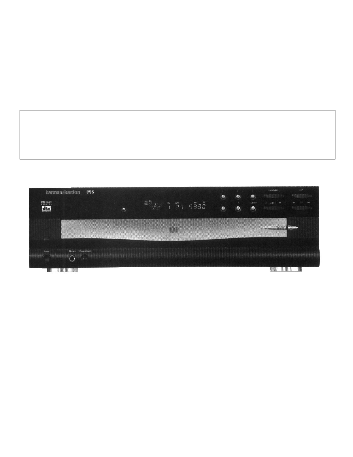
harman/kardon
FIVE DISC DVD CHANGER
PRELIMINARY
SERVICE MANUAL
DVD5
CONTENTS
PRECAUTIONS.. ……………………..….…….…….1
ESD WARNING……………………..……….……….3
SPECIFICATIONS…………………..…………...…..4
DETAILED SPECIFICATIONS……….………...…..5
FRONT PANEL CONTROLS…..…………..…….…7
INFORMATION DISPLAY………………….………..8
REAR PANEL CONNECTIONS…………………….9
REMOTE CONTROL FUNCTIONS…………….…10
INSTALLATION/CONNECTIONS…………...….…12
TROUBLESHOOTING GUIDE………………….…16
DVD5 REVISION…………………..……….……….17
harman/kardon, Inc.
250 Crossways Park Dr.
Woodbury, New York 11797
GENERAL UNIT EXPLODED VIEW (120V).…..18
GENERAL UNIT EXPLODED VIEW (230V).…..19
MECHANICAL PARTS LIST……………….….…20
TRAY/CAROUSEL EXPLODED VIEW...….……21
TRAY/CAROUSEL PARTS LEGEND...….……..22
BLOCK DIAGRAM…………………………………23
ELECTRICAL PARTS LIST………..…….….……24
IC BLOCK DIAGRAMS………….………….….....35
P.C. BOARDS…………………….……….……….55
SCHEMATIC DIAGRAMS…………….….……....63
SCHEMATIC DIAGRAMS (230v )…….….……....87
PACKING MATERIALS………..………..……..…96
Page 2
1
SERVICING PRECAUTIONS
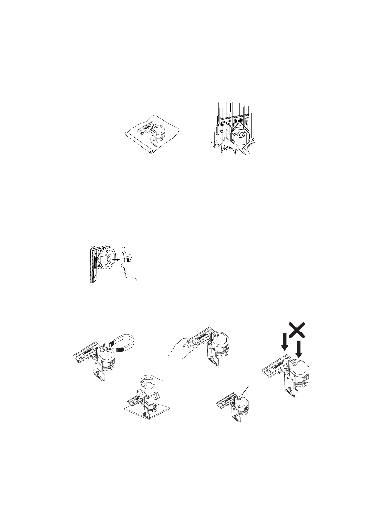
NOTES REGARDING HANDLING OF THE PICK-UP
1. Notes for transport and storage
1) The pick-up should always be left in its conductive bag until immediately prior to use.
2) The pick-up should never be subjected to external pressure or impact.
2. Repair notes
1) The pick-up incorporates a strong magnet, and so should never be brought close to magnetic materials.
2) The pick-up should always be handled correctly and carefully, taking care to avoid external pressure and
impact. If it is subjected to strong pressure or impact, the result may be an operational malfunction
and/or damage to the printed-circuit board.
3) Each and every pick-up is already individually adjusted to a high degree of precision, and for that reason
the adjustment point and installation
screws should absolutely never be touched.
4) Laser beams may damage the eyes!
Absolutely never permit laser beams to enter the eyes!
Also NEVER switch ON the power to the laser output part (lens, etc.) of the pick-up if it is damaged.
5) Cleaning the lens surface
If there is dust on the lens surface, the dust should be cleaned away by using an air bush (such as used
for camera lens). The lens is held by a delicate spring. When cleaning the lens surface, therefore, a cotton swab should be used, taking care not to distort this.
6) Never attempt to disassemble the pick-up.
Spring by excess pressure. If the lens is extremely dirty, apply isopropyl alcohol to the cotton swab. (Do
not use any other liquid cleaners, because they will damage the lens.) Take care not to use too much of
this alcohol on the swab, and do not allow the alcohol to get inside the pick-up.
Storage in conductive bag
NEVER look directly at the laser beam, and don’t let contact
fingers or other exposed skin.
Magnet
How to hold the pick-up
Conductive Sheet
Cotton swab
Pressure
Pressure
Drop impact
Page 3
2
NOTES REGARDING COMPACT DISC PLAYER REPAIRS
1. Preparations
1) Compact disc players incorporate a great many ICs as well as the pick-up (laser diode). These components are sensitive to, and easily affected by, static electricity. If such static electricity is high voltage,
components can be damaged, and for that reason components should be handled with care.
2) The pick-up is composed of many optical components and other high-precision components. Care must
be taken, therefore, to avoid repair or storage where the temperature of humidity is high, where strong
magnetism is present, or where there is excessive dust.
2. Notes for repair
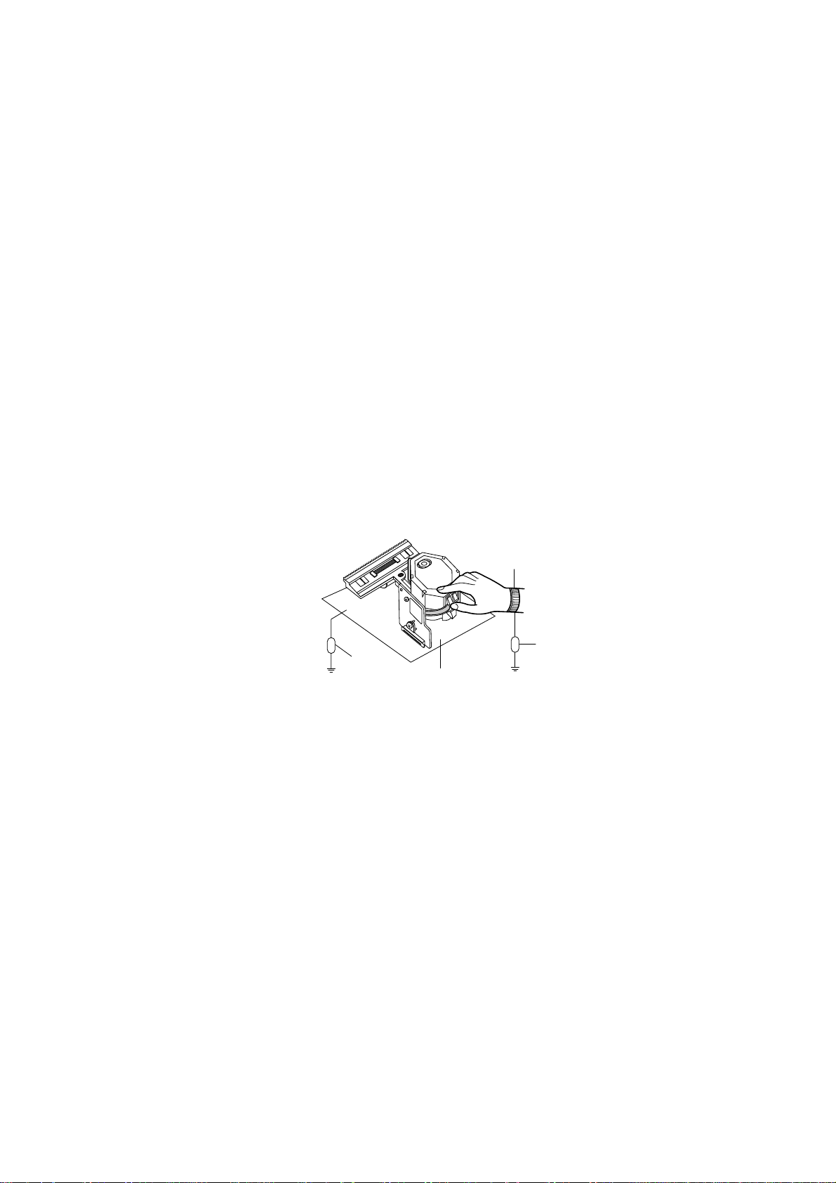
1) Before replacing a component part, first disconnect the power supply lead wire from the unit
2) All equipment, measuring instruments and tools must be grounded.
3) The workbench should be covered with a conductive sheet and grounded.
When removing the laser pick-up from its conductive bag, do not place the pick-up on the bag. (This is
because there is the possibility of damage by static electricity.)
4) To prevent AC leakage, the metal part of the soldering iron should be grounded.
5) Workers should be grounded by an armband (1MΩ)
6) Care should be taken not to permit the laser pick-up to come in contact with clothing, in order to prevent
static electricity changes in the clothing to escape from the armband.
7) The laser beam from the pick-up should NEVER be directly facing the eyes or bare skin.
Resistor
(1 Mohm)
Conductive
Sheet
Resistor
(1 Mohm)
Armband
Page 4

3
ESD PRECAUTIONS
Electrostatically Sensitive Devices (ESD)
Some semiconductor (solid state) devices can be damaged easily by static electricity. Such components commonly are called Electrostatically Sensitive Devices (ESD). Examples of typical ESD devices are integrated circuits and some field-effect transistors and semiconductor chip components. The following techniques should
be used to help reduce the incidence of component damage caused by static electricity.
1. Immediately before handling any semiconductor component or semiconductor-equipped assembly, drain off
any electrostatic charge on your body by touching a known earth ground. Alternatively, obtain and wear a
commercially available discharging wrist strap device, which should be removed for potential shock reasons
prior to applying power to the unit under test.
2. After removing an electrical assembly equipped with ESD devices, place the assembly on a conductive surface such as aluminum foil, to prevent electrostatic charge buildup or exposure of the assembly.
3. Use only a grounded-tip soldering iron to solder or unsolder ESD devices.
4. Use only an anti-static solder removal device. Some solder removal devices not classified as "anti-static"
can generate electrical charges sufficient to damage ESD devices.
5. Do not use freon-propelled chemicals. These can generate electrical charges sufficient to damage ESD
devices.
6. Do not remove a replacement ESD device from its protective package until immediately before you are
ready to install it. (Most replacement ESD devices are packaged with leads electrically shorted together by
conductive foam, aluminum foil or comparable conductive materials).
7. Immediately before removing the protective material from the leads of a replacement ESD device, touch the
protective material to the chassis or circuit assembly into which the device will by installed.
CAUTION : BE SURE NO POWER IS APPLIED TO THE CHASSIS OR CIRCUIT, AND OBSERVE ALL
OTHER SAFETY PRECAUTIONS.
8. Minimize bodily motions when handing unpackaged replacement ESD devices. (Otherwise harmless motion
such as the brushing together of your clothes fabric or the lifting of your foot from a carpeted floor can generate static electricity sufficient to damage an ESD device).
Page 5

250 Crossways Park Drive, Woodbury, New York 11797
www.harmankardon.com
© 2000 Harman Kardon, Incorporated
Part #J9020000300X
Applicable Discs: 5-inch (12cm) or 3-inch (8cm) DVD-Movie, CD or CD-RW discs
Region 1 DVD-Movie discs
DVD: Single Side/Single Layer, Single Side/Dual Layer, Dual Side/Dual Layer
Linear PCM, Dolby Digital or DTS Audio
Video Signal System: NTSC
Composite Video Output: 1V p-p/75 Ω, sync, negative polarity
S Video Output: Y/Luminance: 1V p-p/75 Ω, sync, negative polarity
C/Chrominance: 0.286V p-p
Component Video Outputs: Y: 1V p-p/75 Ω, sync, negative polarity
Pr: 0.648V p-p/75 Ω
Pb: 0.648V p-p/75 Ω
Analog Audio Output: 2.0V RMS ±0.2
Coaxial Digital Audio Output: 0.5V p-p/75 Ω
Optical Digital Audio Output: 1.6V p-p
Frequency Response: 4Hz – 22kHz ±0.5dB (48kHz sampling)
Dynamic Range: DVD: 105dB (20-bit)
CD: 100dB
Channel Separation: >90dB
THD: DVD: 0.0035%
CD: 0.0035%
Signal to Noise: >100dB
Wow & Flutter: Below measurable limits
Headphone Output: 1.2V RMS @ 32 Ω
AC Power: 120V/60Hz
Power Consumption: 25 watts
Dimensions (H x W x D): 5.1" x 17.3" x 17.2"
(130mm x 440mm x 437mm)
Weight: 15.4 lbs/7kg
Depth measurement includes knobs and buttons.
Height measurement includes feet and chassis.
All specifications subject to change without notice.
Harman Kardon is a registered trademark, and Power for the digital revolution is a trademark, of Harman Kardon, Inc.
Manufactured under license from Dolby Laboratories.“Dolby,”“Pro Logic,” “AC-3” and the Double-D symbol are trademarks of Dolby Laboratories. Confidential Unpublished Works. © 1992-2000 Dolby
Laboratories, Inc.All rights reserved.
DTS and DTS Surround are trademarks of Digital Theater Systems, Inc.
This product incorporates copyright protection technology that is protected by method claims of certain U.S. patents and other intellectual property rights owned by Macrovision Corporation and other
rights owners. Use of this copyright protection technology must be authorized by Macrovision Corporation and is intended for home and other limited viewing uses only, unless otherwise authorized by
Macrovision Corporation. Reverse engineering or disassembly is prohibited.
Technical Specifications
4
Page 6
DVD SPECIFICATIONS(PCM)
5
Page 7

DVD5 SPECIFICATIONS(DOLBY DIGITAL)
6
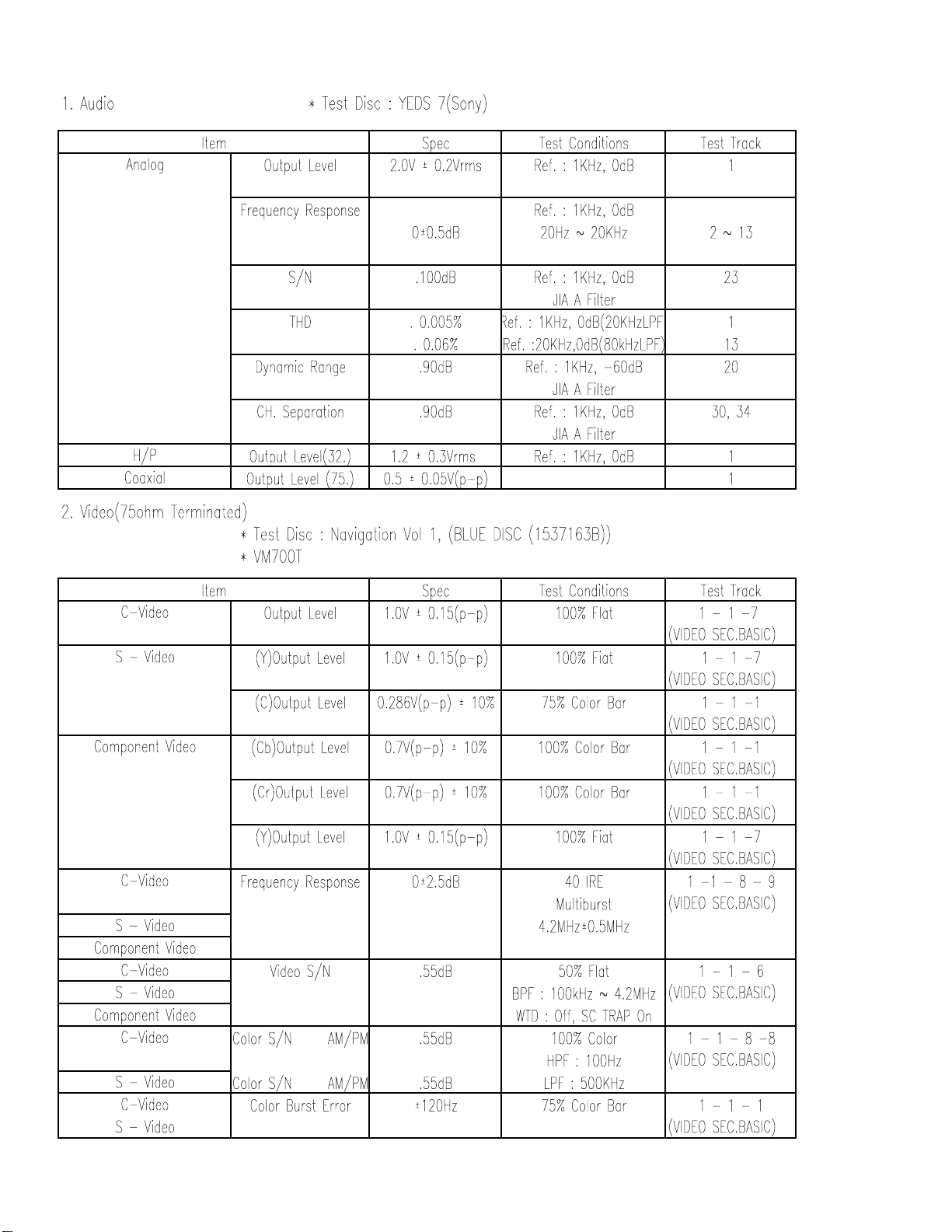
1. Audio
* Test Disc : DVD-TEST1
Item Spec Test Conditions Test
Title
Analog Output Level 2.0V ±
0.2Vrms
Ref. : 1KHz, 0dB 28
Frequency
Response
S/N 100dB 28 80Ref. : 1KHz, 0dBFS
Dynamic
Range
THD 0.005% 28Ref. : 1KHz, 0dBFS
CH. Separation 90dB 26, 27Ref. : 1KHz, 0dBFS
PLAYABILITY
0±0.5dB Ref. : Sweep 19
20Hz ~ 20KHz
-20dBFS
No Signal
JIA A Filter
100dB 13Ref. : 200Hz, -
60dBFS 20bit
JIA A Filter
LPF : 20KHz
JIA A Filter
ITEM CD
SPEC
ECCENTRICITY ±140 TCD-712 ±100 TDV-512
VERTICAL
DEVIATION
INTERRUPTION 0.6 TCD-725 0.6 TDV-521
BLACK DOT 0.6 TCD-725 0.6 TDV-525
FINGER PRINT 65 TCD-725 65 TDV-525
0.8 TCD-731 0.8 TDV-532
TEST DISC DVD
SPEC
TEST DISC
Page 8
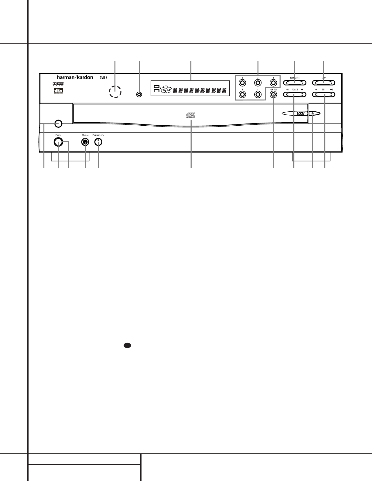
7FRONT PANEL CONTROLS
1 Master Power Switch: Press this switch
to apply power to the DVD 5. When the unit is
first turned on, the Status Indicator 3 will
turn green. Once the unit has been turned on
with this switch, it may be operated from either
the front panel or remote control. Press the
switch again to turn the unit completely off.
2 Standby Switch: Press the button once to
turn the DVD 5 on, press it again to put the
unit in the Standby mode. Note that in order for
this switch to operate, the Main Power Switch
1 must be pressed in so that it is in the
ON position.
3 Status Indicator:When the DVD 5 is in
the On mode, this indicator will glow green.
When the unit has been placed in the Standby
mode by pressing the Power-Off button
on the remote, the indicator will glow amber,
indicating that the unit is still connected to the
AC main supply and is ready to be turned on
from the remote control.
4 Headphone Jack: Connect standard head-
phones to this jack for private listening.
5 Headphone Level Control:Turn this
control to adjust the volume level to the headphones. Note that the use of this control will
not change the analog output levels at the rear
panel audio outputs.
6 Disc Tray: This tray holds as many as five
DVD or CD discs that can be played one at a
time in the DVD 5.
7 Disc Skip: Press this button to change the
disc being played. Each press of the button will
move the tray forward to the next occupied
position in the tray. Note that the unit will skip
over the empty disc positions.
8 Search Forward/Reverse: Press this but-
ton to move forward or backward through a CD
or DVD at one of four speeds. Each press and
release will increase the search speed, as indicated in the on-screen display. Once you have
selected the desired speed, release the button
and the disc will continue to search at fast
speed. To resume normal playback speed, press
the play button.
9 Open/Close Button: Press this button to
open or close the Disc T ray 6.
) Skip Forward/Reverse: Press this button
to move forward or backward through the
music tracks on a CD disc or the chapters on a
DVD disc.
! Stop: Press this button once to place the
disc in the Resume mode, which means that
playback will stop, but as long as the tray is not
opened or the disc changed, DVD playback will
continue from the same point on the disc when
the Play Button is pressed again. Resume will
also work if the unit was turned off. To stop a
disc and have play start from the beginning,
press the button twice.
@ Play/Pause: Press this button to momen-
tarily pause playback. To resume playback,
press the button again. If a DVD is playing,
action will freeze and a still picture will be
displayed when the button is pressed.
# Direct Access Buttons: Press one of
these buttons to play any of up to five discs
loaded in the Disc Tray.
$ Information Display:This display con-
tains a variety of indicators that provide information about the status of the DVD 5 and the
disc currently playing.
% Display Dim: Press this button to adjust
the brightness of the Information Display by
50% or to turn the display off completely in the
following order: FULL BRIGHTNESS ➔ HALF
BRIGHTNESS ➔ OFF ➔ FULL BRIGHTNESS.
^ Remote Sensor:The sensor that receives
the infrared commands from the remote control
is behind this area. Do not cover or obscure this
part of the front panel in order to avoid a malfunction with the remote.
Front Panel Controls
1 Master Power Switch
2 Standby Switch
3 Status Indicator
4 Headphone Jack
5 Headphone Level Control
6 Disc Tray
7 Disc Skip
8 Search Forward/Reverse
9 Open/Close Button
) Skip Forward/Reverse
! Stop
@ Play/Pause
# Direct Access Buttons
$ Information Display
% Display Dim
^ Remote Sensor
/
RESUME
TITLE
RANDOM
CHAPTER
REPEAT
TRACK
1ALL
HOUR
DISC
A – B
MIN
PROG.
INTRO
SEC
DVD
CD
—±‚
1
2
3
4
5
DISC
1
2
3
4
5
6
7
8
9
)
!
@
#
$
%
^
29
Page 9
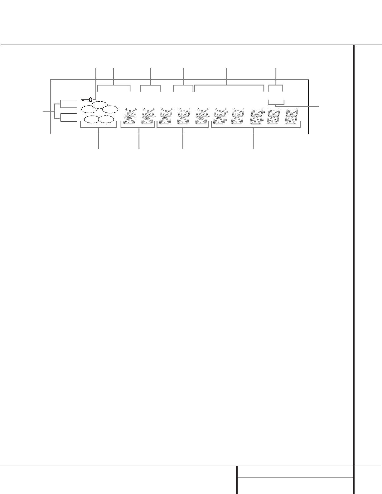
8 FRONT PANEL INFORMATION DISPLAY
Front Panel Information Display
RESUME
TITLE
RANDOM
CHAPTER
REPEAT
TRACK
1ALL
HOUR
DISC
A – B
MIN
PROG.
INTRO SEC
DVD
CD
—±‚
1
2
3
4
5
DISC
A
B
C
D
E
F
L
K
J
IH G
A Disc Type Indicators
B Disc-Number Indicators
C Title Indicators
D Chapter/Track Number Indicators
E Program Time Indicators
F Intro Indicator
G Program Indicator
H Repeat Indicators
I Random Indicator
J Resume Indicator
K Playback-Mode Indicators
L Parental Lock Indicator
A Disc Type Indicators: The DVD or CD
indicator will illuminate to show the type of
disc currently being played.
B Disc-Number Indicators:When the
DVD 5 has sensed that a disc is loaded in one
or more of the tray positions, the number inside
the corresponding disc icon will illuminate.The
disc position that is currently playing will flash.
Note that if a disc is added to, or removed
from, the tray while a disc is playing, the
indicator will not show the change until all
discs are cycled.
C Title Indicators:These two positions in
the display will show the current title number
when a DVD disc is playing.
D Chapter/Track Number Indicators:
When a DVD disc is playing, these two positions in the display will show the current chapter. When a CD disc is playing they will show
the current track number.
E Program Time Indicators:These posi-
tions in the indicator will show the running
time of a DVD in play.When a CD is playing,
these indicators will show the current track
time, time remaining in the current track, or the
total remaining time on the disc.
NOTE: The Program Time Indicators will also
display text messages about the DVD 5’s status,
including Reading when a disc is loading,
Bye when the unit is turned off, and Disc
Error when a disc not compatible with the
DVD 5 is put into the play position.
F Intro Indicator:This indicator lights when
the Intro Scan function is active.
G Program Indicator:This indicator lights
when the programming functions are in use.
H Repeat Indicators:These indicators light
when any of the Repeat functions are in use.
I Random Indicator:This indicator lights
when the unit is in the Random Play mode.
J Resume Indicator:This indicator lights
when the Stop button has been pressed once
to put the unit in the Resume mode.
K Playback-Mode Indicators:These indica-
tors light to show the current playback mode:
› Lights when a disc is playing in the normal
mode
›› Lights when the disc is in the Fast Search
Forward mode. For DVDs,When both triangles
glow steadily, the disc plays at 2x normal
speed. When the right triangle is flashing, the
disc plays at 4x normal speed. When the left
triangle is flashing, the disc plays at 8x normal
speed. When both triangles are flashing, the
disc plays at 16x normal speed. For CDs, only
the first three Fast Search modes are available.
›± Lights when the disc is paused
‹‹ Lights when the disc is in the Fast Search
Reverse mode. For DVDs, When both triangles
glow steadily, the disc plays at 2x normal
speed. When the left triangle is flashing, the
disc plays at 4x normal speed. When the right
triangle is playing, the disc plays at 8x normal
speed. When both triangles are flashing, the
disc plays at 16x normal speed. For CDs, only
the first three Fast Search modes are available.
L Parental Lock Indicator: This indicator
lights when the parental-lock system is
engaged in order to prevent anyone from
changing the rating level without a code.
Page 10
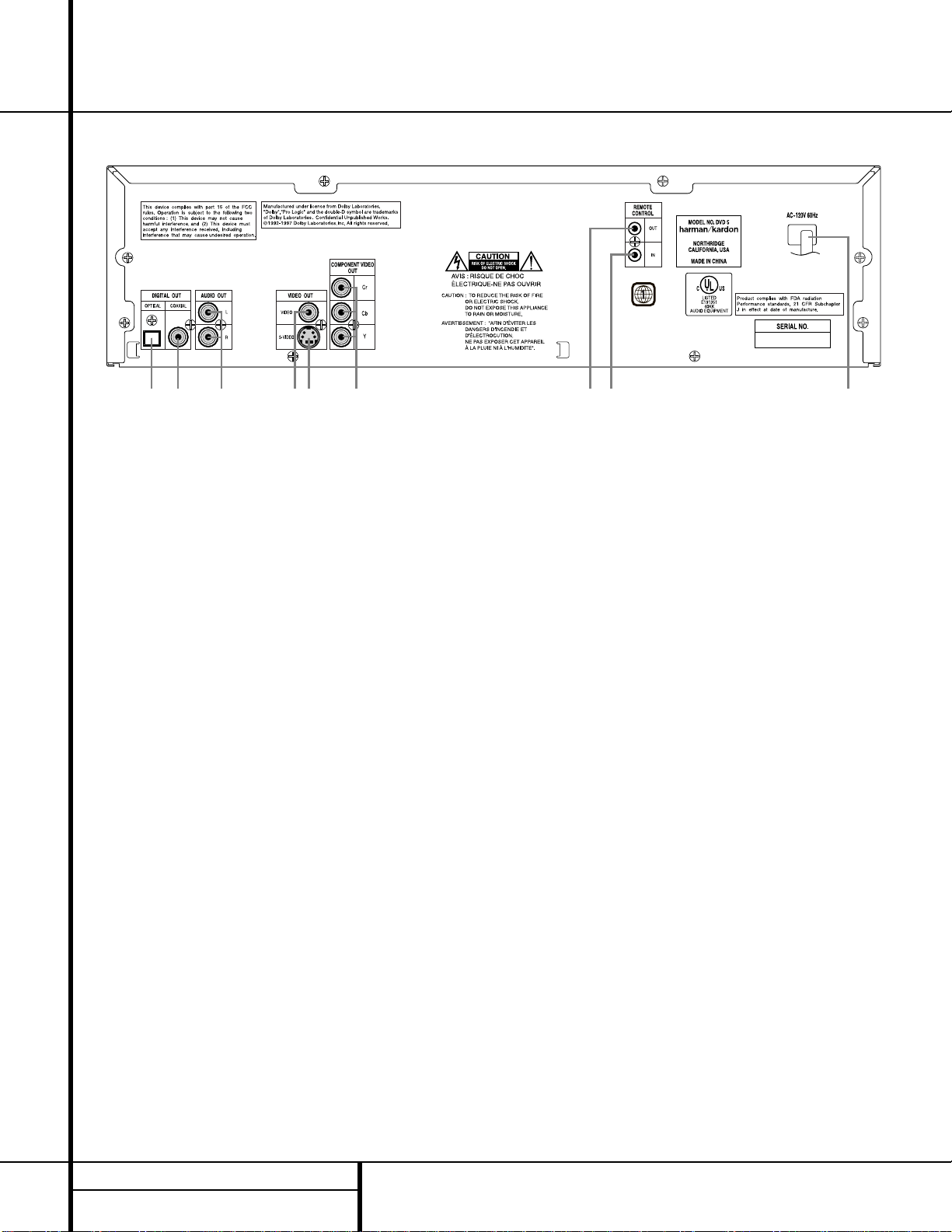
Rear Panel Connections
¡ ™
£
¢
∞
§
¶ •
ª
¡ Optical Digital Output
™ Coaxial Digital Output
£ Analog Audio Outputs
¢ Composite Video Output
∞ S-Video Output
§ Component Video Outputs
¶ Remote Control Output
• Remote Control Input
ª AC Power Cord
REAR PANEL CONNECTIONS
¡ Optical Digital Output: Connect this jack
to the optical digital input of an A/V receiver or
surround processor for Dolby Digital, DTS or
PCM audio playback.
™ Coaxial Digital Output: Connect this jack
to the coaxial digital input of an A/V receiver or
surround processor for Dolby Digital, DTS or
PCM audio playback.
NOTE:The coaxial digital output should only be
connected to a digital input. Even though it is
the same RCA-type connector as standard analog audio connections, DO NOT connect it to a
conventional analog input jack.
£ Analog Audio Outputs: Connect these
jacks to an audio input on an A/V receiver or
surround processor for analog audio playback.
¢ Composite Video Output: Connect this
jack to the video input on a television or video
projector, or to a video input on an A/V receiver
or processor if you are using that type of device
for video input switching.
∞ S-Video Output:Connect this jack to the
S-Video input on a television or video projector,
or to an S-Video input on an A/V receiver or
processor if you are using that type of device
for S-Video input switching.
§ Component Video Outputs: If your TV or
video projector has component video inputs,
you may connect these output jacks to the set
for the highest video quality available. Note
that the component video inputs may be
labeled as Y/Pr/Pb or Y/Cr/Cb but, for connection purposes, they are the same. The outputs
of these jacks should NOT be connected to a
standard composite video input.
¶ Remote Control Output:Connect this
jack to the infrared (IR) input jack of another
compatible Harman Kardon remote controlled
product to have the built-in Remote Sensor ^
on the DVD 5 provide IR signals to other
compatible products.
• Remote Control Input:Connect the out-
put of a remote infrared sensor, or the remote
control output of another compatible Harman
Kardon product, to this jack.This will enable
the remote control to operate even when the
front panel Remote Sensor ^ is blocked. This
jack may also be used with compatible IR
remote control-based automation systems.
ª AC Power Cord: Connect this plug to an
AC outlet. If the outlet is controlled by a switch,
make certain that it is in the ON position.
9
Page 11
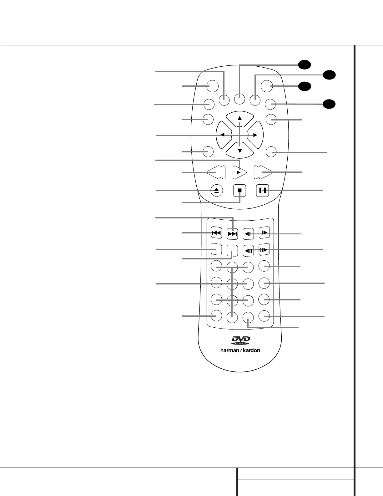
REMOTE CONTROL FUNCTIONS
●
●
●
●
Remote Control Functions
a Audio Button
b Power-On Button
c Mode Button
d Enter Button
e Navigation Buttons
f Return Button
g Play Button
h Reverse Search Button
i Open/Close Button
j Stop Button
k Next Button
l Previous Button
m Random Button
n Disc-Skip Button
o Numeric Keys
p Repeat Button
q Repeat A-B Button
r Light Button
s Clear Button
t Check Button
u Program Button
v Step Buttons
w Slow-Play Buttons
x Pause Button
y Forward Search Button
z Subtitle On/Off Button
` Menu Button
28
Title Button
29
Power-Off Button
30
Angle Button
31
Subtitle Button
32
3
a Audio Button:When a DVD is playing,
press this button to select from the available
audio tracks or languages on the disc.
b Power-On Button: Press this button to turn
the DVD 5 on. Note that in order for this control
to function, the Front Panel Main Power Switch
1 must first be pressed in, so that the unit is in
the Standby mode.
c Mode Button:When a disc is playing,
pressing the button will display the Status Banner
which contains information about the disc and
enables you to change the functions.
d Enter Button:Press this button to select
the item that is highlighted in the DVD 5’s Status
Banner or in the on-screen menu displayed by a
DVD disc.
10
a
c
e
g
i
k
m
o
b
d
f
h
j
l
n
p
POWER
ON
MODE
ENTER
RETURN
SEARCH
OPEN/CLOSE
RANDOM
REPEAT
AUDIO
PREV.
1
4
7
SUBTITLE
PLAY
STOP
NEXT
DISC SKIP
23
5
8
0
6
9
A - B
ANGLE
SLOW
STEP
POWER
OFF
SEARCH
PAUSE
PROG.
CHECK
CLEAR
LIGHT
TITLE
MENU
SUBTITLE
ON/OFF
31
30
29
28
`
z
y
x
w
v
u
t
s
r
q
DVD 5 RC
Page 12

11 REMOTE CONTROL FUNCTIONS
Remote Control Functions
e Navigation Buttons:Press these buttons
to change or select an item from the DVD 5’s
Status Banner or in the on-screen menu
displayed by a DVD disc.
f Return Button:When viewing the menu
display from a DVD disc, press this button to
return to the previous menu screen.
g Play Button:Press this button to begin
playback. If the disc tray drawer is open, it will
automatically close when the button is pushed.
Pressing the Play button when the unit is in the
Standby mode will turn the unit on and begin
playback of the last disc in use.
h Reverse Search:Press this button to
move backward through a CD or DVD at one
of four speeds. Each press and release will
increase the search speed, in the following
order: R. Search x 2 ➔ R. Search x 4 ➔
R. Search x 8 ➔ R. Search x 16. Once you have
selected the desired speed, release the button,
and the disc will continue to search at fast
speed. To resume normal playback, press the
Play Button g.
i Open/Close Button: Press this button to
open or close the disc tray drawer. If the drawer
is opened while a disc is still playing, playback
will continue and discs not in use may be
changed. If the drawer is opened while the
unit is stopped, the disc that was playing will
be presented at the front-center position of
the tray.
j Stop Button: Press this button once to
place the disc in the Resume mode, which
means that playback will stop; as long as the
tray is not opened or the disc changed, DVD
playback will continue from the same point on
the disc when the Play Button g is pressed
again. Resume will also work if the unit is
turned off.To totally stop a disc, press the
button twice.
k Next Button: Press this button to move
forward through the music tracks on a CD disc
or the chapters on a DVD disc.
l Previous Button:Press this button to
move backward through the music tracks on a
CD disc or the chapters on a DVD disc.
m Random Button: Press this button to
begin the playback of all tracks on a disc in
random order.
n Disc-Skip Button: Press this button to
move to the next available disc in the tray.
o Numeric Keys: Press these keys to enter
data for sequential programming, to enter or
change the access password for parental control, to enter a language code, or to respond to
menu options presented by a disc.
p Repeat Button: Press this button to
select a Repeat-Play mode. Each press of the
button shows the choice selected in either the
on-screen Status Banner display or in the
Repeat Indicators H.
q Repeat A-B Button: Press this button
once to begin the selection of a portion of a
disc to be repeated. Press it again to choose the
end point of the repeat-play selection.
r Light Button: Press this button to acti-
vate the remote’s backlighting so that the keys
are visible in low-light conditions.
s Clear Button: Press this button to remove
the Status Banner or other displays from your
video screen. This button is also used to
clear items from Programmed Play lists.
(See page 29.)
t Check Button:When a CD is playing,
press this button to check the status of the
current disc via the on-screen display.This
button is also used to verify the contents of a
programmed play list via the front panel
Information Display. (See page 28 for more
information about programming the DVD 5.)
u Program Button:When the unit is
stopped, press this button to display the
program menu and enter a programmed play
sequence.When a disc is playing, press this
button to switch between normal play and
programmed playback.
v Step Buttons:When a DVD disc is play-
ing, press these buttons to move forward or
backward one frame at a time. Press the Play
Button g/@ to resume normal play. These
buttons do not function when a CD is playing.
w Slow-Play Buttons:When a DVD disc is
playing, press these buttons to move forward or
backward through the disc in slow speed. Each
press of these buttons changes the slow-play
speed in the following order: 1/16 Normal
Speed ➔ 1/8 Normal Speed ➔1/4 Normal
Speed ➔ 1/2 Normal Speed.
To resume normal play, press the Play Button
g/@. These buttons do not function when a
CD is playing.
x Pause Button: Press this button to stop
the disc in use.To resume playback, either press
the Pause Button again or press the Play
Button g/@.
y Forward Search: Press this button to
move forward through a CD or DVD at one of
four speeds. Each press and release will
increase the search speed, in the following
order: F. Search x 2 ➔ F. Search x 4 ➔
F. Search x 8 ➔ F. Search x 16. Once you have
selected the desired speed, release the button
and the disc will continue to search at fast
speed. To resume normal playback speed, press
the play button.
z Subtitle On/Off Button:When a DVD is
playing, press this button to turn the subtitle
display on or off.
` Menu Button:This button has two func-
tions.When a DVD disc is playing, press this
button to stop the disc playback and display the
DVD’s main menu screen for the current title.
When the unit is stopped, press this button to
display the Setup Menu.
Title Button: When a DVD disc is play-
ing, press this button to display the disc’s Title
Select Menu. If the disc does not offer this function, a symbol (X) will appear on the screen to
indicate that there is only one title on the disc
or that the disc does not allow this feature.
Power-Off Button: Press this button to
place the unit in the Standby mode.
Angle Button: When a DVD encoded
with multiple-angle information is playing, press
this button to change the angle in use. Note
that this function is only available on discs that
are specially prepared to take advantage of the
multiple-angle function, and only for those
parts of the disc that are recorded with
multiple-angle content. The DVD 5 will display a
camera icon on the screen to indicate when this
feature is available.
Subtitle Button: When a DVD disc is
playing, press this button to change the subtitle
choice.To actually turn the subtitles on or off,
press the Subtitle On/Off Button z.
31
30
29
28
Page 13

12 INSTALLATION AND CONNECTIONS
Installation
Connections will vary, depending on the type of
audio and video components used with your
DVD 5. However, regardless of the complexity
of your system, the installation guidelines on
pages 11–14 should always be followed to
ensure a safe installation and reliable operation
of the product.
Important Note: To prevent possible damage
to your speakers or other components in your
home entertainment system, we strongly recommend that ALL system components, including the DVD 5, be turned off and unplugged
from their AC power source when any connections are made or a new component is
installed.
Placement of the DVD 5
Since the laser transport mechanism and
carousel tray in the DVD 5 are precision instruments that are designed and manufactured to
precise tolerances, they are subject to interference from vibration. To minimize the possibility
of skipping during playback, it is recommended
that the unit be placed on a level, solid,
vibration-free surface.
When installing the DVD 5 in a cabinet or tight
space, always make certain that there is enough
room in front of the unit for the disc tray to
open fully, and that there is enough space
above the unit so that discs may easily be
inserted into the spaces in the tray.
As the disc drawer extends out about six inches
from the front of the unit when it is open, you
should also make certain that there is sufficient
clearance in front of the unit to accommodate
the disc drawer without it bumping into other
objects or getting in the way of anyone walking
in front of the unit.
In addition to the safety considerations outlined
on page 4, it is also recommended that the
DVD 5 not be placed in a location that is subject to direct sunlight or extreme heat or cold,
as these conditions may damage the discs used
in the player, or the player itself. Note that
audio amplifiers or high-power receivers, as
well as certain other electronic products, can
generate significant heat. For that reason, do
not place the DVD 5 directly on top of an
amplifier, receiver, or other heat source.
Always allow at least one inch of free space on
all sides of the DVD 5 as well as around other
electronic products to allow for proper
ventilation.
Installation Options
The diagrams on pages 12–14 describe the
three basic ways to connect the DVD 5 to your
system components.
■ Option #1: Use this setup if all audio and
video connections from the DVD 5 will go
directly to a television set or video projector
without the use of an A/V receiver or
surround processor.
■ Option #2: Use this setup if the video con-
nections will go directly to a television set or
video projector, but the audio connections
will be made to an A/V Receiver or surround
processor.
■ Option #3: Use this setup if all audio and
video connections will be made through an
A/V receiver or a surround processor.
Installation and Connections
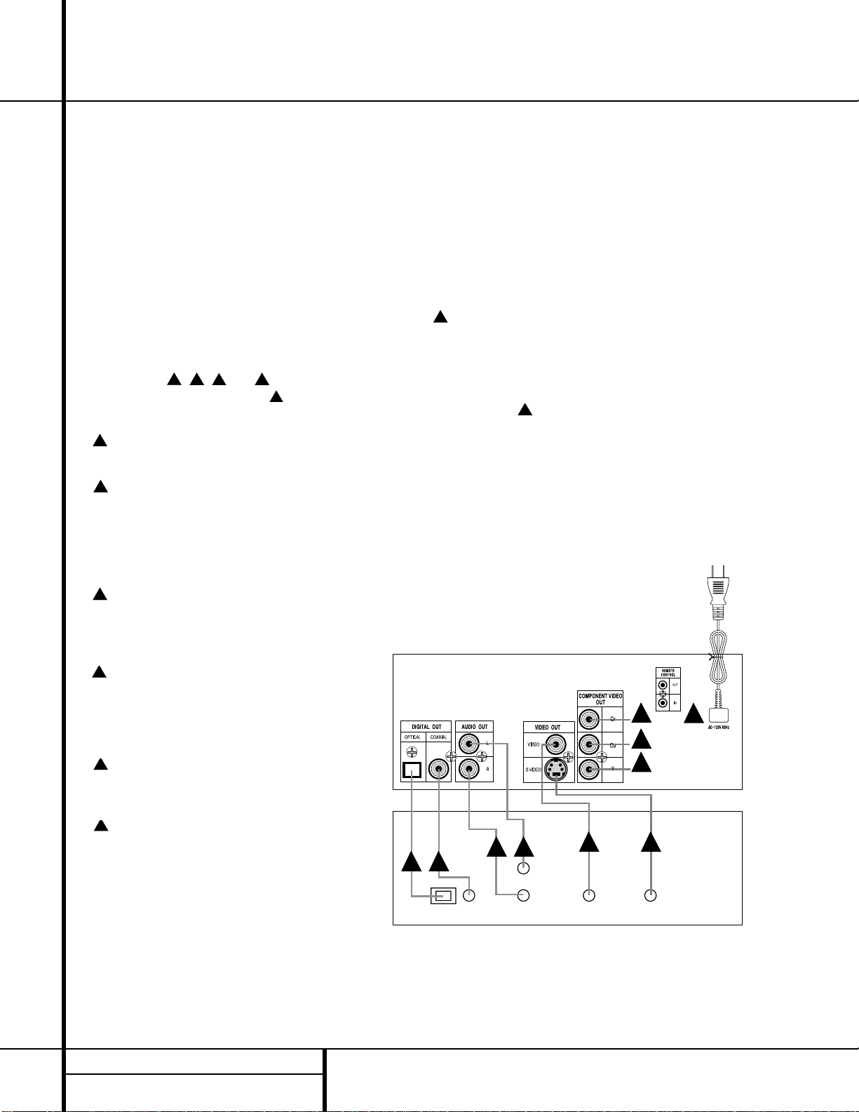
Page 14
13 INSTALLATION AND CONNECTIONS
Installation and Connections
OPTION 1:
Direct Connections to a Television or
Video Projector
This is the simplest installation, as it does not
require anything other than a television set.
However, note that in this type of system you
will not be able to enjoy the benefits of Dolby
Digital or DTS discrete playback, as that
requires the digital audio processing found in
A/V receivers or surround processors. Follow as
many of these steps as needed, based on the
capabilities of your television:
Connect the left and right
Analog Audio
Outputs
£ on the DVD 5 to the audio
inputs on your television. Connect the
Composite Video Output ¢ on the DVD 5
to a video input on your television. Note that
composite video connections typically have a
yellow center ring for easy identification.
If your television or projector is equipped
with component video inputs, connect the three
Component Video Outputs § on the DVD
5 to the matching component video inputs on
your video display.
Connect the
S-Video Output ∞ on the
DVD 5 to an S-Video input on your television.
Connect the AC power cord to an AC
outlet.
Installation Notes and Hints
■ If your television has both standard compos-
ite video and S-Video inputs, you only need
to use one of the two connections.Where
possible, we recommend using the S-Video
connection due to the higher picture quality.
■ Do not connect any of the video outputs of
the DVD 5 through a VCR. Due to the use of
Macrovision encoding on most DVD discs,
connections through the circuitry of a VCR
will distort the picture so that it will become
unwatchable.
■ Note that the volume level for DVD playback
may different from the level for TV broadcasts.This is normal and does not indicate a
problem with the DVD 5 or your TV set.
Simply use the volume control on the TV set
to set the desired level.
■ Depending on the product and brand, a
number of different descriptions are used to
label component video connections.You may
see them as Y/Pr/Pb, Y/Cr/Cb or Y/R-Y/B-Y.
For the purpose of connecting a DVD player,
all of these labels are normally identical. The
best guide is to connect the component
video connections using the green/red/blue
color coding of the inner rings of the connection jacks.
■ When making connections to a high defini-
tion (HDTV) or “digital ready” set, do not
connect the component video outputs of the
DVD 5 to inputs labeled “HD Component
Inputs” unless you have checked with the
set’s owner’s manual to ensure that the HD
input is also compatible with standard scan
(NTSC) video.
A
C
B
TV
D
E
A B C D
L R
E
DVD 5
Page 15
14 INSTALLATION AND CONNECTIONS
OPTION 2:
Direct Connections to a Television or
Video Projector with Audio Connections
to an A/V Receiver or Surround Processor
To hear the benefits of discrete, multichannel
digital audio, you will need to use an external
Dolby Digital/DTS-capable A/V receiver or
surround processor. In this installation, you
maintain a direct video connection to your
television, but use the audio processing from
another device.
Note that step is not used, as it is for
analog audio connections only.This installation
starts with step
Connect the
Composite Video Output
¢ on the DVD 5 to a video input on your television. Note that composite video connections
typically have a yellow center ring for easy
identification.
If your television or projector is equipped
with component video inputs, connect the three
Component Video Outputs§ on the DVD
5 to the matching component video inputs on
your video display.
Connect the
S-Video Output ∞ on the
DVD 5 to an S-Video input on your television.
Connect the AC power cord to an AC
outlet.
Connect either the
Optical Digital
Output
¡ or the Coaxial Digital Output
™ on the DVD 5 to the matching digital input
jacks on your A/V receiver or surround processor. Note that only one of these connections is
required, not both.
Connect the left/right
Analog Audio
Outputs
£ of the DVD 5 to the matching
left/right analog inputs on your A/V receiver or
surround processor.
Installation Notes and Hints
■ Only one type of audio connection is
required, either digital or analog. If possible,
a digital connection is preferred, as that will
enable you to listen to DVD soundtracks
with the clarity, definition and channel separation made possible by Dolby Digital and
DTS. Follow Step for digital audio connections. However, if you do not yet have a
receiver capable of digital audio processing,
you will still benefit from an analog connection so that the receiver may create a multichannel soundfield using Dolby Pro Logic or
other matrix decoding. Follow Step for
instructions on analog audio connections.
■ If your television has both standard compos-
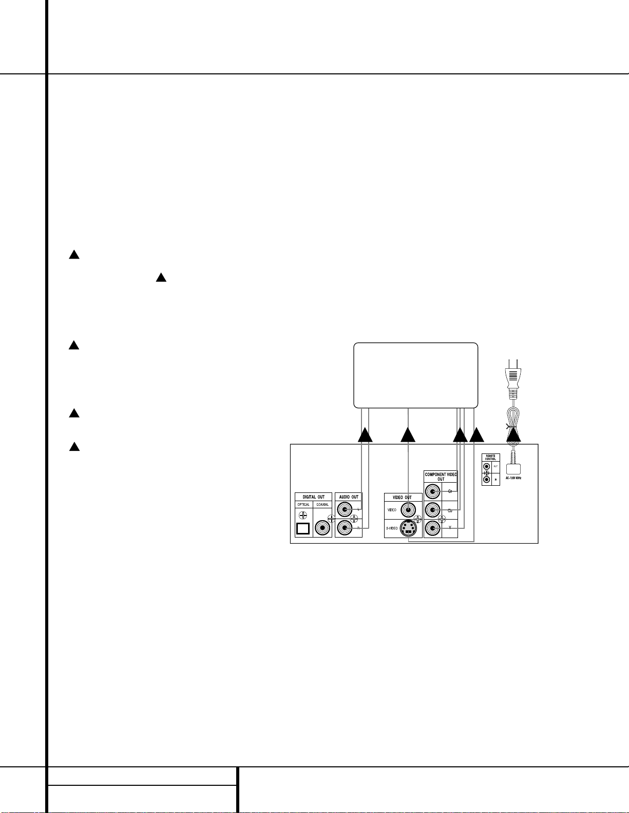
ite video and S-Video inputs, you only need
to use one of the two connections.Where
possible, we recommend an S-Video connection due to the higher picture quality.
■ Do not connect any of the video outputs of
the DVD 5 through a VCR.The use of
Macrovision encoding on most DVD discs
means that most discs will have a distorted
picture when connections are made through
a VCR.
■ Note that the volume level for DVD playback
may different from the level for other input
sources to your receiver. This is normal and
does not indicate a problem with the DVD 5
or your receiver. Simply use the volume control on the receiver to set the desired level.
■ Depending on the product and brand, a
number of different descriptions are used to
label component video connections.You may
see them as Y/Pr/Pb, Y/Cr/Cb or Y/R-Y/B-Y.
For the purposes of connecting a DVD player, all of these labels are normally identical.
The best guide is to connect the component
video connections using the green/red/blue
color coding of the inner rings of the connection jacks.
■ When making connections to a high defini-
tion (HDTV) or “digital ready” set, do not
connect the component video outputs of the
DVD 5 to inputs labeled “HD Component
Inputs” unless you have checked with the
set’s owner’s manual to ensure that the HD
input is also compatible with standard scan
(NTSC) video.
Installation and Connections
A
B
B
C
F
G
D
E
F
G
F F
G G
Audio In
TV
B C
Receiver
D
DVD 5
E
Digital In
Page 16
15 INSTALLATION AND CONNECTIONS
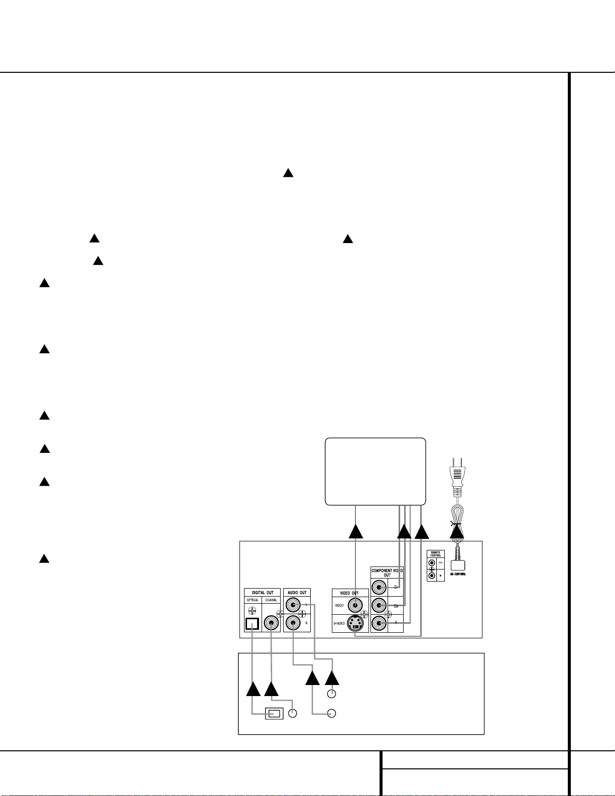
OPTION 3:
Audio and Video Connections through an
A/V Receiver or Surround Processor only
If your home entertainment system has other
audio/video input sources in addition to the
DVD 5, such as a VCR, cable set-top box or
satellite receiver, LD player, personal video
recorder or HDTV tuner, the most efficient way
to manage the various components is to make
all audio/video connections through an A/V
receiver or surround processor. This simplifies
the selection of an input source, and allows
many different components to be connected to
the same video display and speakers.
Note that steps / / and are not
used. This installation starts with step
Connect the AC power cord to an AC
outlet.
Connect either the
Optical Digital
Output
¡ or the Coaxial Digital Output
™ on the DVD 5 to the matching digital input
jacks on your A/V receiver or surround processor. Note that only one of these connections is
required, not both.
Connect the left/right
Analog Audio
Outputs
£ of the DVD 5 to the matching
left/right analog inputs on your A/V receiver or
surround processor.
Connect the
Composite Video Output
¢ on the DVD 5 to a video input on your
receiver or processor. Note that composite video
connections typically have a yellow center ring
for easy identification.
Connect the
S-Video output ∞ on the
DVD 5 to an S-Video input on your receiver or
processor.
If your television or projector is equipped
with component video inputs, connect the three
Component Video Outputs § on the
DVD 5 to the matching component video inputs
on your video display. However, if your receiver
or processor has multiple component input
switching capability, connect the
Component
Video Output Jacks
∞ on the DVD 5 to the
matching component video inputs on your
receiver, surround processor or video processor.
Installation Notes and Hints
■ For this installation, make the connections
from the receiver or processor to your video
display and speakers as described in the
owner’s manuals for those products.
■ Only one type of audio connection is
required, either digital or analog. If possible,
a digital connection is preferred as that will
enable you to listen to DVD soundtracks
with the clarity, definition and channel separation made possible by Dolby Digital and
DTS. Follow Step for digital audio connections. However, if you do not yet have a
receiver capable of digital audio processing,
you will still benefit from an analog connection so that the receiver may create a multichannel soundfield using Dolby ProLogic or
other matrix decoding. Follow Step for
instructions on analog audio connections.
■ If your television has both standard compos-
ite video and S-Video inputs, you only need
to use one of the two connections.Where
possible, we recommend an S-Video connection due to the higher picture quality.
■ Do not connect any of the video outputs of
the DVD 5 through a VCR.The use of
Macrovision encoding on most DVD discs
means that most discs will have a distorted
picture when connections are made through
a VCR.
■ Note that the volume level for DVD playback
may different from the level for other input
sources to your receiver. This is normal and
does not indicate a problem with the DVD 5
or your receiver. Simply use the volume control on the receiver to set the desired level.
■ Depending on the product and brand, a
number of different descriptions are used to
label component video connections.You may
see them as Y/Pr/Pb, Y/Cr/Cb or Y/R-Y/B-Y.
For the purposes of connecting a DVD player, all of these labels are normally identical.
The best guide is to connect the component
video connections using the green/red/blue
color coding of the inner rings of the connection jacks.
■ When making connections to a high defini-
tion (HDTV) or “digital ready” set, do not
connect the component video outputs of the
DVD 5 to inputs labeled “HD Component
Inputs” unless you have checked with the
set’s owner’s manual to ensure that the HD
input is also compatible with standard scan
(NTSC) video.
Installation and Connections
A/V Receiver or Surround Processor
BCD
E
J
J
J
Audio In
Video In S-Video In
Digital In
DVD 5
F F
G G
H I
A
B
C
E
D
E
F
G
F
G
H
I
J
Page 17

16 TROUBLESHOOTING GUIDE
Troubleshooting Guide
TROUBLESHOOTING GUIDE
SYMPTOM POSSIBLE CAUSE SOLUTION
Unit does not turn on • Main Power Switch turned Off • Press in Main Power Switch
• No AC power • Check AC power plug and make certain any switched
outlet is turned on
Disc does not play • Disc loaded improperly • Load disc label-side up
• Incorrect disc type • Check to see that disc is CD, CD-RW or DVD-Movie;
• Invalid Region Code other types will not play
• Rating is above parental preset • Use Region 1 disc only
• Enter password to override or change rating settings
No picture • Intermittent connections • Check all video connections
• Wrong Input • Check input selection of TV or reveiver
No sound • Intermittent connections • Check all audio connections
• Incorrect digital audio selection • Check digital audio settings
• DVD disc is in fast or slow mode • There is no audio playback on DVD discs during
fast or slow modes
Picture is distorted or jumps during • MPEG-2 decoding • It is a normal artifact of DVD playback for pictures
fast forward or reverse play to jump or show some distortion during rapid play
Some remote buttons do not operate • Function not available for this disc • Some discs do not include all DVD features
during DVD play
The menu is in a foreign language • Incorrect menu language • Change menu language selection
“X” Symbol Appears • Requested function not available at • Certain functions may be disabled during passages
this time of a disc
Picture is displayed in the wrong aspect ratio • Incorrect match of aspect ratio settings • Change Aspect Ratio settings
to disc
Remote control inoperative • Weak batteries • Change both batteries
• Sensor is blocked • Clear path to sensor or use remote sensor
Disc will not copy to VCR • Macrovision protection • Most DVDs are encoded with Macrovision
to prevent copying to VCR
K
SUBJECT: RESET DVD5 TO FACTORY DEFAULTS, RESETTING PARENTAL LOC
In Stand-by mode, press SEARCH BACK and SKIP FORWARD buttons on the Front
Panel simultaneously for more than 3 seconds.
The FL will then display 8 or 9 digit numbers. Disregard this read out. Reset the unit by
pressing the OFF power button on the remote, or pushing the main power button on the
unit.
Page 18

Harman/kardon
17
DVD5 REVISIONS
Product Information
Product:
Serial Number:
Failure Description
System Setup: --include equipment connected, speakers used, cable connections, etc.
Unit playing The Man with the Golden Gun, Special 007 Edition, Digital Coax Output to AVR, Composite Video Out to AVR or
Unit playing the above DVD using, Analog Audio, Composite Video Out directly to TV.
Failure Mode: --include source (AM/FM, DVD, etc.), surround mode, volume level, and channels affected.
During Chapter 21 of The Man with the Golden Gun, Special 007 Edition, at a time of 1:21:23, a brief video pause is seen, and
then the audio and video becomes severel y distorted. The distortion occurs throughout the remainder of the disc. The problem was
also recreated on an engineering sample DVD5.
DVD5
Verified on Reliability Qualification unit manufactured in February 2000
Analysis
Results:
The DVD is a 2-layer DVD. It is believed that the point at which the problem occurs is at the transition (layer break) to layer 2. If
this is the case, then the DVD5 has a problem reading layer 2 of the disc. Further analysis of DVD5 and of the material is needed
to determine the exact cause of this failure.
6/30/00: We have recreated the problem and have determined that the problem is due to a failure of the ST chipset. All DVD
players using the ST chipset have the same problem. Software Version 1.54 will correct the problem.
Describe Problem ECN #24
1), Issue the latest software version to resolve: DVD can’t play 2 layer disc.
2), Improve remote control sensitivity issue,
change R985 from 3.9k ohm to 10k ohm.
Identify & Verify Root
Cause
Choose & Verify
Permanent Corrective
Action
Serial Numbers TH0007-09598 and later for DVD5 - US 120v version
DVD5.0 has a problem reading layer 2 of the disc
Update new software(software version 1.55) to correct.
NOTE: FOR SOFTWARE UPGRADES ALL UNITS MUST BE SENT TO:
EUROPEAN HI-TECH
25930 BELLEPORTE AVE
HARBOR CITY, CA. 90710
Page 19
18
120v
Page 20
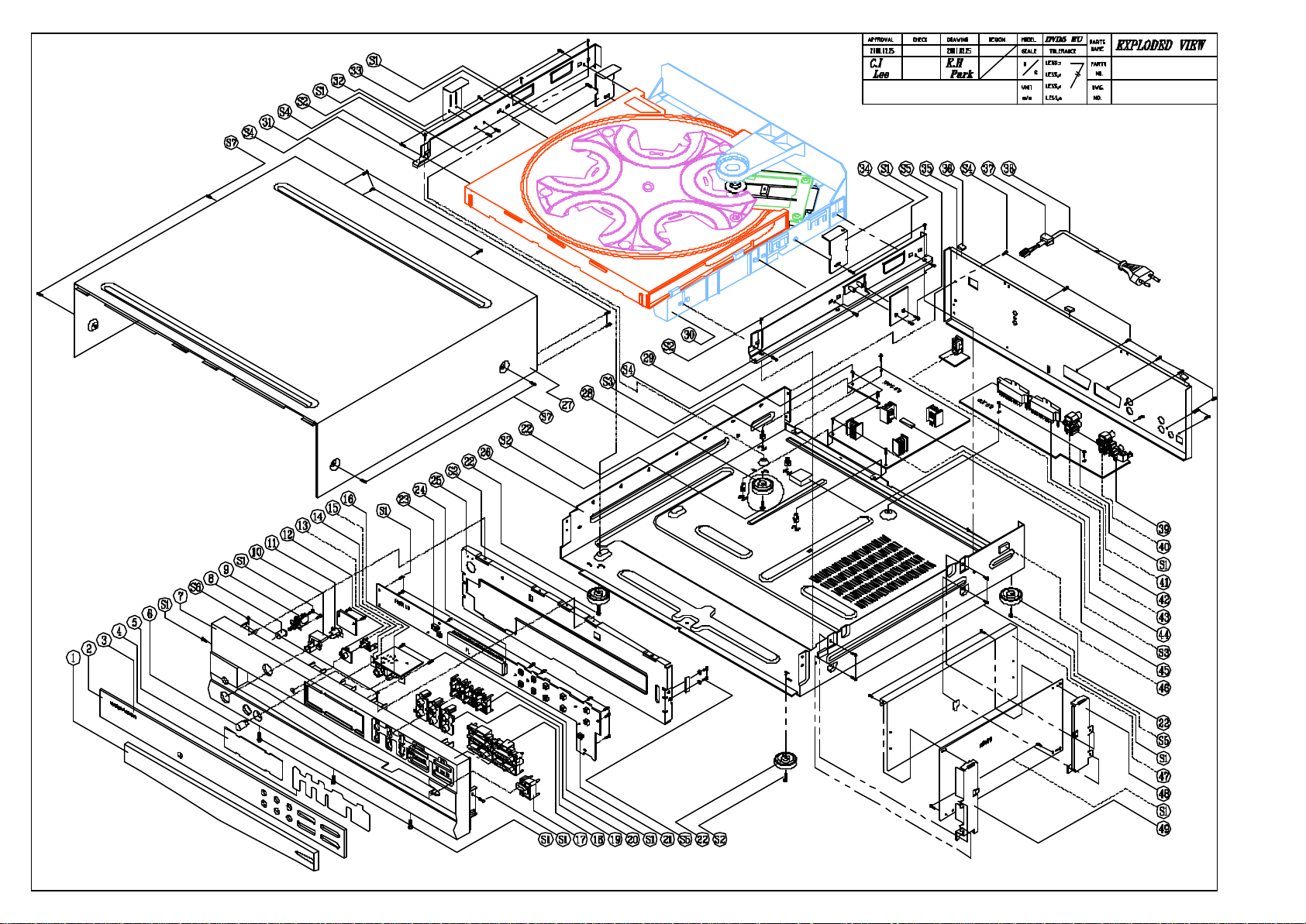
19
230v
C
B
A
Page 21

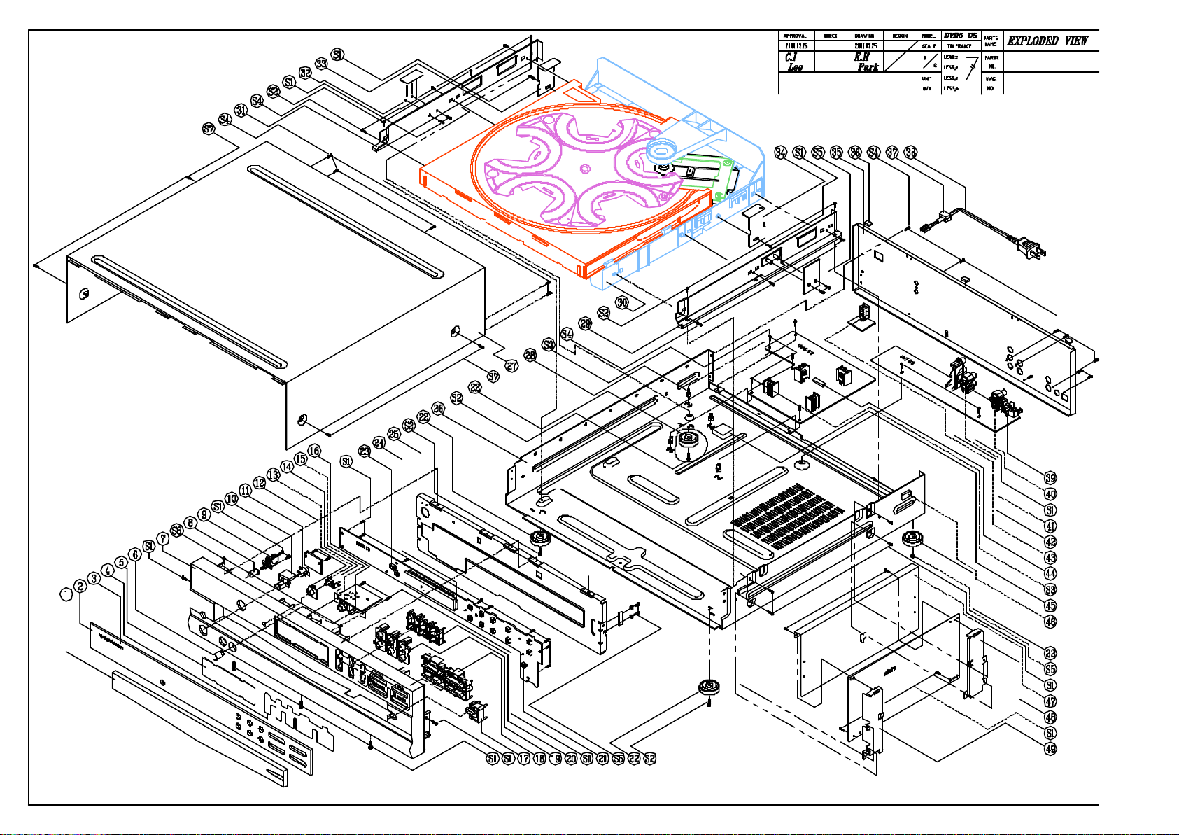
DVD5 MECHANICAL PART LIST
BADGE HARMAN/KARDO
PANEL FRONT DVD5.0
BUTTON POWER HIPS
PWR SW SDDLB14700
CORD POWER UL SPT2
CORD POWER EU 2.5A
VOLUM RK09K12A ALP
20
(A) JE990085004A MNBD ASM DVD5.0 EUR
(B) JE990089004A FRBD ASM DVD5.0 EUR
(C) JE000073001A OUTBD ASM DVD5.0 EUR
NO. PART NO. PART NAME
Q'TY
NO.
PART NO. PART NAME
Q'TY
US EU US EU
1 J85600007000 DOOR TRAY 1 1 27 J60100004000 COVER TOP 1 1
2 J85300013000 WINDOW DISPLAY 1 1 28 J85820001100 SPACER PCB 4 4
3 J60550003000
4 J85940004000 DIFFUSER DVD5.0 1 1 30 4KTDCD5D001A ASS'Y CDM5D 1 1
5 J85500005000 FILTER FL 1 1 31 J60200007000 FRAME MECHA L 1 1
6 J85100011000 KNOB LEVEL 1 1 32 J60300044000 BKT MECHA MID 1 1
7 J85000009000
8 J85200049000
9 J46203000101
10 J85200052000 BUTTON STANDBY 1 1 J60110004200 PANEL REAR - 1
11 J85400019000 INDICATOR STANDBY 1 1 36 J94100008000 SHIELD FORM 3 3
12 J85400024000 CAP BUT DIMMER 1 1 37 J65100000100 BUSHING-AC CORD 1 1
13 J85200059200 BUT DIMMER 1 1 J43730100100
14 J60300024000 BKT PHONE 1 1 J43731100000
15 J44329000102 JACK MIC 9P GOLD 1 1 39 J44301000100 JACK RCA 1P BK GND 1 1
16 J32214000401
17 J85200055000 BUT OPEN/CLOSE 1 1 41 J44312000100 JACK RCA+S GNDCAP 1 1
18 J85200059000 BUTTON PLAY 1 1 J44372100205 SCART CONNECTOR - 2
19 J85400029000 CAP BUT DISC 1 1 J44303000200 JACK RCA 3P RBG 1 20 J85200059100 BUT DISC 1 1 43 J44320000005 JACK REMOTEIH 3.5* 1 1
21 J46500500501 SW TACT SKQNAE 14 14 44 J67300013000 SPONG CUSHION 1 1
22 J85900501000 FOOT-ASS'Y 4 4 45 J97200501000 PCB SPONGE 1 1
23 J67300010000 SPONGE SENSE 1 1 46 J94100006000 SHIELD FORM 6 6
24 J67300009000 SPONGE FL 2 2 47 J60600008000 SHIELD MPEG FRONT 1 1
25 J60020002000 CHASSIS FRONT 1 1 48 J60300023100 BKT MPER REAR 1 1
26 J60000006000 CHASSIS MAIN 1 1 49 J60300023000 BKT MPEG FRONT 1 1
1 1 29 J60200007100 FRAME MECHA R 1 1
1 1 33 J60300045200 BKT MECHA LEFT 1 1
1 1 34 J60300045000 BKT MECHA RIGHT 1 1
1 1 J60110004000 PANEL REAR 1
1 1 40 J44302000600 JACK RCA 2P, JE020 1 1
35
38
42
1 -
- 1
Page 22
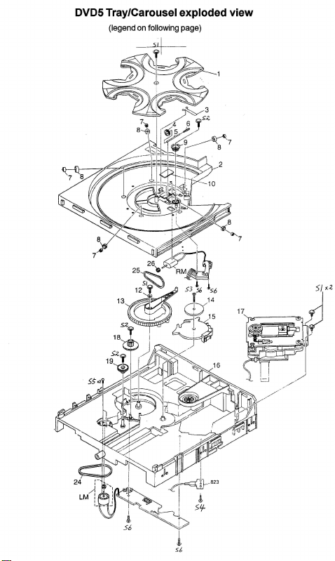
21
Page 23

Legend for DVD5 Tray/Carousel exploded view
0
22
ITEM # Part Number Description Q'ty
1 55020070XX AC PLASTIC PLASTIC CD5D 1
2 55020080XX AC PLASTIC DRAWER CD5D 1
3 20712060XX AC SPRING CLIP CD5 1
4 20711410XX AC PLASTIC PULLEY CD5 1
5 20711380XX AC METAL SHAFT CD5 1
6 20710170XX AC MLD GEAR WORM CD5 1
7 20712170XX AC PLASTIC ROLLER HUB CD5 5
8 20712120XX AC RUBBER ROLLER CD5 5
9 20710180XX AC MLD GEAR HELICAL CD5 1
10 20634190XX FELT BK 30.0MMX25.0MM 0.8MM 0MM 0 0 1
RM 20581820XX AD ASY MOTOR DC FF-130SH-14230 1
12 55190760XX WASHER-SPR 7.3MM 14.0MM 0.4MM Y 00 0 0 1
13 55020110XX AC MLD GEAR MAIN CD5D 1
14 J60300048000 WASHER 55MM 1
15 20712230XX AC PLASTIC CAM LIFTER CD5 1
16 55020090XX AC PLASTIC BASE CD5D 1
17 10665110XX DVD5 PICK-UP ASSEMBLY 1
18 20712240XX AC MLD GEAR DRIVE CD5 1
19 20712250XX AC MLD GEAR PULLEY CD5 1
LM
24 20712270XX AC RUBBER BELT DRIVE CD5 1
25 20710160XX AC RUBBER BELT PLATTER CD5 1
26 20584560XX AC RAW WHEEL BELT 1
823 J60300036000 BKT GROUND MECHA 1
20584560XX AC RAW WHEEL BELT 1
20581800XX AD ASY MOTOR DC RF-500TB 1
S1 20366370XX SCREW-SPEC 3MM 10MM JIS LARGE WASHER HD 53 0
S2 20692300XX SCREW-ST 3MM 10MM JIS B 1122 53 0 0 3
S3 J80200031820 SCREW 3*18 1
S4 55127120XX SCREW-ST 3MM 8MM JIS B 1122 53 0 0 1
S5 20349530XX SCREW 2.6MM 4MM JIS B 1111 53 0 0 2
S6 20349380XX SCREW-ST 3MM 08MM JIS B 1122 53 0 0 4
4
Page 24
23
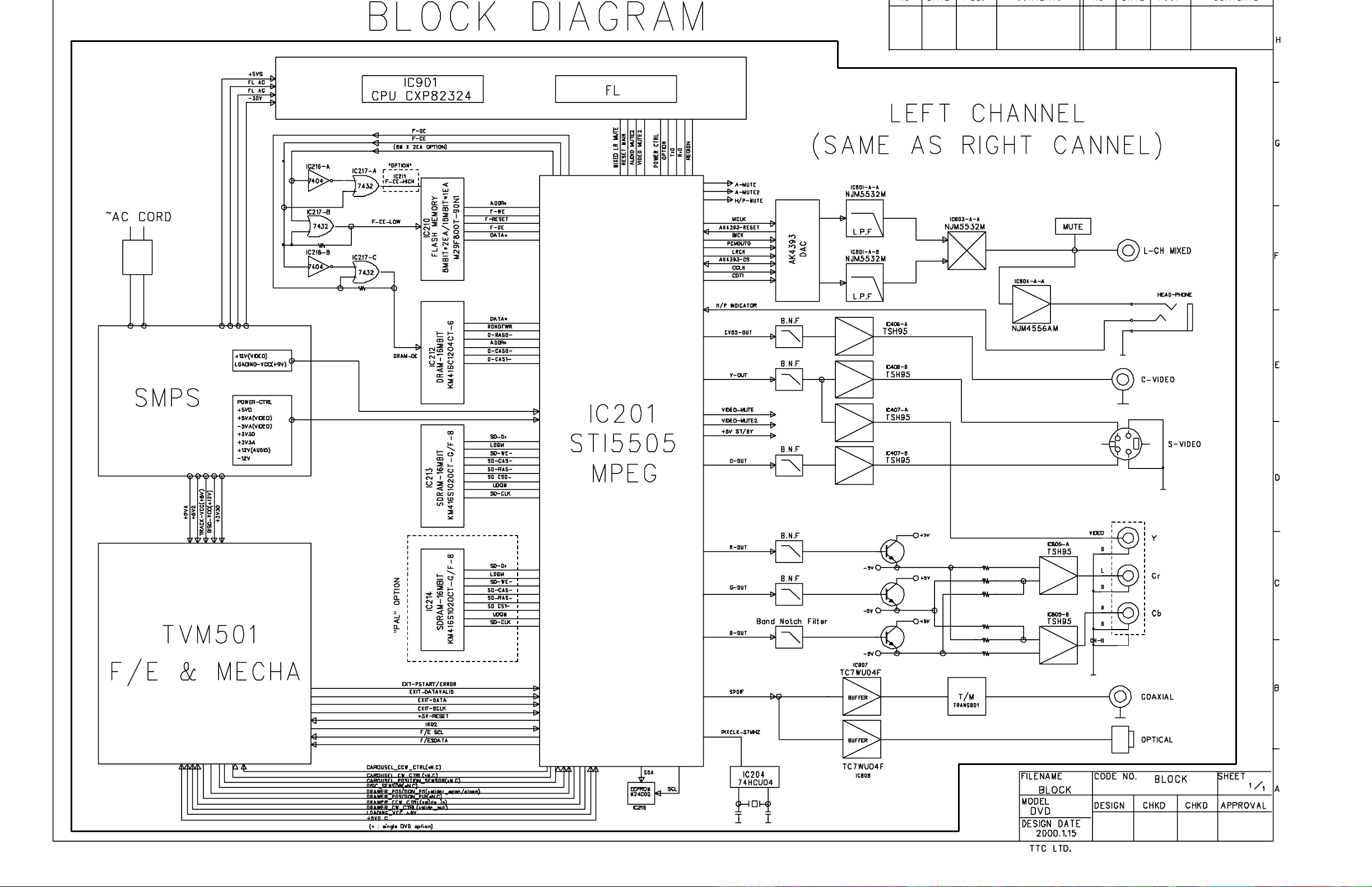
Page 25

DVD5 ELECTRICAL PARTS LIST
A-A J4141302001Y HOOK UP 90MM 1P 26 PC 1
24
DWG NO.: JE990085
TITLE : 5DVD SERIES MNBD ASM
-------------------------------------------- #001 JE990085001A MNBD ASM 5DVD PC
#002 JE990085002A MNBD ASM VC5000 PC
#003 JE990085003A MNBD ASM DAV5022 PC
#004 JE990085004A MNBD ASM DVD5.0 EU PC
'020 JE990088001A MNBD SMT 5DVD PC 1
'020 JE990088002A MNBD SMT DAV5022 PC 1
'020 JE990088003A MNBD SMT DVD5.0 EU PC 1
'090 J60600008000 SHIELD MPEG FRONT PC 1
'100 J4112103001X CARD CABLE 10P 1.2 PC 1
CC203 J4111212000X CABLE 21P 200 1.0 PC 1
CC203 J4111212200X CABLE 21P 220 1.0 PC 1
CC205 J4111152000X CABLE 15P 200 1.0 PC 1
CC207 J4112120600X CABLE 12P 60 1.25 PC 1
CC207 J4112122001X CABLE 12P 200 1.25 PC 1
CN200 J4350009914X CNT 17P SHELD 650 PC 1
CP206 J4420031240X CNT PLUG12P 2.0MM PC 1
CP212 J4420030240X CON WAFER 2P 2.0 PC 1
CP213 J4420030440X CNT PLUG 4P 2.0MM PC 1
CP214 J4420031140X CNT ST 11P 2.0 PC 1
FC101 J2632400016X FERRITE CORE 12 BO PC 1
FC102 J2632400016X FERRITE CORE 12 BO PC 1
FC103 J2632400026X FERRITE CORE 14 BO PC 1
FC104 J2632400026X FERRITE CORE 14 BO PC 1
FC105 J2632100016X EMI CORE RING34 34 PC 1
LG01 J4141300501Y HOOK-UP 50 1P #26 PC 1
LG02 J4141300901X HOOK-UP 90 1P #26 PC 1
LM201 J2612222023X COIL RA 22UH K PC 1
L206 J2612222923X 2.2UH KS0606-2R2K PC 1
X201 J3914010036X CRYSTAL 27M 16.5PF PC 1
DWG NO.: JE990089
TITLE : 5DVD SERIES FRBD ASM
---------------------------------------- #001 JE990089001A FRBD ASM DVD5.0 PC
#002 JE990089002A FRBD ASM VC5000 PC
#003 JE990089003A FRBD ASM DAV5022 PC
#004 JE990089004A FRBD ASM DVD5.0 EU PC
'020 JE990090001A FRBD APP DVD5.0 PC 1
'020 JE990090002A FRBD APP VC5000 PC 1
'020 JE990090003A FRBD APP DAV5022 PC 1
'020 JE990090004A FRBD APP DVD5.0 EU PC 1
'050 J67300009000 SPONGE FL PC 1
'070 J67300010000 SPONGE FL PC 1
'090 20932870XX AC PRI LABEL QC CH PC 1
'100 J60300021000 BKT POWER PC 1
'100 J60300024000 BKT PHONE PC 1
BK901 J5222000950X BKT GND SPTE PC 1
CC902 J4111131500X CARD 1.0 13P 150 PC 1
CN901 J4350009906X CNT 5P 240 2.0 #26 PC 1
CN902 J4422101327X FPC PLUG 1.0 13P PC 1
CN903 J4350009905X CNT 4P 140 2.0 #26 PC 1
CN903 J4350009912X CNT 2P 140 2.0 #26 PC 1
CN904 J4350009907X CNT 3P 600 2.0 #26 PC 1
CN904 J4350009910X CNT 4P 600 2.0 #26 PC 1
CN905 J4350009908X CNT 500 #18 7.92 PC 1
CP801 J4420030340X CNT PLUG 2.0 ST 3P PC 1
CP901 J4420030340X CNT PLUG 2.0 ST 3P PC 1
CP903 J4420030240X CON WAFER 2P 2.0 PC 1
CP903 J4420030440X CNT PLUG 4P 2.0MM PC 1
CP904 J4420030340X CNT PLUG 2.0 ST 3P PC 1
CP904 J4420030440X CNT PLUG 4P 2.0MM PC 1
C901 J3470947030X CE 47U 16V PC 1
C907 J3471247116X CE SR470U 6V3 M8*9 PC 1
C907 J3471347116X CE SS470U 6V3 M8*9 PC 1
C918 J3471347116X CE SS470U 6V3 M8*9 PC 1
C919 J3471247116X CE SR470U 6V3 M8*9 PC 1
C920 J3471347116X CE SS470U 6V3 M8*9 PC 1
DG901 J44302000500 2P OO JE020059 PC 1
DG901 J44320000005 JACK REMOTEIH 3.5* PC 1
D904 J2302310012X LED RED/GREEN 5 PC 1
D904 J2305211012X LED LTL-1CHGE 3RED PC 1
D907 J2221216000X DIODE RECT IN4004 PC 1
D908 J2221216000X DIODE RECT IN4004 PC 1
EC901 J2632410025X EMI CORE W5 ZP160R PC 1
FC901 J2632400015X FERRITE CORE CLAMP PC 1
FL901 J2350220010X VFD HNV-11SM07 PC 1
FL901 J2353220010X VFD HNV-11SM09 PC 1
FL901 J2353220050X VFD HNV-11SM13 SAM PC 1
HP901 J44329000102 JACK MIC 9P GOLD PC 1
IC901 J2132314020X IC CPU CXP82324 PC 1
IC901 J2132314042X IC CPU CXP82316-53 PC 1
IC901 J2132314043X IC CPU CXP82532-17 PC 1
IC902 J2112505034X IC KIA7042P 4V2 PC 1
LD901 J2301213022X LED GN LTL1CHGEC 3 PC 1
LD902 J2301213022X LED GN LTL1CHGEC 3 PC 1
LD903 J2301213022X LED GN LTL1CHGEC 3 PC 1
LD904 J2301213022X LED GN LTL1CHGEC 3 PC 1
LD905 J2301213022X LED GN LTL1CHGEC 3 PC 1
LD906 J2301213022X LED GN LTL1CHGEC 3 PC 1
LD907 J2301213022X LED GN LTL1CHGEC 3 PC 1
LD908 J2301213022X LED GN LTL1CHGEC 3 PC 1
LD909 J2301213022X LED GN LTL1CHGEC 3 PC 1
LD910 J2301213022X LED GN LTL1CHGEC 3 PC 1
LD911 J2301213022X LED GN LTL1CHGEC 3 PC 1
LD912 J2301213022X LED GN LTL1CHGEC 3 PC 1
LD913 J2301213022X LED GN LTL1CHGEC 3 PC 1
LD914 J2301213022X LED GN LTL1CHGEC 3 PC 1
LD915 J2301213022X LED GN LTL1CHGEC 3 PC 1
LD916 J2301213022X LED GN LTL1CHGEC 3 PC 1
LD917 J2301213022X LED GN LTL1CHGEC 3 PC 1
LD918 J2301213022X LED GN LTL1CHGEC 3 PC 1
OP901 J2123233001X IC LTV817 PC 1
PSW90 J46203000101 PWR SW SDDLB14700 PC 1
RM901 J2411120014X S-REMOTE 38KHZ JRC PC 1
RM901 J2411320024X REOTE RPM6938 38KH PC 1
RM901 J2411340013X RMC LTM-97AT-36N 3 PC 1
SL901 J46100000401 SW SSSF110300 PC 1
VR901 J32214000401 VOLUM RK09K12A ALP PC 1
WIRE1 J4134300701Y HOOK-UP 60MM #24BK PC 1
WIRE1 J4141302001X HOOK-UP 200 1P #26 PC 1
WIRE2 J4134300701Y HOOK-UP 60MM #24BK PC 1
WIRE2 J4134300851Y HOOK-UP 70MM #24BK PC 1
WIRE3 J4141301001X WIRE 1P 100 #24 PC 1
WIRE3 J4141301201X WIRE 120 1P #24BK PC 1
WIRE3 J4141301401X LUG 140 1P #24 BK PC 1
WIRE4 J4141301401X LUG 140 1P #24 BK PC 1
WIRE5 J4141302001Y HOOK UP 90MM 1P 26 PC 1
DWG NO.: JE990093
TITLE : 5DVD SER. OUTBD ASM
------------------------------------------ #001 JE990093001A OUTBD ASM 5DVD PC
#002 JE990093002A OUTBD ASM VC5000 PC
#003 JE990093003A OUTBD ASM DAV5022 PC
'020 JE990094001A OUTBD APP 5DVD PC 1
'020 JE990094002A OUTBD APP VC5000 PC 1
'020 JE990094003A OUTBD APP DAV5022 PC 1
CN801 J4350009913X CNT 3P 900 2.0#26 PC 1
CN802 J4350009903X CNT 10P 200 2.0 #2 PC 1
CP203 J4422002127X FPC ST 1.0 21P PC 1
CP205 J4422001527X FPC ST 1.0 15P PC 1
CP801 J4420030340X CNT PLUG 2.0 ST 3P PC 1
Page 26

F801L J3927001001X EMI FILTER TU20MT PC 1
W101 J4141301501X WIRE 1P 150MM #24 PC 1
25
F801R J3927001001X EMI FILTER TU20MT PC 1
IC806 J2123829001X FIBER OPT GP1F32T PC 1
JK803 J44303000200 JACK RCA 3P RBG PC 1
JK804 J44312000100 JACK RCA+S GNDCAP PC 1
JK806 J44302000600 JACK RCA 2P, JE020 PC 1
JK807 J44301000100 JACK RCA 1P BK GND PC 1
Q809 J2021200002X TR PNP DTA114YS PC 1
Q810L J2021060001X TR NPN KTD1302 B PC 1
Q810R J2021060001X TR NPN KTD1302 B PC 1
R883 J3003222220X RES CF 2K2 1/8W J PC 1
R884 J3003222220X RES CF 2K2 1/8W J PC 1
TS801 J2831000014X PULSE TRANS DAP-99 PC 1
TS801 J2831020105X PULSE TRANS EP-7 2 PC 1
DWG NO.: JE990153
TITLE : CDM5D MNBD ASM
---------------------------------- #001 JE990153001A CDM5D MNBD ASM PC
#002 JE990153002A CDM5E MNBD ASM PC
'020 JE990154001A CDM5D MNBD APP PC 1
CP210 J4420011206X CNT ST 1.27 PC 1
CP211 J4422111220X FPC 1.25 12P PC 1
C001 80434590AF CC 22P0F +5% -5% 5 PC 1
C002 20246950AF CC 100N0F +10% -10 PC 1
C003 80434590AF CC 22P0F +5% -5% 5 PC 1
C004 20246950AF CC 100N0F +10% -10 PC 1
C005 20268030AM CE 1MI0F +20% 25.0 PC 1
D001 2041428001 D-ZENER 1N5232B 5. PC 1
D002 2041428001 D-ZENER 1N5232B 5. PC 1
IC001 20458950NR IC-MOTORCIR BA6209 PC 1
IC001 20656300NR IC-MOTORCIR LB1641 PC 1
IC002 20458950NR IC-MOTORCIR BA6209 PC 1
IC002 20656300NR IC-MOTORCIR LB1641 PC 1
L001 20265120NR LF 39U0H +10% 130M PC 1
M021 20656240XX MAT-ING DOW CORNIN KG .
M022 20457000XX MAT-ING DOW CORNIN KG .
PI001 20586840NR D-PHOTO RPI-574 PC 1
PI001 20621240NR D-PHOTO GP1S58V 20 PC 1
PI002 20586840NR D-PHOTO RPI-574 PC 1
PI002 20621240NR D-PHOTO GP1S58V 20 PC 1
PI003 20586840NR D-PHOTO RPI-574 PC 1
PI003 20621240NR D-PHOTO GP1S58V 20 PC 1
PI004 20556130NR D-PHOTO GP2S28 20M PC 1
P003 20504010XX CONN 2.0MM 6 MA ST PC 1
P004 20713210XX WCL 150-05-05 UL24 PC 1
P027 20713500NR WCASSY 06187F 06 1 PC 1
P406 J4350009909X CNT 12P 280 #26 2 PC 1
P406B 20649240XX WCL 060-05-05 UL24 PC 1
R003 2054943001 RCFF 2R2 OHM +5% 2 PC 1
R004 2054943001 RCFF 2R2 OHM +5% 2 PC 1
0003 20712960XX AC SCHEMATIC DWG C PC 1.
DWG NO.: JE990088
TITLE : 5DVD SERIES MNBD SMT
--------------------------------- #001 JE990088001A MNBD SMT 5DVD PC
#002 JE990088002A MNBD SMT DAV5022 PC
#003 JE990088003A MNBD SMT DVD5.0 EU PC
'020 J4030100010X MN PCB 220*120 PC 1
'020 J40301000101 MN PCB 220*120 PC 1
CM207 J3470010106X CE 100UF 16V PC 1
CM208 J3515100270X CC CHIP 10PF 50V D PC 1
CM209 J3515100270X CC CHIP 10PF 50V D PC 1
CM210 J3515100270X CC CHIP 10PF 50V D PC 1
CM211 J3515100270X CC CHIP 10PF 50V D PC 1
CM212 J3515100270X CC CHIP 10PF 50V D PC 1
CM213 J3515100270X CC CHIP 10PF 50V D PC 1
CM214 J3515100270X CC CHIP 10PF 50V D PC 1
CM215 J3515100270X CC CHIP 10PF 50V D PC 1
CN203 J4422402123X FPC ST 1.0 21P PC 1
CN205 J4422401523X FPC ST 1.0 15P PC 1
CN208 J4422501327X FPC ANG 1.0 13P PC 1
CP202 J4422401523X FPC ST 1.0 15P PC 1
CP207 J4422411220X FPC ST 1.25 12P PC 1
CP802 J4425031040X CNT SMD 10P 2.0 PC 1
C206 J3515100270X CC CHIP 10PF 50V D PC 1
C211 J3525104540X CC/CHIP 0.1U 25V Z PC 1
C213 J3525104540X CC/CHIP 0.1U 25V Z PC 1
C214 J3525104540X CC/CHIP 0.1U 25V Z PC 1
C215 J3525104540X CC/CHIP 0.1U 25V Z PC 1
C216 J3470010106X CE 100UF 16V PC 1
C217 J3525103170X CC/CHIP .01U 50V K PC 1
C218 J3515331170X CC/CHIP 330PF 50V PC 1
C219 J3525332170X CC/CHIP 3300PF 50V PC 1
C220 J3525103170X CC/CHIP .01U 50V K PC 1
C221 J3470010106X CE 100UF 16V PC 1
C222 J3470010106X CE 100UF 16V PC 1
C223 J3525103170X CC/CHIP .01U 50V K PC 1
C226 J3525104540X CC/CHIP 0.1U 25V Z PC 1
C227 J3525104540X CC/CHIP 0.1U 25V Z PC 1
C228 J3525104540X CC/CHIP 0.1U 25V Z PC 1
C229 J3525104540X CC/CHIP 0.1U 25V Z PC 1
C230 J3525104540X CC/CHIP 0.1U 25V Z PC 1
C239 J3515220270X CC/CHIP 22P 50V PC 1
C239 J3515240270X CC/CHIP 24PF 50V 2 PC 1
C240 J3515220270X CC/CHIP 22P 50V PC 1
C240 J3515240270X CC/CHIP 24PF 50V 2 PC 1
C241 J3525104540X CC/CHIP 0.1U 25V Z PC 1
C242 J3525104540X CC/CHIP 0.1U 25V Z PC 1
C243 J3525104540X CC/CHIP 0.1U 25V Z PC 1
C244 J3525104540X CC/CHIP 0.1U 25V Z PC 1
C245 J3525104540X CC/CHIP 0.1U 25V Z PC 1
C246 J3525104540X CC/CHIP 0.1U 25V Z PC 1
C247 J3525104540X CC/CHIP 0.1U 25V Z PC 1
C248 J3525104540X CC/CHIP 0.1U 25V Z PC 1
C249 J3525104540X CC/CHIP 0.1U 25V Z PC 1
C250 J3525104540X CC/CHIP 0.1U 25V Z PC 1
C251 J3525103170X CC/CHIP .01U 50V K PC 1
C252 J3470010106X CE 100UF 16V PC 1
C253 J3525103170X CC/CHIP .01U 50V K PC 1
C254 J3470010106X CE 100UF 16V PC 1
C255 J3525103170X CC/CHIP .01U 50V K PC 1
C256 J3470010106X CE 100UF 16V PC 1
C257 J3525103170X CC/CHIP .01U 50V K PC 1
C258 J3470010036X CE 10U 16V M 3*5.2 PC 1
C259 J3525103170X CC/CHIP .01U 50V K PC 1
C260 J3470010106X CE 100UF 16V PC 1
C261 J3525103170X CC/CHIP .01U 50V K PC 1
C262 J3470022036X CE 22U 16V M 5*5.2 PC 1
C263 J3470022036X CE 22U 16V M 5*5.2 PC 1
C265 J3515100270X CC CHIP 10PF 50V D PC 1
C266 J3515100270X CC CHIP 10PF 50V D PC 1
C267 J3515100270X CC CHIP 10PF 50V D PC 1
C268 J3515100270X CC CHIP 10PF 50V D PC 1
C270 J3515200270X CC/CHIP 20P 50V PC 1
C301 J3515100270X CC CHIP 10PF 50V D PC 1
C312 J3515471170X C-CHIP 2012SL 470P PC 1
C332 J3525104540X CC/CHIP 0.1U 25V Z PC 1
C333 J3525104540X CC/CHIP 0.1U 25V Z PC 1
C334 J3525104540X CC/CHIP 0.1U 25V Z PC 1
C335 J3525104540X CC/CHIP 0.1U 25V Z PC 1
C336 J3470022036X CE 22U 16V M 5*5.2 PC 1
C337 J3525104540X CC/CHIP 0.1U 25V Z PC 1
C338 J3525104540X CC/CHIP 0.1U 25V Z PC 1
C348 J3470010036X CE 10U 16V M 3*5.2 PC 1
C349 J3525104540X CC/CHIP 0.1U 25V Z PC 1
C350 J3525104540X CC/CHIP 0.1U 25V Z PC 1
Page 27

C351 J3470022036X CE 22U 16V M 5*5.2 PC 1
26
C353 J3525104540X CC/CHIP 0.1U 25V Z PC 1
C354 J3525104540X CC/CHIP 0.1U 25V Z PC 1
C355 J3525104540X CC/CHIP 0.1U 25V Z PC 1
C356 J3525104540X CC/CHIP 0.1U 25V Z PC 1
C357 J3525104540X CC/CHIP 0.1U 25V Z PC 1
C358 J3525104540X CC/CHIP 0.1U 25V Z PC 1
C359 J3525104540X CC/CHIP 0.1U 25V Z PC 1
C360 J3525104540X CC/CHIP 0.1U 25V Z PC 1
C361 J3525104540X CC/CHIP 0.1U 25V Z PC 1
C362 J3525104540X CC/CHIP 0.1U 25V Z PC 1
C363 J3525104540X CC/CHIP 0.1U 25V Z PC 1
C364 J3525104540X CC/CHIP 0.1U 25V Z PC 1
C365 J3515330270X CC/CHIP 33P 50V J PC 1
C366 J3515330270X CC/CHIP 33P 50V J PC 1
C367 J3515330270X CC/CHIP 33P 50V J PC 1
C368 J3515330270X CC/CHIP 33P 50V J PC 1
C369 J3515330270X CC/CHIP 33P 50V J PC 1
C401 J3525104540X CC/CHIP 0.1U 25V Z PC 1
C402 J3470022116X CE 220U 6.3V M 6.3 PC 1
C403 J3525104540X CC/CHIP 0.1U 25V Z PC 1
C404 J3470022116X CE 220U 6.3V M 6.3 PC 1
C405 J3525104540X CC/CHIP 0.1U 25V Z PC 1
C406 J3470022116X CE 220U 6.3V M 6.3 PC 1
C408 J3470022116X CE 220U 6.3V M 6.3 PC 1
C409 J3525104540X CC/CHIP 0.1U 25V Z PC 1
C410 J3515200270X CC/CHIP 20P 50V PC 1
C411 J3515680270X CC/CHIP 68P 2012 PC 1
C412 J3515200270X CC/CHIP 20P 50V PC 1
C413 J3525104540X CC/CHIP 0.1U 25V Z PC 1
C414 J3515150270X CC/CHIP 15P 50V PC 1
C415 J3515200270X CC/CHIP 20P 50V PC 1
C416 J3515680270X CC/CHIP 68P 2012 PC 1
C417 J3515200270X CC/CHIP 20P 50V PC 1
C418 J3515150270X CC/CHIP 15P 50V PC 1
C419 J3515200270X CC/CHIP 20P 50V PC 1
C420 J3515680270X CC/CHIP 68P 2012 PC 1
C421 J3515200270X CC/CHIP 20P 50V PC 1
C422 J3515150270X CC/CHIP 15P 50V PC 1
C423 J3515200270X CC/CHIP 20P 50V PC 1
C424 J3515680270X CC/CHIP 68P 2012 PC 1
C425 J3515200270X CC/CHIP 20P 50V PC 1
C426 J3515150270X CC/CHIP 15P 50V PC 1
C427 J3515200270X CC/CHIP 20P 50V PC 1
C428 J3515680270X CC/CHIP 68P 2012 PC 1
C429 J3515200270X CC/CHIP 20P 50V PC 1
C430 J3515150270X CC/CHIP 15P 50V PC 1
C431 J3515200270X CC/CHIP 20P 50V PC 1
C432 J3515680270X CC/CHIP 68P 2012 PC 1
C433 J3515200270X CC/CHIP 20P 50V PC 1
C434 J3515150270X CC/CHIP 15P 50V PC 1
C435 J3525104540X CC/CHIP 0.1U 25V Z PC 1
C436 J3525104540X CC/CHIP 0.1U 25V Z PC 1
C440 J3470010106X CE 100UF 16V PC 1
C441 J3525104540X CC/CHIP 0.1U 25V Z PC 1
C450 J3470010036X CE 10U 16V M 3*5.2 PC 1
C451 J3525104540X CC/CHIP 0.1U 25V Z PC 1
C452 J3525104540X CC/CHIP 0.1U 25V Z PC 1
C453 J3470010036X CE 10U 16V M 3*5.2 PC 1
C454 J3525104540X CC/CHIP 0.1U 25V Z PC 1
C455 J3470010036X CE 10U 16V M 3*5.2 PC 1
C460 J3470010036X CE 10U 16V M 3*5.2 PC 1
C461 J3525104540X CC/CHIP 0.1U 25V Z PC 1
C486 J3470033116X CE 330U 6.3V M 8*6 PC 1
C487 J3525104540X CC/CHIP 0.1U 25V Z PC 1
C488 J3525104540X CC/CHIP 0.1U 25V Z PC 1
C489 J3525104540X CC/CHIP 0.1U 25V Z PC 1
C490 J3525104540X CC/CHIP 0.1U 25V Z PC 1
C495 J3470033116X CE 330U 6.3V M 8*6 PC 1
C496 J3525104540X CC/CHIP 0.1U 25V Z PC 1
C497 J3525104540X CC/CHIP 0.1U 25V Z PC 1
C498 J3525104540X CC/CHIP 0.1U 25V Z PC 1
C499 J3525104540X CC/CHIP 0.1U 25V Z PC 1
C503 J3515150270X CC/CHIP 15P 50V PC 1
C504 J3515150270X CC/CHIP 15P 50V PC 1
C505 J3525104540X CC/CHIP 0.1U 25V Z PC 1
C506 J3525104540X CC/CHIP 0.1U 25V Z PC 1
C507 J3515100270X CC CHIP 10PF 50V D PC 1
C508 J3515100270X CC CHIP 10PF 50V D PC 1
C509 J3515100270X CC CHIP 10PF 50V D PC 1
C510 J3515100270X CC CHIP 10PF 50V D PC 1
C511 J3515100270X CC CHIP 10PF 50V D PC 1
C512 J3515100270X CC CHIP 10PF 50V D PC 1
C513 J3515100270X CC CHIP 10PF 50V D PC 1
C520 J3470010106X CE 100UF 16V PC 1
C521 J3470010106X CE 100UF 16V PC 1
D401 J2244010104X DIODE CHIP 1SS355 PC 1
IC201 J2135307001X IC STI5505AVB PC 1
IC204 J2116007001X IC 74HCU04M1R HEX PC 1
IC211 J2131007002X IC FLASH M29F800T PC 1
IC211 J2131016001X IC FLASH TMS29LF80 PC 1
IC211 J2131041001X ICFLASH SST39VF800 PC 1
IC212 J2131003009X IC K4E151611C-TC60 PC 1
IC213 J2131003008X IC SDRAM KM4161S11 PC 1
IC213 J2131003010X IC SDRAM KS161622D PC 1
IC214 J2131003008X IC SDRAM KM4161S11 PC 1
IC215 J2131007001X IC M24C02 SOP8 PC 1
IC402 J2133031001X IC AK4393 AUDIO PC 1
IC406 J2110007001X IC TSH95D VIDEO PC 1
IC407 J2110007001X IC TSH95D VIDEO PC 1
IC408 J2112912001X IC 7805DLA REG PC 1
J201 J3024000120X RES 0 OHM 1/10W J PC 1
J202 J3024000120X RES 0 OHM 1/10W J PC 1
J203 J3024000120X RES 0 OHM 1/10W J PC 1
J204 J3024102120X RES CHIP 1K 1/10W PC 1
J205 J3024102120X RES CHIP 1K 1/10W PC 1
J206 J3024102120X RES CHIP 1K 1/10W PC 1
J207 J3024102120X RES CHIP 1K 1/10W PC 1
L202 J2611022011X COIL CHIP ELJFC220 PC 1
L203 J2611022011X COIL CHIP ELJFC220 PC 1
L205 J2631300011X BEAD 120XOHM PC 1
L207 J2631330085X BEAD FCM3216V 2K PC 1
L208 J2631330085X BEAD FCM3216V 2K PC 1
L209 J2631330085X BEAD FCM3216V 2K PC 1
L210 J2631330085X BEAD FCM3216V 2K PC 1
L211 J2631330085X BEAD FCM3216V 2K PC 1
L212 J2631330085X BEAD FCM3216V 2K PC 1
L330 J2611022011X COIL CHIP ELJFC220 PC 1
L332 J2611022011X COIL CHIP ELJFC220 PC 1
L333 J2611022011X COIL CHIP ELJFC220 PC 1
L334 J2631330085X BEAD FCM3216V 2K PC 1
L335 J2631330085X BEAD FCM3216V 2K PC 1
L336 J2631330085X BEAD FCM3216V 2K PC 1
L337 J3927201111X EMI FILTER STC104B PC 1
L338 J3927201111X EMI FILTER STC104B PC 1
L339 J2631330085X BEAD FCM3216V 2K PC 1
L340 J2631330085X BEAD FCM3216V 2K PC 1
L341 J2631330085X BEAD FCM3216V 2K PC 1
L342 J2631330085X BEAD FCM3216V 2K PC 1
L343 J2631330085X BEAD FCM3216V 2K PC 1
L344 J2631330085X BEAD FCM3216V 2K PC 1
L400 J2611022011X COIL CHIP ELJFC220 PC 1
L401 J2611022011X COIL CHIP ELJFC220 PC 1
L402 J2611022011X COIL CHIP ELJFC220 PC 1
L403 J2611022011X COIL CHIP ELJFC220 PC 1
L404 J2611082921X COIL CHIP 8.2UH PC 1
L405 J2611082921X COIL CHIP 8.2UH PC 1
L406 J2611082921X COIL CHIP 8.2UH PC 1
L407 J2611082921X COIL CHIP 8.2UH PC 1
L408 J2611082921X COIL CHIP 8.2UH PC 1
Page 28

L409 J2611082921X COIL CHIP 8.2UH PC 1
27
L410 J2611082921X COIL CHIP 8.2UH PC 1
L411 J2611082921X COIL CHIP 8.2UH PC 1
L412 J2611082921X COIL CHIP 8.2UH PC 1
L413 J2611082921X COIL CHIP 8.2UH PC 1
L414 J2611082921X COIL CHIP 8.2UH PC 1
L415 J2611082921X COIL CHIP 8.2UH PC 1
L416 J2631300011X BEAD 120XOHM PC 1
L417 J2631300011X BEAD 120XOHM PC 1
L418 J2631300011X BEAD 120XOHM PC 1
L419 J2631300011X BEAD 120XOHM PC 1
L420 J2611022011X COIL CHIP ELJFC220 PC 1
L421 J2611022011X COIL CHIP ELJFC220 PC 1
L422 J2631330085X BEAD FCM3216V 2K PC 1
L423 J3927201111X EMI FILTER STC104B PC 1
L450 J2631300011X BEAD 120XOHM PC 1
L452 J2631300011X BEAD 120XOHM PC 1
Q201 J2041020201X TR KTC3875S SOT23 PC 1
Q202 J2041020201X TR KTC3875S SOT23 PC 1
Q204 J2041020201X TR KTC3875S SOT23 PC 1
Q205 J2041020201X TR KTC3875S SOT23 PC 1
Q206 J2041020201X TR KTC3875S SOT23 PC 1
Q207 J2041220102X TR NPN DTC114YKA PC 1
Q208 J2041220102X TR NPN DTC114YKA PC 1
RA201 J3029470120X RES CHIP 47R 2010 PC 1
RA202 J3029470120X RES CHIP 47R 2010 PC 1
RA203 J3029470120X RES CHIP 47R 2010 PC 1
RA204 J3029470120X RES CHIP 47R 2010 PC 1
RA205 J3029470120X RES CHIP 47R 2010 PC 1
RA206 J3029470120X RES CHIP 47R 2010 PC 1
RA207 J3029470120X RES CHIP 47R 2010 PC 1
RA208 J3029470120X RES CHIP 47R 2010 PC 1
RA209 J3029470120X RES CHIP 47R 2010 PC 1
RA210 J3029470120X RES CHIP 47R 2010 PC 1
RA211 J3029470120X RES CHIP 47R 2010 PC 1
RA212 J3029470120X RES CHIP 47R 2010 PC 1
RA213 J3029470120X RES CHIP 47R 2010 PC 1
RA214 J3029470120X RES CHIP 47R 2010 PC 1
RA215 J3029470120X RES CHIP 47R 2010 PC 1
RA216 J3029470120X RES CHIP 47R 2010 PC 1
RM201 J3024221120X R-CHIP 220 2012J PC 1
RM202 J3024221120X R-CHIP 220 2012J PC 1
RM216 J3024103120X RES CHIP 10K 1/10W PC 1
RM217 J3024103120X RES CHIP 10K 1/10W PC 1
RM218 J3024473120X RES CHIP 47K 1/10W PC 1
RM219 J3024473120X RES CHIP 47K 1/10W PC 1
RM220 J3024473120X RES CHIP 47K 1/10W PC 1
RM221 J3024473120X RES CHIP 47K 1/10W PC 1
RM222 J3024103120X RES CHIP 10K 1/10W PC 1
RM223 J2631320105X FCM2012H-102T04 PC 1
RM224 J2631320105X FCM2012H-102T04 PC 1
RM225 J2631320105X FCM2012H-102T04 PC 1
RM226 J2631320105X FCM2012H-102T04 PC 1
RM227 J2631320105X FCM2012H-102T04 PC 1
RM228 J2631320105X FCM2012H-102T04 PC 1
RM229 J2631320105X FCM2012H-102T04 PC 1
RM230 J2631320105X FCM2012H-102T04 PC 1
RM232 J3024103120X RES CHIP 10K 1/10W PC 1
RX06 J3024000120X RES 0 OHM 1/10W J PC 1
RX08 J3024103120X RES CHIP 10K 1/10W PC 1
R201 J3024182120X RES CHIP 1K8 1/10W PC 1
R202 J3024182120X RES CHIP 1K8 1/10W PC 1
R203 J3024103120X RES CHIP 10K 1/10W PC 1
R205 J3024103120X RES CHIP 10K 1/10W PC 1
R206 J3024103120X RES CHIP 10K 1/10W PC 1
R207 J3024103120X RES CHIP 10K 1/10W PC 1
R208 J3024103120X RES CHIP 10K 1/10W PC 1
R209 J3024103120X RES CHIP 10K 1/10W PC 1
R210 J3024472120X RES CHIP 4K7 1/10W PC 1
R211 J3024472120X RES CHIP 4K7 1/10W PC 1
R212 J3024103120X RES CHIP 10K 1/10W PC 1
R213 J3024560120X RES CHIP 56 1/10WJ PC 1
R214 J3024000120X RES 0 OHM 1/10W J PC 1
R216 J3024103120X RES CHIP 10K 1/10W PC 1
R218 J30241873175 RES 18K7 1/10 1% PC 1
R219 J30241153175 RES 11K5 1/10 1% PC 1
R222 J3024000120X RES 0 OHM 1/10W J PC 1
R223 J3024000120X RES 0 OHM 1/10W J PC 1
R224 J2631320095X BEAD FCM2012V-601 PC 1
R228 J3024331120X R-CHIP 330 2012J PC 1
R229 J3024105120X RES CHIP 1M 1/10WJ PC 1
R230 J3024103120X RES CHIP 10K 1/10W PC 1
R231 J3024103120X RES CHIP 10K 1/10W PC 1
R232 J3024103120X RES CHIP 10K 1/10W PC 1
R233 J3024103120X RES CHIP 10K 1/10W PC 1
R234 J2631320065X FCM2012V-221T07 PC 1
R235 J3024470120X RES CHIP 47 1/10W PC 1
R236 J3024470120X RES CHIP 47 1/10W PC 1
R237 J3024470120X RES CHIP 47 1/10W PC 1
R238 J2631320065X FCM2012V-221T07 PC 1
R239 J2631320065X FCM2012V-221T07 PC 1
R240 J3024470120X RES CHIP 47 1/10W PC 1
R243 J2631320245X BEAD FCM2012C-121T PC 1
R244 J3024000120X RES 0 OHM 1/10W J PC 1
R247 J3024000120X RES 0 OHM 1/10W J PC 1
R248 J3024000120X RES 0 OHM 1/10W J PC 1
R249 J3024472120X RES CHIP 4K7 1/10W PC 1
R250 J3024472120X RES CHIP 4K7 1/10W PC 1
R269 J3024101120X RES CHIP 100 1/10W PC 1
R270 J3024101120X RES CHIP 100 1/10W PC 1
R271 J2631320075X FCM2012V-301T07 PC 1
R272 J2631320075X FCM2012V-301T07 PC 1
R277 J3024103120X RES CHIP 10K 1/10W PC 1
R278 J3024103120X RES CHIP 10K 1/10W PC 1
R279 J3024103120X RES CHIP 10K 1/10W PC 1
R280 J3024103120X RES CHIP 10K 1/10W PC 1
R281 J3024103120X RES CHIP 10K 1/10W PC 1
R283 J3024472120X RES CHIP 4K7 1/10W PC 1
R286 J3024470120X RES CHIP 47 1/10W PC 1
R289 J2631320105X FCM2012H-102T04 PC 1
R301 J3024000120X RES 0 OHM 1/10W J PC 1
R301 J3024122120X RES CHIP 1K2 1/10W PC 1
R330 J2631330085X BEAD FCM3216V 2K PC 1
R332 J2631330085X BEAD FCM3216V 2K PC 1
R333 J2631320125X FCM2012H-202T02 PC 1
R334 J2631320125X FCM2012H-202T02 PC 1
R335 J2631320015X FCM2012K-202T02 PC 1
R345 J3024000120X RES 0 OHM 1/10W J PC 1
R346 J3024000120X RES 0 OHM 1/10W J PC 1
R347 J3024473120X RES CHIP 47K 1/10W PC 1
R348 J3024473120X RES CHIP 47K 1/10W PC 1
R349 J2631320065X FCM2012V-221T07 PC 1
R350 J3024470120X RES CHIP 47 1/10W PC 1
R351 J2631320065X FCM2012V-221T07 PC 1
R352 J3024470120X RES CHIP 47 1/10W PC 1
R353 J3024470120X RES CHIP 47 1/10W PC 1
R354 J3024470120X RES CHIP 47 1/10W PC 1
R355 J3024470120X RES CHIP 47 1/10W PC 1
R356 J3024470120X RES CHIP 47 1/10W PC 1
R357 J3024473120X RES CHIP 47K 1/10W PC 1
R358 J3024473120X RES CHIP 47K 1/10W PC 1
R359 J3024473120X RES CHIP 47K 1/10W PC 1
R360 J3024473120X RES CHIP 47K 1/10W PC 1
R361 J3024473120X RES CHIP 47K 1/10W PC 1
R362 J3024473120X RES CHIP 47K 1/10W PC 1
R363 J3024473120X RES CHIP 47K 1/10W PC 1
R366 J3024472120X RES CHIP 4K7 1/10W PC 1
R367 J3024472120X RES CHIP 4K7 1/10W PC 1
R368 J3024472120X RES CHIP 4K7 1/10W PC 1
R369 J3024472120X RES CHIP 4K7 1/10W PC 1
Page 29

R370 J3024472120X RES CHIP 4K7 1/10W PC 1
28
R400 J3024479120X R-CHIP 4R7 2012J PC 1
R401 J3024479120X R-CHIP 4R7 2012J PC 1
R402 J3024479120X R-CHIP 4R7 2012J PC 1
R403 J3024479120X R-CHIP 4R7 2012J PC 1
R404 J3024391120X R-CHIP 390 2012J PC 1
R405 J3024391120X R-CHIP 390 2012J PC 1
R406 J3024391120X R-CHIP 390 2012J PC 1
R407 J3024681120X RES CHIP 680 1/10W PC 1
R408 J3024391120X R-CHIP 390 2012J PC 1
R409 J3024391120X R-CHIP 390 2012J PC 1
R410 J3024681120X RES CHIP 680 1/10W PC 1
R411 J3024391120X R-CHIP 390 2012J PC 1
R412 J3024391120X R-CHIP 390 2012J PC 1
R413 J3024391120X R-CHIP 390 2012J PC 1
R414 J3024471120X RES CHIP 470 1/10W PC 1
R414 J3024511120X RES CHIP 510 1/10W PC 1
R415 J3024221120X R-CHIP 220 2012J PC 1
R415 J3024271120X R-CHIP 270 1/10W J PC 1
R416 J3024391120X R-CHIP 390 2012J PC 1
R417 J3024391120X R-CHIP 390 2012J PC 1
R418 J3024391120X R-CHIP 390 2012J PC 1
R419 J3024681120X RES CHIP 680 1/10W PC 1
R420 J3024391120X R-CHIP 390 2012J PC 1
R421 J3024391120X R-CHIP 390 2012J PC 1
R422 J3024391120X R-CHIP 390 2012J PC 1
R423 J3024221120X R-CHIP 220 2012J PC 1
R424 J3024391120X R-CHIP 390 2012J PC 1
R425 J3024391120X R-CHIP 390 2012J PC 1
R426 J3024391120X R-CHIP 390 2012J PC 1
R427 J3024681120X RES CHIP 680 1/10W PC 1
R428 J3024479120X R-CHIP 4R7 2012J PC 1
R429 J3024479120X R-CHIP 4R7 2012J PC 1
R430 J3024479120X R-CHIP 4R7 2012J PC 1
R431 J3024479120X R-CHIP 4R7 2012J PC 1
R440 J3024000120X RES 0 OHM 1/10W J PC 1
R450 J3024473120X RES CHIP 47K 1/10W PC 1
R451 J3024473120X RES CHIP 47K 1/10W PC 1
R452 J3024473120X RES CHIP 47K 1/10W PC 1
R453 J3024473120X RES CHIP 47K 1/10W PC 1
R458 J3024473120X RES CHIP 47K 1/10W PC 1
R459 J3024473120X RES CHIP 47K 1/10W PC 1
R460 J3024473120X RES CHIP 47K 1/10W PC 1
R461 J3024000120X RES 0 OHM 1/10W J PC 1
R463 J3024000120X RES 0 OHM 1/10W J PC 1
R465 J3024000120X RES 0 OHM 1/10W J PC 1
R473 J3024391120X R-CHIP 390 2012J PC 1
R474 J3024681120X RES CHIP 680 1/10W PC 1
R475 J3024391120X R-CHIP 390 2012J PC 1
R476 J3024681120X RES CHIP 680 1/10W PC 1
R477 J3024391120X R-CHIP 390 2012J PC 1
R478 J3024391120X R-CHIP 390 2012J PC 1
R479 J3024391120X R-CHIP 390 2012J PC 1
R480 J3024104120X RES CHIP 100K 1/10 PC 1
R481 J3024102120X RES CHIP 1K 1/10W PC 1
R484 J3024470120X RES CHIP 47 1/10W PC 1
R485 J3024470120X RES CHIP 47 1/10W PC 1
R486 J3024470120X RES CHIP 47 1/10W PC 1
R487 J3024470120X RES CHIP 47 1/10W PC 1
R488 J3024470120X RES CHIP 47 1/10W PC 1
R489 J3024470120X RES CHIP 47 1/10W PC 1
R490 J3024470120X RES CHIP 47 1/10W PC 1
R492 J3024102120X RES CHIP 1K 1/10W PC 1
R493 J3024104120X RES CHIP 100K 1/10 PC 1
DWG NO.: JE990090
TITLE : 5DVD SERIES FRBD APP
--------------------------------------- #001 JE990090001A FRBD APP DVD5.0 PC
#002 JE990090002A FRBD APP VC5000 PC
#003 JE990090003A FRBD APP DAV5022 PC
#004 JE990090004A FRBD APP DVD5.0 EU PC
'020 JE990092001A FRBD SMT DVD5.0 PC 1
'020 JE990092002A FRBD SMT VC5000 PC 1
'020 JE990092003A FRBD SMT DAV5022 PC 1
'021 J4030100070X FR PCB 425*197(1/4 PC 1
'021 J4032100010X FR PCB 330*247 PC 1
'021 J4035100010X FR PCB 400*247 PC 1
C901 J3470947030X CE 47U 16V PC 1
C906 J3470910110X CE 100UF 6.3V PC 1
C909 J3470910970X CE 1U 50V M SS 5*7 PC 1
C912 J3513561170X CC/DISC SL 560P50V PC 1
C913 J3513561170X CC/DISC SL 560P50V PC 1
C914 J3523104540X CAP C/D/T .1U 25V PC 1
C915 J3470947030X CE 47U 16V PC 1
C916 J3471347116X CE SS470U 6V3 M8*9 PC 1
C917 J3470110211X CE 1000UF 6.3V PC 1
IC902 J2112505034X IC KIA7042P 4V2 PC 1
Q907 J2021000601X TR PNP MPSA56 Y PC 1
Q908 J2021000601X TR PNP MPSA56 Y PC 1
Q909 J2021000601X TR PNP MPSA56 Y PC 1
Q914 J2021200501X TR PNP KRA107M PC 1
SW901 J46500500002 SW TACT PC 1
SW901 J46500500501 SW TACT SKQNAE PC 1
SW902 J46500500501 SW TACT SKQNAE PC 1
SW903 J46500500002 SW TACT PC 1
SW903 J46500500501 SW TACT SKQNAE PC 1
SW904 J46500500501 SW TACT SKQNAE PC 1
SW905 J46500500002 SW TACT PC 1
SW905 J46500500501 SW TACT SKQNAE PC 1
SW906 J46500500501 SW TACT SKQNAE PC 1
SW907 J46500500002 SW TACT PC 1
SW907 J46500500501 SW TACT SKQNAE PC 1
SW909 J46500500002 SW TACT PC 1
SW909 J46500500501 SW TACT SKQNAE PC 1
SW911 J46500500002 SW TACT PC 1
SW911 J46500500501 SW TACT SKQNAE PC 1
SW912 J46500500501 SW TACT SKQNAE PC 1
SW913 J46500500002 SW TACT PC 1
SW913 J46500500501 SW TACT SKQNAE PC 1
SW914 J46500500501 SW TACT SKQNAE PC 1
SW915 J46500500002 SW TACT PC 1
SW915 J46500500501 SW TACT SKQNAE PC 1
SW916 J46500500501 SW TACT SKQNAE PC 1
SW917 J46500500002 SW TACT PC 1
SW917 J46500500501 SW TACT SKQNAE PC 1
SW919 J46500500002 SW TACT PC 1
SW919 J46500500501 SW TACT SKQNAE PC 1
SW921 J46500500002 SW TACT PC 1
SW921 J46500500501 SW TACT SKQNAE PC 1
SW924 J46500500002 SW TACT PC 1
SW924 J46500500501 SW TACT SKQNAE PC 1
SW927 J46500500002 SW TACT PC 1
SW927 J46500500501 SW TACT SKQNAE PC 1
SW930 J46500500002 SW TACT PC 1
SW930 J46500500501 SW TACT SKQNAE PC 1
SW931 J46500500002 SW TACT PC 1
SW931 J46500500501 SW TACT SKQNAE PC 1
DWG NO.: JE990092
TITLE : 5DVD SERIES FRBD SMT
--------------------------------------- #001 JE990092001A FRBD SMT DVD5.0 PC
#002 JE990092002A FRBD SMT VC5000 PC
#003 JE990092003A FRBD SMT DAV5022 PC
C903 J3525104540X CC/CHIP 0.1U 25V Z PC 1
C904 J3525104540X CC/CHIP 0.1U 25V Z PC 1
C905 J3525104540X CC/CHIP 0.1U 25V Z PC 1
Page 30

C908 J3525104540X CC/CHIP 0.1U 25V Z PC 1
29
C911 J3525104540X CC/CHIP 0.1U 25V Z PC 1
C916 J3525104540X CC/CHIP 0.1U 25V Z PC 1
D906 J2242510011X D SCHOTTKY RB501V- PC 1
D906 J2244010104X DIODE CHIP 1SS355 PC 1
D907 J2242510011X D SCHOTTKY RB501V- PC 1
D908 J2242251011X D-CHIP RB501V-40 U PC 1
J941 J3024000120X RES 0 OHM 1/10W J PC 1
J942 J3024000120X RES 0 OHM 1/10W J PC 1
J943 J3024000120X RES 0 OHM 1/10W J PC 1
J944 J3024000120X RES 0 OHM 1/10W J PC 1
L901 J2611022011X COIL CHIP ELJFC220 PC 1
L902 J2631330085X BEAD FCM3216V 2K PC 1
L903 J2631330085X BEAD FCM3216V 2K PC 1
L904 J2631330085X BEAD FCM3216V 2K PC 1
L905 J3927201111X EMI FILTER STC104B PC 1
L906 J3927201111X EMI FILTER STC104B PC 1
L908 J2631330085X BEAD FCM3216V 2K PC 1
L909 J2631330085X BEAD FCM3216V 2K PC 1
L912 J2631330085X BEAD FCM3216V 2K PC 1
L913 J2631330085X BEAD FCM3216V 2K PC 1
L914 J2631330085X BEAD FCM3216V 2K PC 1
L915 J2631330085X BEAD FCM3216V 2K PC 1
Q902 J2041220102X TR NPN DTC114YKA PC 1
Q904 J2041220102X TR NPN DTC114YKA PC 1
Q906 J2041220102X TR NPN DTC114YKA PC 1
Q913 J2041220102X TR NPN DTC114YKA PC 1
Q914 J2041200102X TR PNP DTA114YKA PC 1
Q915 J2041220102X TR NPN DTC114YKA PC 1
R901 J3024101120X RES CHIP 100 1/10W PC 1
R902 J3024103120X RES CHIP 10K 1/10W PC 1
R909 J3024221120X R-CHIP 220 2012J PC 1
R910 J3024181120X RES CHIP 180 1/10W PC 1
R910 J3024681120X RES CHIP 680 1/10W PC 1
R911 J3024182120X RES CHIP 1K8 1/10W PC 1
R911 J3024242120X RES CHIP 2K4 1/10 PC 1
R911 J3024332120X RES CHIP 3K3 1/10W PC 1
R912 J3024332120X RES CHIP 3K3 1/10W PC 1
R912 J3024682120X RES CHIP 6K8 1/10W PC 1
R913 J3024203120X RES CHIP 20K 1/10W PC 1
R913 J3024472120X RES CHIP 4K7 1/10W PC 1
R913 J3024822120X R-CHIP 8K2 1/10W J PC 1
R914 J3024103120X RES CHIP 10K 1/10W PC 1
R914 J3024333120X RES CHIP 33K 1/10W PC 1
R915 J3024333120X RES CHIP 33K 1/10W PC 1
R916 J3024184120X R-CHIP 180K 2012J PC 1
R921 J3024182120X RES CHIP 1K8 1/10W PC 1
R921 J3024242120X RES CHIP 2K4 1/10 PC 1
R921 J3024332120X RES CHIP 3K3 1/10W PC 1
R922 J3024332120X RES CHIP 3K3 1/10W PC 1
R922 J3024682120X RES CHIP 6K8 1/10W PC 1
R923 J3024203120X RES CHIP 20K 1/10W PC 1
R923 J3024472120X RES CHIP 4K7 1/10W PC 1
R923 J3024822120X R-CHIP 8K2 1/10W J PC 1
R924 J3024103120X RES CHIP 10K 1/10W PC 1
R924 J3024333120X RES CHIP 33K 1/10W PC 1
R925 J3024333120X RES CHIP 33K 1/10W PC 1
R926 J3024223120X RES CHIP 22K 1/10W PC 1
R926 J3024473120X RES CHIP 47K 1/10W PC 1
R927 J3024223120X RES CHIP 22K 1/10W PC 1
R927 J3024473120X RES CHIP 47K 1/10W PC 1
R931 J3024242120X RES CHIP 2K4 1/10 PC 1
R931 J3024332120X RES CHIP 3K3 1/10W PC 1
R932 J3024682120X RES CHIP 6K8 1/10W PC 1
R933 J3024203120X RES CHIP 20K 1/10W PC 1
R933 J3024822120X R-CHIP 8K2 1/10W J PC 1
R934 J3024333120X RES CHIP 33K 1/10W PC 1
R938 J3024103120X RES CHIP 10K 1/10W PC 1
R939 J3024103120X RES CHIP 10K 1/10W PC 1
R940 J3024103120X RES CHIP 10K 1/10W PC 1
R941 J3024103120X RES CHIP 10K 1/10W PC 1
R942 J3024103120X RES CHIP 10K 1/10W PC 1
R943 J3024473120X RES CHIP 47K 1/10W PC 1
R944 J3024103120X RES CHIP 10K 1/10W PC 1
R945 J3024000120X RES 0 OHM 1/10W J PC 1
R945 J3024122120X RES CHIP 1K2 1/10W PC 1
R946 J3024221120X R-CHIP 220 2012J PC 1
R947 J3024681120X RES CHIP 680 1/10W PC 1
R948 J3024103120X RES CHIP 10K 1/10W PC 1
R949 J3024822120X R-CHIP 8K2 1/10W J PC 1
R951 J3024181120X RES CHIP 180 1/10W PC 1
R952 J3024181120X RES CHIP 180 1/10W PC 1
R953 J3024181120X RES CHIP 180 1/10W PC 1
R954 J3024181120X RES CHIP 180 1/10W PC 1
R955 J3024181120X RES CHIP 180 1/10W PC 1
R956 J3024181120X RES CHIP 180 1/10W PC 1
R957 J3024181120X RES CHIP 180 1/10W PC 1
R958 J3024181120X RES CHIP 180 1/10W PC 1
R959 J3024181120X RES CHIP 180 1/10W PC 1
R960 J3024181120X RES CHIP 180 1/10W PC 1
R961 J3024101120X RES CHIP 100 1/10W PC 1
R961 J3024181120X RES CHIP 180 1/10W PC 1
R962 J3024181120X RES CHIP 180 1/10W PC 1
R963 J3024181120X RES CHIP 180 1/10W PC 1
R964 J3024103120X RES CHIP 10K 1/10W PC 1
R964 J3024181120X RES CHIP 180 1/10W PC 1
R965 J3024181120X RES CHIP 180 1/10W PC 1
R965 J3024473120X RES CHIP 47K 1/10W PC 1
R966 J3024181120X RES CHIP 180 1/10W PC 1
R967 J3024181120X RES CHIP 180 1/10W PC 1
R968 J3024181120X RES CHIP 180 1/10W PC 1
R968 J3024220120X RES CHIP 22 1/10W PC 1
R970 J3024102120X RES CHIP 1K 1/10W PC 1
R972 J3024102120X RES CHIP 1K 1/10W PC 1
R973 J3024102120X RES CHIP 1K 1/10W PC 1
R974 J3024332120X RES CHIP 3K3 1/10W PC 1
R975 J3024332120X RES CHIP 3K3 1/10W PC 1
R976 J3024332120X RES CHIP 3K3 1/10W PC 1
R983 J2244010104X DIODE CHIP 1SS355 PC 1
R984 J3024271120X R-CHIP 270 1/10W J PC 1
R985 J3024103120X RES CHIP 10K 1/10W PC 1
R986 J3024391120X R-CHIP 390 2012J PC 1
R987 J3024473120X RES CHIP 47K 1/10W PC 1
DWG NO.: JE990094
TITLE : 5DVD SER. OUTBD APP
---------------------------- #001 JE990094001A OUTBD APP 5DVD PC
#002 JE990094002A OUTBD APP VC5000 PC
#003 JE990094003A OUTBD APP DAV5022 PC
'020 JE990096001A OUTBD SMT 5DVD PC 1
'020 JE990096002A OUTBD SMT VC5000 PC 1
'020 JE990096003A OUTBD SMT DAV5022 PC 1
'021 J4031100010A OUT PCB 247*247 PC 1
'021 J4031100010X OUT PCB 247*247 PC 1
C801A J3470947030X CE 47U 16V PC 1
C801C J3470947030X CE 47U 16V PC 1
C801N J3470947030X CE 47U 16V PC 1
C801P J3470947030X CE 47U 16V PC 1
C806L J3470947030X CE 47U 16V PC 1
C806R J3470947030X CE 47U 16V PC 1
C810 J3470147031X CE SG 47U 16V M PC 1
C812 J3470147031X CE SG 47U 16V M PC 1
C815 J3470147031X CE SG 47U 16V M PC 1
C816 J3470147031X CE SG 47U 16V M PC 1
C817 J3470147031X CE SG 47U 16V M PC 1
C818 J3470147031X CE SG 47U 16V M PC 1
C819L J3470947030X CE 47U 16V PC 1
C819R J3470947030X CE 47U 16V PC 1
C821L J3470133111X CE 330U 6V3 M 6.3* PC 1
Page 31

C821R J3470133111X CE 330U 6V3 M 6.3* PC 1
30
C824 J3470147031X CE SG 47U 16V M PC 1
C825 J3470147031X CE SG 47U 16V M PC 1
C827 J3470147031X CE SG 47U 16V M PC 1
C832 J3470147031X CE SG 47U 16V M PC 1
C834 J3470147131X CE 470U 16V 8*11.5 PC 1
C835 J3470147131X CE 470U 16V 8*11.5 PC 1
C855 J3470122131X CE SG 220U 16V M PC 1
C856 J3470122131X CE SG 220U 16V M PC 1
DWG NO.: JE990096
TITLE : 5DVD SER. OUTBD SMT
------------------------------ #001 JE990096001A OUTBD SMT 5DVD PC
#002 JE990096002A OUTBD SMT VC5000 PC
#003 JE990096003A OUTBD SMT DAV5022 PC
C802A J3515821170X CC/CHIP 820P 50V J PC 1
C802C J3515821170X CC/CHIP 820P 50V J PC 1
C802N J3515821170X CC/CHIP 820P 50V J PC 1
C802P J3515821170X CC/CHIP 820P 50V J PC 1
C803A J3515821170X CC/CHIP 820P 50V J PC 1
C803C J3515821170X CC/CHIP 820P 50V J PC 1
C803N J3515821170X CC/CHIP 820P 50V J PC 1
C803P J3515821170X CC/CHIP 820P 50V J PC 1
C804L J3515821170X CC/CHIP 820P 50V J PC 1
C804R J3515821170X CC/CHIP 820P 50V J PC 1
C805L J3515821170X CC/CHIP 820P 50V J PC 1
C805R J3515821170X CC/CHIP 820P 50V J PC 1
C807 J3525104540X CC/CHIP 0.1U 25V Z PC 1
C808 J3525104540X CC/CHIP 0.1U 25V Z PC 1
C809 J3525104540X CC/CHIP 0.1U 25V Z PC 1
C811 J3525104540X CC/CHIP 0.1U 25V Z PC 1
C813 J3525104540X CC/CHIP 0.1U 25V Z PC 1
C814 J3525104540X CC/CHIP 0.1U 25V Z PC 1
C820L J3515471170X C-CHIP 2012SL 470P PC 1
C820R J3515471170X C-CHIP 2012SL 470P PC 1
C822 J3525104540X CC/CHIP 0.1U 25V Z PC 1
C823 J3525104540X CC/CHIP 0.1U 25V Z PC 1
C826 J3525104540X CC/CHIP 0.1U 25V Z PC 1
C828 J3525104540X CC/CHIP 0.1U 25V Z PC 1
C833 J3525104540X CC/CHIP 0.1U 25V Z PC 1
C836 J3525104540X CC/CHIP 0.1U 25V Z PC 1
C837 J3525104540X CC/CHIP 0.1U 25V Z PC 1
C838 J3525104540X CC/CHIP 0.1U 25V Z PC 1
C839 J3525104540X CC/CHIP 0.1U 25V Z PC 1
C840 J3525104540X CC/CHIP 0.1U 25V Z PC 1
C841 J3525104540X CC/CHIP 0.1U 25V Z PC 1
C842 J3525104540X CC/CHIP 0.1U 25V Z PC 1
C843 J3525104540X CC/CHIP 0.1U 25V Z PC 1
C844 J3525104540X CC/CHIP 0.1U 25V Z PC 1
C845 J3525104540X CC/CHIP 0.1U 25V Z PC 1
C846 J3525104540X CC/CHIP 0.1U 25V Z PC 1
C848L J3515101270X CC/CHIP 100P 50V J PC 1
C848R J3515101270X CC/CHIP 100P 50V J PC 1
C850 J3525104540X CC/CHIP 0.1U 25V Z PC 1
C851 J3525104540X CC/CHIP 0.1U 25V Z PC 1
C853 J3525104540X CC/CHIP 0.1U 25V Z PC 1
C857 J3515101270X CC/CHIP 100P 50V J PC 1
C858 J3515101270X CC/CHIP 100P 50V J PC 1
C859 J3515101270X CC/CHIP 100P 50V J PC 1
C860 J3515101270X CC/CHIP 100P 50V J PC 1
C861 J3515101270X CC/CHIP 100P 50V J PC 1
C862 J3515101270X CC/CHIP 100P 50V J PC 1
C863 J3515150270X CC/CHIP 15P 50V PC 1
C864 J3515150270X CC/CHIP 15P 50V PC 1
D801 J2244010104X DIODE CHIP 1SS355 PC 1
D802 J2242451514X D-CHIP ZNR5V1B0.2W PC 1
D803 J2242451514X D-CHIP ZNR5V1B0.2W PC 1
D804 J2242468514X D-ZENER 0.2W 6.8V PC 1
D805 J2242468514X D-ZENER 0.2W 6.8V PC 1
D807 J2242451514X D-CHIP ZNR5V1B0.2W PC 1
D808 J2242451514X D-CHIP ZNR5V1B0.2W PC 1
D809 J2242468514X D-ZENER 0.2W 6.8V PC 1
D810 J2242468514X D-ZENER 0.2W 6.8V PC 1
D811 J2242468514X D-ZENER 0.2W 6.8V PC 1
D812 J2242468514X D-ZENER 0.2W 6.8V PC 1
D813 J2242468514X D-ZENER 0.2W 6.8V PC 1
D814 J2242468514X D-ZENER 0.2W 6.8V PC 1
D819 J2244010104X DIODE CHIP 1SS355 PC 1
D821 J2242422514X D-ZEN CHIP UDZ2.2B PC 1
IC801 J2110004003X IC OPAMP BA4560F PC 1
IC801 J2110012003X IC OP AMP NJM5532M PC 1
IC802 J2110004003X IC OPAMP BA4560F PC 1
IC802 J2110012003X IC OP AMP NJM5532M PC 1
IC803 J2110004003X IC OPAMP BA4560F PC 1
IC803 J2110012003X IC OP AMP NJM5532M PC 1
IC804 J2110012005X IC AMP NJM4556AM D PC 1
IC805 J2110007001X IC TSH95D VIDEO PC 1
IC807 J2115206008X IC TC7WU04FU PC 1
IC808 J2115206008X IC TC7WU04FU PC 1
J801 J3024000120X RES 0 OHM 1/10W J PC 1
J802 J3024000120X RES 0 OHM 1/10W J PC 1
J803 J3024000120X RES 0 OHM 1/10W J PC 1
J804 J3024000120X RES 0 OHM 1/10W J PC 1
J808 J3024000120X RES 0 OHM 1/10W J PC 1
J809 J3024000120X RES 0 OHM 1/10W J PC 1
J813 J3024000120X RES 0 OHM 1/10W J PC 1
J814 J3024000120X RES 0 OHM 1/10W J PC 1
J818 J3024000120X RES 0 OHM 1/10W J PC 1
J819 J3024000120X RES 0 OHM 1/10W J PC 1
J836 J3024000120X RES 0 OHM 1/10W J PC 1
J837 J3024000120X RES 0 OHM 1/10W J PC 1
L801 J2631300011X BEAD 120XOHM PC 1
L802 J2631300011X BEAD 120XOHM PC 1
L803 J2631300011X BEAD 120XOHM PC 1
L804 J2631300011X BEAD 120XOHM PC 1
L805 J2631300011X BEAD 120XOHM PC 1
L806 J2631300011X BEAD 120XOHM PC 1
L807 J2611022011X COIL CHIP ELJFC220 PC 1
L808 J2611022011X COIL CHIP ELJFC220 PC 1
L809 J2631300011X BEAD 120XOHM PC 1
L810 J3024000120X RES 0 OHM 1/10W J PC 1
L811 J3024000120X RES 0 OHM 1/10W J PC 1
L812 J2631300011X BEAD 120XOHM PC 1
L813 J2631300011X BEAD 120XOHM PC 1
L814 J2611022011X COIL CHIP ELJFC220 PC 1
L815 J2611022011X COIL CHIP ELJFC220 PC 1
L816 J2611022011X COIL CHIP ELJFC220 PC 1
L817 J2611022011X COIL CHIP ELJFC220 PC 1
L818 J3024000120X RES 0 OHM 1/10W J PC 1
L819 J3024000120X RES 0 OHM 1/10W J PC 1
L820 J2611022011X COIL CHIP ELJFC220 PC 1
L821 J2611022011X COIL CHIP ELJFC220 PC 1
L822 J2611022011X COIL CHIP ELJFC220 PC 1
L823 J2611022011X COIL CHIP ELJFC220 PC 1
L824 J2611022011X COIL CHIP ELJFC220 PC 1
L825 J2611022011X COIL CHIP ELJFC220 PC 1
L826 J2611022011X COIL CHIP ELJFC220 PC 1
L827 J3024000120X RES 0 OHM 1/10W J PC 1
L828 J2611022011X COIL CHIP ELJFC220 PC 1
L829 J3024000120X RES 0 OHM 1/10W J PC 1
L830 J3024000120X RES 0 OHM 1/10W J PC 1
L831 J3024000120X RES 0 OHM 1/10W J PC 1
L832 J3024000120X RES 0 OHM 1/10W J PC 1
L833 J3024000120X RES 0 OHM 1/10W J PC 1
Q801L J2041220302X TR DTC323TK SMT3 PC 1
Q801R J2041220302X TR DTC323TK SMT3 PC 1
Q802 J2041200102X TR PNP DTA114YKA PC 1
Q803 J2041200102X TR PNP DTA114YKA PC 1
Page 32

Q804 J2041220102X TR NPN DTC114YKA PC 1
31
EUR
Q805 J2041220102X TR NPN DTC114YKA PC 1
Q806 J2041220102X TR NPN DTC114YKA PC 1
Q807 J2041220102X TR NPN DTC114YKA PC 1
Q808L J2041220302X TR DTC323TK SMT3 PC 1
Q808R J2041220302X TR DTC323TK SMT3 PC 1
Q809 J2041200102X TR PNP DTA114YKA PC 1
Q810L J2041220302X TR DTC323TK SMT3 PC 1
Q810R J2041220302X TR DTC323TK SMT3 PC 1
R801A J3024473120X RES CHIP 47K 1/10W PC 1
R801C J3024473120X RES CHIP 47K 1/10W PC 1
R801N J3024473120X RES CHIP 47K 1/10W PC 1
R801P J3024473120X RES CHIP 47K 1/10W PC 1
R802A J3024342175X RES 3K4 1/10 1% F PC 1
R802C J3024342175X RES 3K4 1/10 1% F PC 1
R802N J3024342175X RES 3K4 1/10 1% F PC 1
R802P J3024342175X RES 3K4 1/10 1% F PC 1
R803A J3024342175X RES 3K4 1/10 1% F PC 1
R803C J3024342175X RES 3K4 1/10 1% F PC 1
R803N J3024342175X RES 3K4 1/10 1% F PC 1
R803P J3024342175X RES 3K4 1/10 1% F PC 1
R804A J3024392120X RES CHIP 3K9 1/10W PC 1
R804C J3024392120X RES CHIP 3K9 1/10W PC 1
R804N J3024392120X RES CHIP 3K9 1/10W PC 1
R804P J3024392120X RES CHIP 3K9 1/10W PC 1
R805A J3024222120X RES CHIP 2K2 1/10W PC 1
R805C J3024222120X RES CHIP 2K2 1/10W PC 1
R805N J3024222120X RES CHIP 2K2 1/10W PC 1
R805P J3024222120X RES CHIP 2K2 1/10W PC 1
R807A J3024122120X RES CHIP 1K2 1/10W PC 1
R807C J3024122120X RES CHIP 1K2 1/10W PC 1
R807N J3024122120X RES CHIP 1K2 1/10W PC 1
R807P J3024122120X RES CHIP 1K2 1/10W PC 1
R808L J3024911120X RES CHIP 910 1/10W PC 1
R808R J3024911120X RES CHIP 910 1/10W PC 1
R809L J3024911120X RES CHIP 910 1/10W PC 1
R809R J3024911120X RES CHIP 910 1/10W PC 1
R810L J3024473120X RES CHIP 47K 1/10W PC 1
R810R J3024473120X RES CHIP 47K 1/10W PC 1
R811L J3024102120X RES CHIP 1K 1/10W PC 1
R811R J3024102120X RES CHIP 1K 1/10W PC 1
R812L J3024102120X RES CHIP 1K 1/10W PC 1
R812R J3024102120X RES CHIP 1K 1/10W PC 1
R813 J3024100120X R-CHIP 10 2012J PC 1
R814 J3024100120X R-CHIP 10 2012J PC 1
R815 J3024221120X R-CHIP 220 2012J PC 1
R816L J3024102120X RES CHIP 1K 1/10W PC 1
R816R J3024102120X RES CHIP 1K 1/10W PC 1
R817L J3024473120X RES CHIP 47K 1/10W PC 1
R817R J3024473120X RES CHIP 47K 1/10W PC 1
R818L J3024272120X RES CHIP 2K7 1/10W PC 1
R818R J3024272120X RES CHIP 2K7 1/10W PC 1
R819L J3024332120X RES CHIP 3K3 1/10W PC 1
R819R J3024332120X RES CHIP 3K3 1/10W PC 1
R820L J3024750120X RES CHIP 75 1/10W PC 1
R820R J3024750120X RES CHIP 75 1/10W PC 1
R821 J3024221120X R-CHIP 220 2012J PC 1
R822 J3024221120X R-CHIP 220 2012J PC 1
R823 J3024221120X R-CHIP 220 2012J PC 1
R824 J3024221120X R-CHIP 220 2012J PC 1
R825 J3024221120X R-CHIP 220 2012J PC 1
R826 J3024221120X R-CHIP 220 2012J PC 1
R830 J3024390120X RES 39R 1/10 J PC 1
R831 J3024390120X RES 39R 1/10 J PC 1
R832 J3024390120X RES 39R 1/10 J PC 1
R833 J3024390120X RES 39R 1/10 J PC 1
R836 J3024100120X R-CHIP 10 2012J PC 1
R837 J3024100120X R-CHIP 10 2012J PC 1
R838 J30245621175 RES 562R 1/10 1% F PC 1
R839 J30246651175 RES 665R 1/10 1% F PC 1
R840 J30243921175 RES 392R 1/10 1% F PC 1
R841 J3024342175X RES 3K4 1/10 1% F PC 1
R842 J30245621175 RES 562R 1/10 1% F PC 1
R843 J30241652175 RES CHIP 1K65 1% F PC 1
R844 J30248451175 RES 845R 1/10 1% F PC 1
R845 J30243921175 RES 392R 1/10 1% F PC 1
R846 J30243921175 RES 392R 1/10 1% F PC 1
R847 J30243921175 RES 392R 1/10 1% F PC 1
R848 J3024390120X RES 39R 1/10 J PC 1
R849 J3024390120X RES 39R 1/10 J PC 1
R850 J3024390120X RES 39R 1/10 J PC 1
R851 J3024390120X RES 39R 1/10 J PC 1
R852 J3024390120X RES 39R 1/10 J PC 1
R853 J3024390120X RES 39R 1/10 J PC 1
R856 J3024101120X RES CHIP 100 1/10W PC 1
R857 J3024101120X RES CHIP 100 1/10W PC 1
R858 J3024100120X R-CHIP 10 2012J PC 1
R859 J3024101120X RES CHIP 100 1/10W PC 1
R860 J3024181120X RES CHIP 180 1/10W PC 1
R861 J3024100120X R-CHIP 10 2012J PC 1
R862 J3024750120X RES CHIP 75 1/10W PC 1
R863 J3024471120X RES CHIP 470 1/10W PC 1
R865 J3024181120X RES CHIP 180 1/10W PC 1
R867 J3024390120X RES 39R 1/10 J PC 1
R868 J3024390120X RES 39R 1/10 J PC 1
R869 J3024104120X RES CHIP 100K 1/10 PC 1
R870 J3024104120X RES CHIP 100K 1/10 PC 1
R871 J3024470120X RES CHIP 47 1/10W PC 1
R872 J3024471120X RES CHIP 470 1/10W PC 1
R873 J3024331120X R-CHIP 330 2012J PC 1
R874 J3024331120X R-CHIP 330 2012J PC 1
R875 J3024470120X RES CHIP 47 1/10W PC 1
R876 J3024471120X RES CHIP 470 1/10W PC 1
R878 J3024331120X R-CHIP 330 2012J PC 1
R879 J3024331120X R-CHIP 330 2012J PC 1
R880 J3024102120X RES CHIP 1K 1/10W PC 1
R881 J3024102120X RES CHIP 1K 1/10W PC 1
R882 J3024102120X RES CHIP 1K 1/10W PC 1
R883 J3024222120X RES CHIP 2K2 1/10W PC 1
R884 J3024222120X RES CHIP 2K2 1/10W PC 1
DWG NO.: JE990154
TITLE : CDM5D MNBD APP
---------------------------------------- #001 JE990154001A CDM5D MNBD APP PC
'050 J4034100010X CDM5D PCB 330*163 PC 1
JW06 DA031WA07505 WIRE BUSS 7.5MM PC 1
JW07 DA031WA07505 WIRE BUSS 7.5MM PC 1
JW08 DA031WA05005 WIRE BUSS 5MM PC 1
JW10 DA031WA05005 WIRE BUSS 5MM PC 1
JW13 DA031WA05005 WIRE BUSS 5MM PC 1
JW14 DA031WA10005 WIRE BUSS 10MM PC 1
JW15 DA031WA10005 WIRE BUSS 10MM PC 1
JW17 DA031WA05005 WIRE BUSS 5MM PC 1
JW18 DA031WA10005 WIRE BUSS 10MM PC 1
JW20 DA031WA05005 WIRE BUSS 5MM PC 1
JW21 DA031WA05005 WIRE BUSS 5MM PC 1
JW22 DA031WA10005 WIRE BUSS 10MM PC 1
JW24 DA031WA05005 WIRE BUSS 5MM PC 1
R001 5088295016 RCF 100R0 OHM +5% PC 1
R002 5088295016 RCF 100R0 OHM +5% PC 1
DWG NO.: JE000073
TITLE : DVD5.0 EUR OUTBD ASM
------------------------------------------ #001 JE000073001A OUTBD ASM DVD5.0 E PC
'020 JE000074001A OUTBD APP DVD5.0 E PC 1
'050 J60300024000 BKT PHONE PC 1
Page 33

CN801 J4350009915X CNT 7P 900 2.0 #26 PC 1
VR901 J32214000401
WIRE3 J4141301401X LUG 140 1P #24
32
CN802 J4350009903X CNT 10P 200 2.0 #2 PC 1
CP203 J4422002127X FPC ST 1.0 21P PC 1
CP205 J4422001527X FPC ST 1.0 15P PC 1
CP801 J4420030740X CNT PLUG 2.0ST 7P PC 1
CP801 J4420030740X CNT PLUG 2.0ST 7P PC 1
HP901 J44329000102 JACK MIC 9P GOLD PC 1
IC804 J2121202001X IC SW GL3812 PC 1
IC806 J2123829001X FIBER OPT GP1F32T PC 1
JK801 J44301000100 JACK RCA 1P BK GND PC 1
JK802 J44372100205 SCART CONNECTOR PC 1
JK803 J44372100205 SCART CONNECTOR PC 1
JK804 J44312000100 JACK RCA+S GNDCAP PC 1
JK806 J44302000600 JACK RCA 2P, JE020 PC 1
TR801 J2831020105X PULSE TRANS EP-7 2 PC 1
VOLUM RK09K12A ALP PC 1
BK PC 1
DWG NO.: JE000074
TITLE : DVD5.0 EUR OUTBD APP
------------------------------------------ #001 JE000074001A OUTBD APP DVD5.0 E PC
'020 JE000076001A OUTBD SMT DVD5.0 E PC 1
'021 J4031100040X OUT PCB 247*247 PC 1
C801N J3470947030X CE 47U 16V PC 1
C801P J3470947030X CE 47U 16V PC 1
C806L J3470947030X CE 47U 16V PC 1
C806R J3470947030X CE 47U 16V PC 1
C810 J3470147031X CE SG 47U 16V M PC 1
C812 J3470147031X CE SG 47U 16V M PC 1
C815 J3470147031X CE SG 47U 16V M PC 1
C816 J3470147031X CE SG 47U 16V M PC 1
C817 J3470147031X CE SG 47U 16V M PC 1
C818 J3470147031X CE SG 47U 16V M PC 1
C822 J3470147131X CE 470U 16V 8*11.5 PC 1
C823 J3470147131X CE 470U 16V 8*11.5 PC 1
C824 J3470110971X CE SG 1U 50V M PC 1
C825 J3470110971X CE SG 1U 50V M PC 1
C827 J3470147031X CE SG 47U 16V M PC 1
C832 J3470147031X CE SG 47U 16V M PC 1
C834 J3470147131X CE 470U 16V 8*11.5 PC 1
C835 J3470147131X CE 470U 16V 8*11.5 PC 1
C842 J3470110131X CE SG 100U 16V M PC 1
C846 J3470147031X CE SG 47U 16V M PC 1
C847 J3470110121X CE SG 100U 10V M PC 1
C849 J3470110971X CE SG 1U 50V M PC 1
C850 J3470110971X CE SG 1U 50V M PC 1
C851 J3470110071X CE SG 10U 50V M PC 1
C852 J3470110071X CE SG 10U 50V M PC 1
C854 J3470147031X CE SG 47U 16V M PC 1
C855 J3470110071X CE SG 10U 50V M PC 1
C863 J3470110131X CE SG 100U 16V M PC 1
C864 J3470110131X CE SG 100U 16V M PC 1
C866 J3470147031X CE SG 47U 16V M PC 1
C891N J3470947030X CE 47U 16V PC 1
C891P J3470947030X CE 47U 16V PC 1
C912 J3513561170X CC/DISC SL 560P50V PC 1
C913 J3513561170X CC/DISC SL 560P50V PC 1
C914 J3523104540X CAP C/D/T .1U 25V PC 1
C914L J3470647931X CE 4.7UF 16V M PC 1
C914R J3470647931X CE 4.7UF 16V M PC 1
C916L J3470947030X CE 47U 16V PC 1
C916R J3470947030X CE 47U 16V PC 1
C917L J3470647931X CE 4.7UF 16V M PC 1
C917R J3470647931X CE 4.7UF 16V M PC 1
L806 J3927001001X EMI FILTER TU20MT PC 1
L807 J3927001001X EMI FILTER TU20MT PC 1
L808 J3927001001X EMI FILTER TU20MT PC 1
L809 J3927001001X EMI FILTER TU20MT PC 1
Q910 J2021060001X TR NPN KTD1302 B PC 1
Q911 J2021060001X TR NPN KTD1302 B PC 1
Q912 J2021200002X TR PNP DTA114YS PC 1
R926L J3003750220X RES CF 75 1/8 J PC 1
R926R J3003750220X RES CF 75 1/8 J PC 1
R950 J3003332220X RES CF 3K3 1/8 J PC 1
R980 J3003332220X RES CF 3K3 1/8 J PC 1
DWG NO.: JE000076
TITLE : DVD5.0 EUR OUTBD SMT
--------------------------------------- #001 JE000076001A OUTBD SMT DVD5.0 E PC
C802N J3515821170X CC/CHIP 820P 50V J PC 1
C802P J3515821170X CC/CHIP 820P 50V J PC 1
C803N J3515821170X CC/CHIP 820P 50V J PC 1
C803P J3515821170X CC/CHIP 820P 50V J PC 1
C804L J3515821170X CC/CHIP 820P 50V J PC 1
C804R J3515821170X CC/CHIP 820P 50V J PC 1
C805L J3515821170X CC/CHIP 820P 50V J PC 1
C805R J3515821170X CC/CHIP 820P 50V J PC 1
C807 J3525104540X CC/CHIP 0.1U 25V Z PC 1
C808 J3525104540X CC/CHIP 0.1U 25V Z PC 1
C809 J3525104540X CC/CHIP 0.1U 25V Z PC 1
C811 J3525104540X CC/CHIP 0.1U 25V Z PC 1
C813 J3525104540X CC/CHIP 0.1U 25V Z PC 1
C814 J3525104540X CC/CHIP 0.1U 25V Z PC 1
C819 J3515101270X CC/CHIP 100P 50V J PC 1
C820 J3515101270X CC/CHIP 100P 50V J PC 1
C821 J3515101270X CC/CHIP 100P 50V J PC 1
C826 J3525104540X CC/CHIP 0.1U 25V Z PC 1
C828 J3525104540X CC/CHIP 0.1U 25V Z PC 1
C829 J3024000120X RES 0 OHM 1/10W J PC 1
C830 J3515680270X CC/CHIP 68P 2012 PC 1
C833 J3525104540X CC/CHIP 0.1U 25V Z PC 1
C836 J3525104540X CC/CHIP 0.1U 25V Z PC 1
C837 J3525104540X CC/CHIP 0.1U 25V Z PC 1
C838 J3525104540X CC/CHIP 0.1U 25V Z PC 1
C839 J3525104540X CC/CHIP 0.1U 25V Z PC 1
C840 J3525104540X CC/CHIP 0.1U 25V Z PC 1
C841 J3525104540X CC/CHIP 0.1U 25V Z PC 1
C843 J3525103170X CC/CHIP .01U 50V K PC 1
C844 J3525103170X CC/CHIP .01U 50V K PC 1
C845 J3525103170X CC/CHIP .01U 50V K PC 1
C848L J3515101170X CC 100PF 50V 2012 PC 1
C848R J3515101170X CC 100PF 50V 2012 PC 1
C853 J3525104540X CC/CHIP 0.1U 25V Z PC 1
C856 J3515221170X CC/CHIP 220P 50V J PC 1
C859 J3525104540X CC/CHIP 0.1U 25V Z PC 1
C860 J3515101270X CC/CHIP 100P 50V J PC 1
C861 J3515101270X CC/CHIP 100P 50V J PC 1
C865 J3525104540X CC/CHIP 0.1U 25V Z PC 1
C892N J3515821170X CC/CHIP 820P 50V J PC 1
C892P J3515821170X CC/CHIP 820P 50V J PC 1
C893N J3515821170X CC/CHIP 820P 50V J PC 1
C893P J3515821170X CC/CHIP 820P 50V J PC 1
C912L J3525104540X CC/CHIP 0.1U 25V Z PC 1
C912R J3525104540X CC/CHIP 0.1U 25V Z PC 1
C913L J3515471170X C-CHIP 2012SL 470P PC 1
C913R J3515471170X C-CHIP 2012SL 470P PC 1
D801 J2242451514X D-CHIP ZNR5V1B0.2W PC 1
D802 J2242451514X D-CHIP ZNR5V1B0.2W PC 1
D803 J2242451514X D-CHIP ZNR5V1B0.2W PC 1
D804 J2242468514X D-ZENER 0.2W 6.8V PC 1
D805 J2242468514X D-ZENER 0.2W 6.8V PC 1
D806 J2242451514X D-CHIP ZNR5V1B0.2W PC 1
D807 J2242451514X D-CHIP ZNR5V1B0.2W PC 1
D808 J2242451514X D-CHIP ZNR5V1B0.2W PC 1
D809 J2242422514X D-ZEN CHIP UDZ2.2B PC 1
D810 J2242451514X D-CHIP ZNR5V1B0.2W PC 1
D811 J2242451514X D-CHIP ZNR5V1B0.2W PC 1
Page 34

D812 J2242451514X D-CHIP ZNR5V1B0.2W PC 1
33
D813 J2242451514X D-CHIP ZNR5V1B0.2W PC 1
D814 J2244010104X DIODE CHIP 1SS355 PC 1
D815 J2244010104X DIODE CHIP 1SS355 PC 1
D816 J2242451514X D-CHIP ZNR5V1B0.2W PC 1
D817 J2242451514X D-CHIP ZNR5V1B0.2W PC 1
D818 J2244010104X DIODE CHIP 1SS355 PC 1
D819 J2244010104X DIODE CHIP 1SS355 PC 1
IC801 J2110012003X IC OP AMP NJM5532M PC 1
IC802 J2110012003X IC OP AMP NJM5532M PC 1
IC803 J2110012003X IC OP AMP NJM5532M PC 1
IC807 J2115206008X IC TC7WU04FU PC 1
IC808 J2115206008X IC TC7WU04FU PC 1
IC902 J2110012005X IC AMP NJM4556AM D PC 1
J802 J3024000120X RES 0 OHM 1/10W J PC 1
J803 J3024000120X RES 0 OHM 1/10W J PC 1
J808 J3024000120X RES 0 OHM 1/10W J PC 1
J809 J3024000120X RES 0 OHM 1/10W J PC 1
J810 J3024000120X RES 0 OHM 1/10W J PC 1
J811 J3024000120X RES 0 OHM 1/10W J PC 1
J816 J3024000120X RES 0 OHM 1/10W J PC 1
J901 J3024000120X RES 0 OHM 1/10W J PC 1
J902 J3024000120X RES 0 OHM 1/10W J PC 1
L801 J3024000120X RES 0 OHM 1/10W J PC 1
L802 J3024000120X RES 0 OHM 1/10W J PC 1
L803 J3024000120X RES 0 OHM 1/10W J PC 1
L804 J3024000120X RES 0 OHM 1/10W J PC 1
L805 J3024000120X RES 0 OHM 1/10W J PC 1
L811 J2631300011X BEAD 120XOHM PC 1
L814 J2611022011X COIL CHIP ELJFC220 PC 1
L815 J2611022011X COIL CHIP ELJFC220 PC 1
L816 J2611022011X COIL CHIP ELJFC220 PC 1
L817 J2611022011X COIL CHIP ELJFC220 PC 1
L818 J3024000120X RES 0 OHM 1/10W J PC 1
L819 J2611022011X COIL CHIP ELJFC220 PC 1
L820 J3024000120X RES 0 OHM 1/10W J PC 1
L902 J2611022011X COIL CHIP ELJFC220 PC 1
L903 J2611022011X COIL CHIP ELJFC220 PC 1
Q801L J2041220302X TR DTC323TK SMT3 PC 1
Q801R J2041220302X TR DTC323TK SMT3 PC 1
Q802 J2041200101X TR PNP KRA107S PC 1
Q803 J2041200101X TR PNP KRA107S PC 1
Q804 J2041220201X TR CHIP NPN KRC107 PC 1
Q805 J2041200201X TR NPN KRC107S PC 1
Q806 J2041020201X TR KTC3875S SOT23 PC 1
Q807 J2041220201X TR CHIP NPN KRC107 PC 1
Q808 J2041000301X TR KTA1504S SOT23 PC 1
Q809 J2041220201X TR CHIP NPN KRC107 PC 1
Q810 J2041220302X TR DTC323TK SMT3 PC 1
Q811 J2041220201X TR CHIP NPN KRC107 PC 1
Q812 J2041220201X TR CHIP NPN KRC107 PC 1
Q813 J2041220302X TR DTC323TK SMT3 PC 1
Q814 J2041220201X TR CHIP NPN KRC107 PC 1
Q815 J2041020201X TR KTC3875S SOT23 PC 1
R001 J3024680120X R-CHIP 68 1/10W J PC 1
R801N J3024473120X RES CHIP 47K 1/10W PC 1
R801P J3024473120X RES CHIP 47K 1/10W PC 1
R802N J3024342175X RES 3K4 1/10 1% F PC 1
R802P J3024342175X RES 3K4 1/10 1% F PC 1
R803N J3024342175X RES 3K4 1/10 1% F PC 1
R803P J3024342175X RES 3K4 1/10 1% F PC 1
R804N J3024392120X RES CHIP 3K9 1/10W PC 1
R804P J3024392120X RES CHIP 3K9 1/10W PC 1
R805N J3024272120X RES CHIP 2K7 1/10W PC 1
R805P J3024272120X RES CHIP 2K7 1/10W PC 1
R806 J3024223120X RES CHIP 22K 1/10W PC 1
R807N J3024122120X RES CHIP 1K2 1/10W PC 1
R807P J3024122120X RES CHIP 1K2 1/10W PC 1
R808L J3024911120X RES CHIP 910 1/10W PC 1
R808R J3024911120X RES CHIP 910 1/10W PC 1
R809L J3024911120X RES CHIP 910 1/10W PC 1
R809R J3024911120X RES CHIP 910 1/10W PC 1
R810L J3024473120X RES CHIP 47K 1/10W PC 1
R810R J3024473120X RES CHIP 47K 1/10W PC 1
R811L J3024000120X RES 0 OHM 1/10W J PC 1
R811R J3024000120X RES 0 OHM 1/10W J PC 1
R812L J3024102120X RES CHIP 1K 1/10W PC 1
R812R J3024102120X RES CHIP 1K 1/10W PC 1
R813 J3024224120X RES CHIP 220K 1/10 PC 1
R814 J3024224120X RES CHIP 220K 1/10 PC 1
R815 J3024331120X R-CHIP 330 2012J PC 1
R816 J3024331120X R-CHIP 330 2012J PC 1
R817 J3024390120X RES 39R 1/10 J PC 1
R818 J3024390120X RES 39R 1/10 J PC 1
R819 J3024390120X RES 39R 1/10 J PC 1
R820 J3024390120X RES 39R 1/10 J PC 1
R821 J3024390120X RES 39R 1/10 J PC 1
R822 J3024390120X RES 39R 1/10 J PC 1
R824 J3024339120X RES CHIP 3R3 1/10 PC 1
R825 J3024331120X R-CHIP 330 2012J PC 1
R826 J3024101120X RES CHIP 100 1/10W PC 1
R827 J3024224120X RES CHIP 220K 1/10 PC 1
R828 J3024224120X RES CHIP 220K 1/10 PC 1
R829 J3024103120X RES CHIP 10K 1/10W PC 1
R830 J3024470120X RES CHIP 47 1/10W PC 1
R831 J3024390120X RES 39R 1/10 J PC 1
R832 J3024390120X RES 39R 1/10 J PC 1
R833 J3024390120X RES 39R 1/10 J PC 1
R834 J3024103120X RES CHIP 10K 1/10W PC 1
R835 J3024822120X R-CHIP 8K2 1/10W J PC 1
R836 J3024101120X RES CHIP 100 1/10W PC 1
R837 J3024101120X RES CHIP 100 1/10W PC 1
R838 J3024123120X RES CHIP 12K 1/10W PC 1
R839 J3024750120X RES CHIP 75 1/10W PC 1
R840 J3024102120X RES CHIP 1K 1/10W PC 1
R841 J3024102120X RES CHIP 1K 1/10W PC 1
R842 J3024102120X RES CHIP 1K 1/10W PC 1
R843 J3024473120X RES CHIP 47K 1/10W PC 1
R844 J3024473120X RES CHIP 47K 1/10W PC 1
R845 J3024123120X RES CHIP 12K 1/10W PC 1
R846 J3024123120X RES CHIP 12K 1/10W PC 1
R847 J3024101120X RES CHIP 100 1/10W PC 1
R848 J3024100120X R-CHIP 10 2012J PC 1
R849 J3024100120X R-CHIP 10 2012J PC 1
R850 J3024222120X RES CHIP 2K2 1/10W PC 1
R851 J3024221120X R-CHIP 220 2012J PC 1
R852 J3024102120X RES CHIP 1K 1/10W PC 1
R853 J3024181120X RES CHIP 180 1/10W PC 1
R854 J3024221120X R-CHIP 220 2012J PC 1
R856 J3024101120X RES CHIP 100 1/10W PC 1
R857 J3024101120X RES CHIP 100 1/10W PC 1
R858 J3024100120X R-CHIP 10 2012J PC 1
R859 J3024101120X RES CHIP 100 1/10W PC 1
R860 J3024271120X R-CHIP 270 1/10W J PC 1
R861 J3024100120X R-CHIP 10 2012J PC 1
R862 J3024000120X RES 0 OHM 1/10W J PC 1
R863 J3024751120X R-CHIP 750 2012J PC 1
R864 J3024331120X R-CHIP 330 2012J PC 1
R867 J3024470120X RES CHIP 47 1/10W PC 1
R868 J3024330120X RES CHIP 33 1/10W PC 1
R876N J3024473120X RES CHIP 47K 1/10W PC 1
R876P J3024473120X RES CHIP 47K 1/10W PC 1
R877N J3024392120X RES CHIP 3K9 1/10W PC 1
R877P J3024392120X RES CHIP 3K9 1/10W PC 1
R878N J3024342175X RES 3K4 1/10 1% F PC 1
R878P J3024342175X RES 3K4 1/10 1% F PC 1
R879N J3024342175X RES 3K4 1/10 1% F PC 1
R879P J3024342175X RES 3K4 1/10 1% F PC 1
R880N J3024272120X RES CHIP 2K7 1/10W PC 1
R880P J3024272120X RES CHIP 2K7 1/10W PC 1
Page 35

R881N J3024122120X RES CHIP 1K2 1/10W PC 1
34
R881P J3024122120X RES CHIP 1K2 1/10W PC 1
R882 J3024102120X RES CHIP 1K 1/10W PC 1
R919L J3024102120X RES CHIP 1K 1/10W PC 1
R919R J3024102120X RES CHIP 1K 1/10W PC 1
R920L J3024473120X RES CHIP 47K 1/10W PC 1
R920R J3024473120X RES CHIP 47K 1/10W PC 1
R924L J3024272120X RES CHIP 2K7 1/10W PC 1
R924R J3024272120X RES CHIP 2K7 1/10W PC 1
R925L J3024332120X RES CHIP 3K3 1/10W PC 1
R925R J3024332120X RES CHIP 3K3 1/10W PC 1
R927 J3024100120X R-CHIP 10 2012J PC 1
R928 J3024100120X R-CHIP 10 2012J PC 1
R981 J3024822120X R-CHIP 8K2 1/10W J PC 1
R982 J3024203120X RES CHIP 20K 1/10W PC 1
Page 36

74AC04
35
HEX INVERTER
■ HIGH SPEED: t
■ LOWPOWER DISSIPATION:
=4µA (M AX.)at TA=25oC
I
CC
■ HIGH NOISE IMMUNITY:
V
NIH=VNIL
■ 50ΩTRANSMISSION LINE DRIVING
=4 ns(TYP.)at VCC=5V
PD
=28%VCC(MIN.)
CAPABILITY
■ SYMMETRICAL OUTPUT IMPEDANCE:
|I
|=IOL=24 mA (MIN)
OH
■ BALANCEDPROPAGATIONDELAYS:
t
≅ t
PLH
PHL
■ OPERATINGVOLTAGERANGE:
V
(OPR) = 2V to 6V
CC
■ PIN AND FUNCTION COMPATIBLE WITH
74SERIES 04
■ IMPROVED LATCH-UP IMMUNITY
DESCRIPTION
The AC04 is an advanced high-speed CMOS
HEX INVERTER fabricated with sub-micron
silicon gate and double-layermetal wiring C
2
MOS
B
(Plastic Package)
(Micro Package)
M
ORDERCODES:
74AC04B 74AC04M
technology. It is ideal for low power applications
mantaining high speed operation similar to
equivalentBipolarSchottky TTL.
The internal circuit is composed of 3 stages
including buffer output, which enables high noise
immunityand stable output.
All inputs and outputs are equipped with
protectioncircuits against static discharge, giving
them 2KV ESD immunity and transient excess
voltage.
PINCONNECTION AND IEC LOGIC SYMBOLS
April 1997
1/7
Page 37

36
Page 38

37
Page 39

N
O
DMA CHANNELS
ARBITOR
FRONT-END
INTERFACE
(SECTOR
PROCESSOR
& DVD
DECRYPTION)
2K
INSTRUC.
CACHE
2K DATA
CACHE AND
2K SRAM
OS LINK 2 UART
1 I
2
C
PIO
3 PWM
SMART CARD
DIAGNOSTICS
CONTROLLER
AND SYSTEM
SERVICES
EXTERNAL
MEMORY
INTERFACE
MPEG2/AC3
AUDIO
5.1 CHANNEL
PAL/NTSC
TELETEXT
INTERFACE
MPEG2 VIDEO
SUBPICTURE
OSD
ST20 CPU
CONFIDENTIAL
STi5505 (Rev. BB)
.
38
DVD BACKEND DECODER
WITH INTEGRATED HOST PROCESSOR
PRODUCT PREVIEW
INTEGRATED 32-BIT RISC HOST CPU
- 2KBYTES INSTRUCTION CACHE, 2KBYTES
DATA CACHE/SRAM
- 50K DHRYSTONES/SEC (2.1) - 50MHz
.
VIDEO DECODER
- FULLY SUPPORTS MPEG-2 MP@ML
- MEMORY REDUCTION - PAL IN 12MBITS
.
SUBPICTURE DECODER
.
HIGH PERFORMANCE ON-SCREEN DISPLAY
.
AUDIO DECODER
- 5.1 CHANNEL DOLBY® DIGITAL / MPEG-2
MULTI CHANNEL DECODING
- DOWNMIX TO STEREO OR TO DOLBY
PRO-LOGIC COMPATIBLE OUTPUTS FOR
MPEG-2 AND DOLBY DIGITAL
- IEC6958 - IEC61937 COMPATIBLE OUTPUT
- LPCM (DVD) MODE SUPPORTED
- 6 CHANNELS OUTPUT
.
PAL/NTSC ENCODER
- MACROVISION® 7.01/6.1 COMPATIBLE
- TELETEXT, AND CLOSED CAPTION
.
HIGH PERFORMANCE SDRAM INTERFACE
.
PROGRAMMABLE MEMORY INTERFACE
FOR DRAM, ROM, PERIPHERALS ETC.
.
FRONT-END CHANNEL IC INTERFACE
- DVD, VCD AND CD-DA COMPATIBLE
- DSS - DVB BISTREAMS
- SERIAL AND PARALLEL INTERFACES
- HARDWARE SECTOR FILTERING
- INTEGRATED CSS DECRYPTION AND
TRACK BUFFER
.
.
.
This is advance information on a new product now in development or undergoing evaluation. Details are subject to change without notice.
INTEGRATED PERIPHERALS
- 2 UARTS, 1 I
PUTS, 3 TIMERS, 3 CAPTURE TIMERS,
SMART CARD
- 34 BITS OF PROGRAMMABLE I/O
- OS LINK
PROFESSIONAL TOOLSET SUPPORT
- ANSI C COMPILER AND LIBRARIES
- OPERATING SYSTEMS SUPPORT
- ADVANCED DEBUGGING TOOLS
208 PIN PQFP PACKAGE
ovember 1998
2
C CONTROLLER, 3 PWM OUT-
DESCRIPTION
The STi5505 provides a very highly integrated backend solution for DVD and combo DVD-DVB (Set
Top Box) applications. The STi5505 incorporates a
host CPU which handles both general application
(DVD navigation, CD-DA, VCD, DVB) and drivers
of the different embedded periphals (audio/video,
subpicture decoders, OSD, PAL/NTSC encoder...).
The STi5505 offers one of the best cost-effective
(memory savings, internal peripherals availability) solution to DVD-DVB applications with rapid time to market (Reference design, DVD-DVB Software Toolkit).
Figure 1 : General Block Diagram
PQFP208 (Plastic Quad Flat Pack)
RDER CODE :
STi5505ACV
1/195
Page 40

CONFIDENTIAL
120
119
118
117
116
115
114
113
112
111
110
109
108
107
106
105
208
206
205
204
136
135
134
133
132
131
130
129
128
127
126
125
124
123
122
121
140
139
138
137
143
142
141
147
146
145
144
149
148
153
152
151
150
156
155
154
203
202
201
200
199
198
197
196
195
194
193
192
191
190
189
188
187
186
185
184
183
182
181
180
179
178
177
176
175
174
173
172
171
170
169
168
167
166
165
164
163
160
159
158
157
162
161
207
1
2
3
4
5
6
7
8
9
10
11
12
13
14
15
16
17
18
19
20
21
22
23
24
25
26
27
28
29
30
31
32
33
34
35
36
37
38
39
40
41
42
43
44
45
46
47
48
49
50
51
52
53545556575859606162636465666768697071727374757677787980818283848586888990919287939495969798100
101
102
103
104
99
V
DD
PIO3[7]
PIO2[0]
GND
PIO2[3]
PIO2[4]
PIO2[5]
PIO2[7]
PIO1[0]
PIO1[2]
PIO1[5]
PIO1[6]
PIO1[7]
PIO4[7]
PIO0[0]
PIO0[3]
PIO0[4]
V
DD
GND
PIO0[5]
PIO0[6]/PCM_OUT2
PIO0[7]
IRQ[0]
PCM_OUT1
IRQ[1]
PWM0/OSLINK_SEL
PWM1/BOOTFROMROM
PWM2
RST
TEST1
TEST2
TEST3
TEST4
V
DD
GND
B_DATA
B_BCLK
B_FLAG
B_SYNC
B_WCLK
TEST5
B_V4
SCLK
PCM_OUT0
PCM_CLK
LRCLK
SPDIF_OUT
V
DDA_PCM
V_REF_PCM
V
SSA_PCM
HSYNC
ODD/EVEN
V
DDA
V
SSA
B_OUT
G_OUT
R_OUT
I_REF_DAC_RGB
V_REF_DAC_RGB
V
DDA
V
SSA
Y_OUT
C_OUT
CV_OUT
V_REF_DAC_YCC
I_REF_DAC_YCC
V
DD
GND
AD[4]
AD[5]
AD[6]
AD[7]
AD[8]
AD[9]
V
DD
MEMCLKOUT
GND
AD[0]
AD[1]
AD[2]
AD[3]
AD[11]
AD[10]
SDCS[0]
SDCS[1]
V
DD
GND
SDRAS
SDCAS
SDWE
DQML
DQ[0]
DQ[1]
DQ[2]
V
DD
GND
DQ[3]
DQ[4]
DQ[5]
DQ[6]
DQ[7]
V
DD
GND
MEMCLKIN
DQMU
DQ[8]
DQ[9]
DQ[10]
DQ[11]
V
DD
GND
DQ[12]
DQ[13]
DQ[14]
DQ[15]
AUXCLK
OSD_ACTIVE
PIXCLK_27MHz
V
DD
GND
BE[1]
OE
CE[1]
CE[2]
CE[3]
RAS0/CE[0]
RAS1
CAS0/HOLDACK
V
DD
GND
CAS1/DMAREQ
R/W/DMAACK
DMAXFER
CS
WAIT/READY
PROCCLK
PPC_MODE
V
DD
GND
DATA[0]
DATA[1]
DATA[2]
DATA[3]
DATA[4]
DATA[5]
DATA[6]
DATA[7]
V
DD
GND
DATA[8]
DATA[9]
DATA[10]
DATA[11]
DATA[12]
DATA[13]
VDDPIO3[6]
PIO3[5]
PIO3[4]
PIO3[3]
PIO3[2]
PIO3[1]
PIO3[0]
GND
PIO1[4]
PIO1[3]
PIO4[6]
PIO4[5]
PIO4[4]
PIO4[3]
PIO4[2]
PIO4[1]
PIO4[0]
TRST
TDO
TCK
TMS
TDI
GND
VDDADR[21]
ADR[20]
ADR[19]
ADR[18]
ADR[17]
ADR[16]
ADR[15]
ADR[14]
ADR[13]
ADR[12]
ADR[11]
GND
VDDADR[10]
ADR[9]
ADR[8]
ADR[7]
ADR[6]
ADR[5]
ADR[4]
ADR[3]
ADR[2]
ADR[1]
GND
VDDDATA[15]
DATA[14]
STi5505
PQFP208
(Top View)
BE[0]
STi5505 (Rev. BB)
39
II - PIN DESCRIPTION
II.1 - Pin Connections
14/195
Page 41

CONFIDENTIAL
STi5505 (Rev. BB)
40
II - PIN DESCRIPTION
(continued)
II.2 - Pin List
Pin Name Type Function
SUPPLIES
1, 18, 34, 67, 75, 86, 95,
102, 110, 119, 130, 139,
149, 159, 171, 184, 208
4, 19, 35, 68, 77, 87, 96,
103, 111, 120, 131, 140,
150, 160, 172, 185, 200
53, 60 V
54, 61 V
48 V
49 V_REF_PCM Analog Reference for PLL PCM
50 V
FRONT-END INTERFACE
36 B_DATA I I
40 B_WCLK I/O I
37 B_BCLK I I
38 B_FLAG I Error Flag (DVD) or PARA_DATA [4] (DVD//) or Link
39 B_SYNC I Sector / Abs Time Sync (DVD) or PARA_DATA[5]
42 B_V4 I Versatile Input Pin (Subcode Input) or NRSS_IN
VIDEO OUTPUT INTERFACE
57 R_OUT O Red Output
56 G_OUT O Green Output
55 B_OUT O Blue Output
63 C_OUT O Chroma Output
64 CV_OUT O Composite Video Output
62 Y_OUT O Luma Output
59 I_REF_DAC_RGB I DAC Current Reference
66 I_REF_DAC_YCC I DAC Current Reference
58 V_REF_DAC_RGB I DAC Voltage Reference
65 V_REF_DAC_YCC I DAC Voltage Reference
117 OSD_ACTIVE I/O OSD Active
118 PIXCLK_27MHz I System Clock Input
51
52 ODD/EVEN I/O Vertical Sync
AC-3/MPEG1-2 AUDIO OUTPUT INTERFACE
43 SCLK O Serial Bit Clock
44 PCM_OUT0 O Audio Serial Output Data 0
24 PCM_OUT1 O Audio Serial Output Data 1
21 PCM_OUT2 O Audio Serial Output Data 2
45 PCM_CLK I/O PCM Clock In or Out
46 LRCLK O Left/Right Clock
47 SPDIF_OUT I/O S/PDIF Output (Tristated after reset)
V
DD
GND Ground
DDA
SSA
DDA_PCM
SSA_PCM
HSYNC I/O Horizontal Sync
Power Supply
Analog Power Supply for DENC D/A Converters
Analog Ground for DENC D/A Converters
Analog Power Supply for PLL PCM
Analog Ground for PLL PCM
2
S Data (DVD) or PARA_DATA[2] (DVD//) or Link Data
(DVB/DSS)
2
S Word Clock or NRSS_CLK (DVB/DSS)
2
S Bit Clock (DVD) or PARA_DATA[3] (DVD//) or Link
Bit Clock (DVB/DSS)
Sync (DVB/DSS)
(DVD//) or Link Not Valid (DVB/DSS)
(DVB/DSS)
15/195
Page 42

CONFIDENTIAL
STi5505 (Rev. BB)
41
II - PIN DESCRIPTION
II.2 - Pin List
EXTERNAL INTERRUPTS
PROGRAMMABLE I/O AND ALTERNATE FUNCTION (see Device Configuration Chapter)
JTAG INTERFACE
SYSTEM USE
(continued)
Pin Name Type Function
23, 25 IRQ[0:1] I External Interrupts
15 PIO0 [0] I/O General Purpose I/O or PARA_SYNC (DVD//Front End)
16 PIO0 [3] I/O General Purpose I/O or PARA_REQ (DVD//Front End)
17 PIO0 [4] I/O General Purpose I/O or PARA_STR (DVD//Front End)
20 PIO0 [5] I/O General Purpose I/O or PARA_DATA[0] (DVD//Front End)
21 PIO0 [6] I/O General Purpose IO or Sc1DataDir (Smart Card 1 Dir)
22 PIO0 [7] I/O General Purpose I/O or PARA_DATA[1] (DVD//Front End)
9 PIO1 [0] I/O General Purpose I/O or I
10 PIO1 [2] I/O General Purpose I/O or I
198, 199 PIO1 [3:4] I/O General Purpose IO
11 PIO1 [5] I/O General Purpose IO or ASC1 TXD
12 PIO1 [6] I/O General Purpose IO or ASC1 RXD
13 PIO1 [7] I/O General Purpose IO or ASC3 TXD
3 PIO2 [0] I/O General Purpose I/O or Sc0Data (Smart Card 0 Data I/O)
5 PIO2 [3] I/O General Purpose I/O or Sc0Clk (Smart Card 0 Clock)
6 PIO2 [4] I/O General Purpose I/O or Sc0RST (Smart Card 0 Reset)
7 PIO2 [5] I/O General Purpose I/O or Sc0CmdV
8 PIO2 [7] I/O General Purpose I/O or Sc0Detect (Smart Card 0 Detect)
201 PIO3 [0] I/O General Purpose IO or OSLink In
202 PIO3 [1] I/O General Purpose IO or OSLink Out
203 PIO3 [2] I/O General Purpose IO or CPUReset
204 PIO3 [3] I/O General Purpose IO or CPU Analyse
205 PIO3 [4] I/O General Purpose IO or ErrorOut
206, 207, 2 PIO3 [5:7] I/O General Purpose IO
191-197 PIO4 [0:6] I/O General Purpose IO
14 PIO4 [7] I/O General Purpose IO or ASC3 RXD
188 TCK I Test Clock
186 TDI I Test Data Input
189 TDO O Test Data Input
187 TMS I Test Mode Select
190
28 PWM2 O PWM2 Output
27 PWM1/BOOTFROMROM O/I PWM1 Output or Configuration Oslink Pins
26 PWM0/OSLINK_SEL O/I PWM0 Output or Boot from ROM during Reset
29
116 AUXCLK O Auxilary Clock for Any Purpose
(continued)
or Sc1Data (Smart Card 1 Data I/O)
or Sc1Clk (Smart Card 1 Clock)
or Sc1RST (Smart Card 1 Reset)
or Sc1Cmd V
or Sc1Detect(Smart Card 1 Detect)
Voltage Enable)
TRST I Test Reset
RST I Reset
(Smart Card 1 Voltage Enable)
CC
2
C Data
2
C Clock
(Smart Card 0
CC
16/195
Page 43

CONFIDENTIAL
STi5505 (Rev. BB)
42
II - PIN DESCRIPTION
II.2 - Pin List
SDRAM INTERFACE
78-81, 69, 70-74, 82, 83 AD[0:11] O SDRAM Address Bus
92-94, 97-101, 106-109,
EXTERNAL MEMORY INTERFACE
161-170, 173-183 ADR[1:21] I/O External Memory Address Bus
141-148, 151-158 DATA[0:15] I/O External Memory Data Bus
SDAV/P1394 INTERFACE
MISCELLANEOUS
(continued)
Pin Name Type Function
112-115
84, 85
89
88
90
104 MEMCLKIN I SDRAM Memory Clock Input
76 MEMCLKOUT O SDRAM Memory Clock Output
91 DQML O DQ Mask Enable (Lower)
105 DQMU O DQ Mask Enable (Upper)
128
136 WAIT/READY I/O External Wait States or Reserved
133 R/
121, 122
129
132
124-126
135
137 PROCCLK I/O ST20 Clock or Reserved
127
134 DMAXFER I Reserved
138
123
30 TEST1 I/O DATA_RX/STROBE_TX (SDAV Mode) or SDAV_CLK
31 TEST2 I/O STROBE_RX/DATA_TX (SDAV Mode) or
32 TEST3 I/O Direction (SDAV Mode) or DATA_VALID In/Out (P1394
41 TEST5 O NRSS_OUT (DVB/DSS)
33 TEST4 I PARA_DVALID (DVD//) : Data valid on front end parallel
(continued)
DQ[0:15] I/O SDRAM Data (Lower Byte)
SDCS[0:1] O SDRAM Chip Selects
SDCAS O SDRAM CAS
SDRAS O SDRAM RAS
SDWE O SDRAM Write Enable
RAS1/HOLDREQ O DRAM RAS or reserved
W/DMAACK I/O DRAM R/W Strobe or Reserved
BE[0:1] O Byte enable
CAS0/HOLDACK O/I DRAM CAS or Reserved
CAS1/DMAREQ O DRAM CAS or Reserved
CE[1:3] O Chip Select for Banks 1 - 3
CS I Reserved
RAS0/CE0 O DRAM RAS or Chip Select for Bank 0
PPC_MODE I Reserved
OE I/O Output Enable or Reserved
(P1394 Mode) or PARA_DATA[6] (DVD//)
DATA_IN/DATA_OUT (P1394 Mode) or
PARA_DATA[7] (DVD//)
Mode)
interface
17/195
Page 44

KA1M0380
43
FEATURES
- Precision fixed operating frequency (70KHz)
- Pulse by pulse over current limiting
- Over load protection
- Internal thermal shutdown function
- Under voltage lockout
- Internal high voltage sense FET
- Low start up current (
PRODUCT SUMMARY
Part Number
<0.4mA)
BVdss
Rds(on)
ID
SPS
TO-220F
1.GND 2.DRAIN 3.Vcc 4.FB
KA1M0380
800V
Ω
5
ABSOLUTE MAXIMUM RATINGS ( Ta = 25
Characteristics
3A
Symbol
Ο
C , unless otherwise specified )
Value
Drain - Source(GND) Voltage (1) VDSS 800 V
Drain - Gate Voltage (RGS =1MΩ) (1) VDGR 800 V
_
Gate - Source(GND) Voltage VGS V
+
30
Rise Time (2) Tr 95
Fall Time (2) Tf 60 ns
Drain-Sourse Off State Leakage Current
DSS
( Vds = 0V, Vgs = 0V )
Continuous Drain Current (Tc = 25
Supply Voltage
Ο
C) ID 3.0 A DC
I
VCC 30 V
Analog Input Voltage Range V
P
D ( wt H/S) 20 W
FB -0.3 ~ VSD V
250
Total Power Dissipation
Operating Temperature
Storage Temperature
: (1) TJ = 25
Notes
(2) V
Ο
C to 150ΟC
DD = 400V, ID = Max. Rating, VGS = 10V
Derating
OPR
T
T
STG
0.28
- 25 ~ + 85
- 55 ~ + 150
Unit
ns
uA
W/ΟC
Ο
C
Ο
C
Rev. B
©1999 Fairchi ld Semiconduc tor Corporatio n
Page 45

44
Page 46

45
Page 47

46
Page 48

47
Page 49

74AC32
48
QUAD 2-INPUT OR GATE
■ HIGH SPEED: t
■ LOWPOWER DISSIPATION:
=4µA (M AX.)at TA=25oC
I
CC
■ HIGH NOISE IMMUNITY:
V
NIH=VNIL
■ 50Ω TRANSMISSION LINE DRIVING
=4 ns(TYP.)at VCC=5V
PD
=28%VCC(MIN.)
CAPABILITY
■ SYMMETRICAL OUTPUT IMPEDANCE:
|I
|=IOL=24 mA (MIN)
OH
■ BALANCEDPROPAGATIONDELAYS:
t
≅ t
PLH
PHL
■ OPERATINGVOLTAGERANGE:
V
(OPR) = 2V to 6V
CC
■ PIN AND FUNCTION COMPATIBLE WITH
74SERIES 32
■ IMPROVED LATCH-UP IMMUNITY
DESCRIPTION
The AC32 is an advanced high-speed CMOS
QUAD 2-INPUT OR GATE fabricated with
sub-micron silicon gate and double-layer metal
B
(Plastic Package)
(Micro Package)
M
ORDERCODES:
74AC32B 74AC32M
wiring C
2
MOS technology. It is ideal for low
power applications mantaining high speed
operation similar to equivalent Bipolar Schottky
TTL.
The internal circuit is composed of 2 stages
including buffer output, which enables high noise
immunityand stable output.
All inputs and outputs are equipped with
protectioncircuits against static discharge, giving
them 2KV ESD immunity and transient excess
voltage.
PINCONNECTION AND IEC LOGIC SYMBOLS
April 1997
1/7
Page 50

HEX INVERTER (SINGLE STAGE)
49
.HIGH SPEED
tPD= 5 ns (TYP.)AT VCC=5V
.LOWPOWER DISSIPATION
ICC=1 µA (MAX.) AT TA=25°C
.HIGH NOISEIMMUNITY
V
NIH=VNIL
=10%VCC(MIN.)
.OUTPUT DRIVE CAPABILITY
10 LSTTLLOADS
.SYMMETRICAL OUTPUT IMPEDANCE
IOH=IOL=4 mA(MIN.)
.BALANCEDPROPAGATION DELAYS
t
PLH=tPHL
.WIDE OPERATING VOLTAGE RANGE
VCC(OPR)= 2 V TO6 V
.PIN AND FUNCTION COMPATIBLE WITH
54/74LS04
M54HCU04
M74HCU04
B1R
(PlasticPackage)
M1R
(MicroPackage)
ORDER CODES :
M54HC U04F1R M 74HCU04M 1R
M74HC U04B1R M74H CU04C1R
F1R
(CeramicPackage)
C1R
(Chip Carrier)
DESCRIPTION
The M54/74HCU04 is a high speed CMOS HEXINVERTER (SINGLE STAGE) fabricated in silicon
gate C2MOS technology. It has the same high
speed performance of LSTTL combined with true
CMOS lowpowerconsumption.
As the intrnal circuit is composed of a single stage
inverter, it can be usedin crystaloscillator.
All inputs are equipped with circuits against static
discharge and transient excess voltage.
INPUT AND OUTPUT EQUIVALENT CIRCUIT
PIN CONNECTIONS (top view)
NC =
No Internal
Connection
January 1993
1/9
Page 51

50
Page 52

ASAHI KASEI [AK4393]
51
AK4393
Advanced Multi-Bit 96kHz 24Bit
General Description
AK4393 is a high performance stereo DAC for the 96kHz sampling mode of DAT,DVD including a 24bit digital
filter. The AK4393 introduces the advanced multi-bit system for
the wider dynamic range, while keeping much the same superior distor tion cha racteristics as conventional
Single Bit way. In the AK4393, the analog out puts are filter ed in the an alog domain by switched-capacitor
filter(SCF) with high tolerance to clock jitter. The analog outputs are full differential outpu t, so the device is
suitable for hi-end applications. The operating voltages support analog =5V and digital=3.3V, so it is easy to I/F
with 3.3V logic IC.
Features
128x Oversampling
Sampling Rate up to 108kHz
24Bit 8 times Digital Filter
modulator. This new architecture achieves
∆Σ
∆∆∆∆ΣΣΣΣ
DAC
Ripple: ±0.005dB, Attenuation: 75dB
High Tolerance to Clock Jitter
Low Distortion Differential Output
Digital de-emphasis for 32, 44.1, 48 & 96kHz sampling
Soft Mute
THD+N: -100dB
DR, S/N: 120dB
I/F format : MSB ju stified , LSB just ifi ed, I 2S
Master Clock
Normal Speed : 256fs, 384fs, 512fs or 768fs
Double Speed: 128fs, 192fs, 256fs or 384fs
Power Supply: 4.75 to 5.25V(Analog), 3 to 5.25V(Digital)
Small Package: 28pin VSOP
M0039-E-00 1998/11
- 1 -
Page 53

ASAHI KASEI [AK4393]
52
Ordering Guide
Pin Layout
AK4393VF -40
AKD4393 Evaluation Board
∼
+85
°C
28pin VSOP(0.65mm pitch)
M0039-E-00 1998/11
- 2 -
Page 54

ASAHI KASEI [AK4393]
53
PIN/FUNCTION
No. Pin Name I/O Function
1 DVSS - Digital Ground Pin
2 DVDD - Digital Power Supply Pin, 3.3V or 5.0V
3 MCLK I Master Clock Input Pin
4 PD I Power-Down Mode Pin
When at "L", the AK4393 is in power-down mode and is held in reset.
The AK4393 should always be reset upon power-up.
5 BICK I Audio Serial Data Clock Pin
The clock of 64fs or more than is recommended to be input on this pin.
6 SDATA I Audio Serial Data Input Pin
2's complement MSB-first data is input on this pin.
7 LRCK I L/R Clock Pin
8 SMUTE I Soft Mute Pin
When this pin go es " H ", s oft mut e cycle is init ia ted .
When returning "L", the output mute releases.
CS I Chip Select Pin in serial mode
9 DFS I Double speed sampling mode Pin (Internal pull-down pin)
"L": Normal Speed, "H": Double Speed
10 DEM0 I De-emphasis Enable Pin
CCLK I Control Data Clock Pin in serial mode
11 DEM1 I De-emphasis Enable Pin
CDTI I Control Data Input Pin in serial mode
12 DIF0 I Digital Input Format Pin
13 DIF1 I Digital Input Format Pin
14 DIF2 I Digital Input Format Pin
15 BVSS - Substrate Ground Pin, 0V
16 VREFL I Low Level Voltage Reference Input Pin
17 VREFH I High Level Voltage Reference Input Pin
18 AVDD - Analog Power Supply Pin , 5V
19 AVSS - Analog Ground Pin, 0V
20 AOUTR- O Rch Negative analog output Pin
21 AOUTR+ O Rch Positive analog output Pin
22 AOUTL- O Lch Negative analog output Pin
23 AOUTL+ O Lch Positive analog output Pin
24 VCOM O Common Voltage Output Pin, 2.6V
25 P/S I Parallel/Serial Select Pin (Internal pull-up pin)
"L": Serial control mode, "H": Parallel control mode
26 CKS0 I Master Clock Select Pin
27 CKS1 I Master Clock Select Pin
28 CKS2 I Master Clock Select Pin
Note: All input pins except internal pull-down pins should no t be left floating .
M0039-E-00 1998/11
- 3 -
Page 55

54
Page 56

55
Page 57

565758
Page 58

Page 59

Page 60

59
Page 61

60
Page 62

61
Page 63

62
63
Page 64

Page 65

MPEG PART1
64
Page 66

MPEG PART2
65
Page 67

66
Page 68

MISC PART1
67
Page 69

MISC PART2
68
Page 70

69
Page 71

AUDIO DAC PART1
70
Page 72

AUDIO DAC PART2
71
Page 73

72
Page 74

FRONT PART1
73
Page 75

FRONT PART2
74
Page 76

75
Page 77

MEMORY PART1
76
Page 78

MEMORY PART2
77
Page 79

78
Page 80

VIDEO OUT PART1
79
Page 81

VIDEO OUT PART2
80
Page 82

81
Page 83

AUDIO OUT PART1
82
Page 84

AUDIO OUT PART2
83
Page 85

84
Page 86

VIDEO2 OUT PART2
85
Page 87

VIDEO2 OUT PART2
86
Page 88

87
Page 89

AUDIO OUTPUT - 230V PART1
88
Page 90

AUDIO OUTPUT - 230V PART2
89
Page 91

90
Page 92

OUTPUT - 230V PART1
91
Page 93

OUTPUT 230V PART2
92
Page 94

93
Page 95

94
Page 96

95
Page 97

DVD5 PACKING
96
REF# PART# DESCRIPTION US EUR
1 J97200007000 FOAM, FRONT 1 1
2 J97200013000 FOAM, REAR 1 1
3 J9600008000 OUTER CARTON, DVD5 (US) 1
J9600008002 OUTER CARTON, DVD5 (EUR) 1
4 PROTECTIVE SHEET 1 1
5 J94330001000 3 STRAND RCA PHONO PLUG 1 1
6 J94310004000 MONO MINI-PLUG FOR IR CONNECTION 1 1
7 J94310002000 S-VIDEO CABLE 1 1
8 J54000000400 DVD5 REMOTE CONTROL 1 1
9POLY BAG 12
10 SHEET 1 1
11 J90300002000 WARRANTY CARD 1 1
12 SAFET Y PAPER 1 1
13 J90200003000 DVD5 OWNER’S MANUAL (US) 1
J90200003001 DVD5 OWNER’S MANUAL (EUR) 1
14 BATTERIES, AA, 1.5V (2) 1 1
 Loading...