

Page 1

harman/kardon
DMC250/230 Service Manual
Page 1 of 110
harman/kardon Service Manual
DMC250/230
DIGITAL MEDIA CENTER
TECHNICAL SPECIFICATIONS 2
TROUBLESHOOTING GUIDE 3
FRONT PANEL CONTROLS 4
REAR PANEL CONNECTIONS 5
PACKAGE LIST AND PARTS 6
EXPLODED VIEW AND PARTS 7
Released EU2008 harman/kardon, Inc. Rev 0, 09/2008
250 Crossways Park Dr.
Woodbury, New York, 11797
CONTENTS
ELECTRICAL PARTS LIST 8
SEMICONDUCTOR PINOUTS 33
PCB DRAWINGS 86
BLOCK DIAGRAM 102
WIRING DIAGRAM 103
SCHEMATIC DIAGRAMS 104
Page 2

TECHNICAL SPECIFICATIONS 35
ENGLISH
Technical Specifications
Applicable Disc: Disc formats: 5 inch (12 cm) or 3 inch (8 cm) DVD Video, DVD-Audio, Standard conforming DVD+RW, DVD+R, DVD-R,
DVD-RW, DivX, VCD, CD, CD-R, MP3, WMA, JPEG or CD-RW discs,
Region code: DVD Movie disc with Code 2 or 0 only.
DVD-Layers: Single Side/Single Layer, Single Side/Dual Layer, Dual Side/Single Layer, Dual Side/Dual Layer
Audio formats: DVD-Audio MLP lossless, Linear PCM, MPEG, Windows Media
®
9,
Dolby Digital or DTS Audio discs
Still-image format: JPEG
Memory cards Slot 1: Secure Digital (SD), Multimedia Card (MMC) and Memory Stick (compatible with Magic Gate) cards. Other card
types may be used with a compatible adapter, but are not guaranteed to be recognized by the DMC 250 Slot 2: Compact
Flash I (CF) cards, or cards using a Compact Flash 1-compatible adapter Card Capacity: Up to 1 GB
USB Port: Up to USB 2.0-compatible solid-state flash drives
Video Signal System: PAL/NTSC
HDMI™Output: Video: 576p, 720p, 1080i, 1080p
HDMI Version 1.2a-compliant
HDCP Version 1.1-compliant
Composite Video Output: 1 V
p-p/75 Ohms, sync negative polarity
S Video Output: Y/Luminance: 1 V
p-p/75 Ohms, sync negative polarity
C/Chrominance: 0.286 V
p-p
Component Video Output: Y: 1 Vp-p/75 Ohms, sync negative polarity
Cr: 0.7 V
p-p/75 Ohms
Cb: 0.7 V
p-p/75 Ohms
Analog Audio Output: 2 Vrms max
Frequency Response: DVD (Linear PCM): 2Hz - 22kHz (48kHz sampling)
2Hz - 44kHz (96kHz sampling)
CD: 2Hz - 20kHz
Signal/Noise Ratio (SNR): 105 dB (A-weighted)
Dynamic Range: DVD: 100dB (18 Bit) / 105dB (20 Bit)
CD/DVD: 96dB (16 Bit)
THD/1kHz: DVD/CD: 0.0025 %
Wow & Flutter: Below Measurable Limits
AC Power: 100 - 240 V/50 ~ 60 Hz
Power Consumption: 1 Watts (Standby)/13 Watts (Max)
Dimensions (WxHxD): 440 x 50 x 385 mm
Weight: 4.0 kg
Depth measurement includes knobs and connectors.
Height measurement includes feet and chassis.
All specifications subject to change without notice.
Harman Kardon and Logic 7 are trademarks of Harman International Industries, Incorporated, registered in the United States and/or other countries.
Designed to Entertain and Guide+Play are trademark of Harman International Industries, Incorporated.
Manufactured under license from Dolby Laboratories. Dolby, Dolby Digital, ProLogic and the double-D symbol are trademarks of
Dolby Laboratories.
Manufactured under license under U.S. Patent #: 5,451,942 & other U.S. and worldwide patents issued & pending. DTS and DTS Digital Out are registered
trademarks and the DTS logos and Symbol are trademarks of DTS, Inc. © 1996-2007 DTS, Inc. All Rights Reserved.
Microsoft, Windows and WMA are either registered trademarks or trademarks of Microsoft Corporation in the United States and/or other countries.
HDMI, the HDMI logo and High-Definition Multimedia Interface are trademarks or registered trademarks of HDMI Licensing LLC.
Kodak is a registered trademark, and Photo CD is a trademark, of Eastman Kodak Company.
DivX, DivX Certified, and associated logos are trademarks of DivX Networks, Inc and are used under license.
Memory Stick, MagicGate, Memory Stick Duo and SACD are trademarks or registered trademarks of Sony Corporation.
CompactFlash is a trademark of the CompactFlash Association.
Guide + Play is a trademark of Harman International Industries, Incorporated.
The SD logo is a trademark. This product incorporates copyright protection technology that is protected by method claims of certain U.S. patents and other
intellectual property rights owned by Macrovision Corporation and other rights owners. Use of this copyright protection technology must be authorized by
Macrovision Corporation and is intended for home and other limited viewing uses only unless otherwise authorized by Macrovision Corporation. Reverse
engineering or disassembly is prohibited.
harman/kardon
DMC250/230 Service Manual
Page 2 of 110
Page 3

34 TROUBLESHOOTING GUIDE
Troubleshooting Guide
TroubleShooting Guide
Symptom Possible Cause Solution
Unit does not turn on • No AC power • Check AC power plug and make certain any switched
outlet is turned on.
Disc does not play • Disc loaded improperly • Load disc label-side up; align the disc with the guides and place
it in its proper position.
• Incorrect disc type • Check to see that disc is CD, CD-R, CD-RW, DivX, VCD, MP3, WMA,
JPEG, DVD-R, DVD-RW, DVD+R, DVD+RW (standard conforming),
DVD-Audio or DVD-Video; other types will not play.
• Invalid Region Code • Use Region 2 or Open Region (0) disc only.
• Rating is above parental preset • Enter password to override or change rating settings.
No picture • Intermittent connections • Check all video connections.
• Wrong input • Check input selection of TV or receiver.
• Progressive Scan output selected • Use Progressive Scan mode only with compatible TV. If needed, press
the Progressive Scan/Interlaced Button
L
to toggle to the
correct mode.
• Video Off feature active • Press Video Off Button
Q
to reactivate video circuitry (see page 26)
•
HDMI Output
A
is connected to a • The HDMI OutputAmay not be used with video displays that are not
video display that is not HDCP-compliant. HDCP-compliant. Unplug the cable and select another audio and video
connection (see pages 13 through 14).
No sound • Intermittent connections • Check all audio connections.
• Incorrect digital audio selection • Check digital audio settings.
• DVD disc is in fast or slow mode • There is no audio playback on DVD discs during fast or slow modes.
• Surround receiver not compatible • Use analog audio outputs.
with 96kHz PCM audio
• DVD Audio disc is loaded without • Use
6-Channel Audio Outputs
B
or Analog Audio Outputs9.
using analog audio connection
Picture is distorted or jumps during • MPEG-2 decoding • It is a normal artifact of DVD playback for pictures to jump or show
fast forward or reverse play some distortion during rapid play.
Some remote buttons do not operate • Function not permitted at this time • With most discs, some functions are not permitted at certain
during DVD play; prohibited symbol times (e.g., Track Skip) or at all (e.g., direct audio track selection).
appears (see below)
The OSD menu is in a foreign language • Incorrect OSD language • Change the display language selection.
The symbol appears • Requested function not available at • Certain functions may be disabled by the DVD itself during
this time passages of a disc.
Picture is displayed in the • Incorrect match of aspect ratio settings • Change aspect ratio settings.
wrong aspect ratio to disc
Remote control inoperative • Weak batteries • Change both batteries.
• Sensor is blocked • Clear path to sensor or use optional outboard remote sensor.
Disc will not copy to VCR • Copy protection • Many DVDs are encoded with copy protection to prevent
copying to VCR.
Password not accepted. • Incorrect password being used or • Factory default password “1234” always remains active.
password has been forgotten.
Cannot program playlist • DMC 250 must be in Stop mode to • Stop play of disc before programming a playlist.
program a playlist
• Edit Mode is turned off • Select the Edit Mode line in the Control Commands and
press the Enter button to turn it on
Cannot navigate through hierarchy • Edit Mode is turned on, • Select the Edit Mode line in the Control Commands and
disabling navigation of folders press the Enter button to turn it off
Unable to select desired media • No media is present • Insert the appropriate memory card into one of the card
source slots, or a USB flash drive into the USB Port
• Wrong type of USB drive was inserted • Only USB flash drives that do not function as stand alone
in USB Port MP3 players are compatible
• Media was not inserted correctly • Remove media and carefully insert according to the
instructions on page 7
harman/kardon
DMC250/230 Service Manual
Page 3 of 110
Page 4
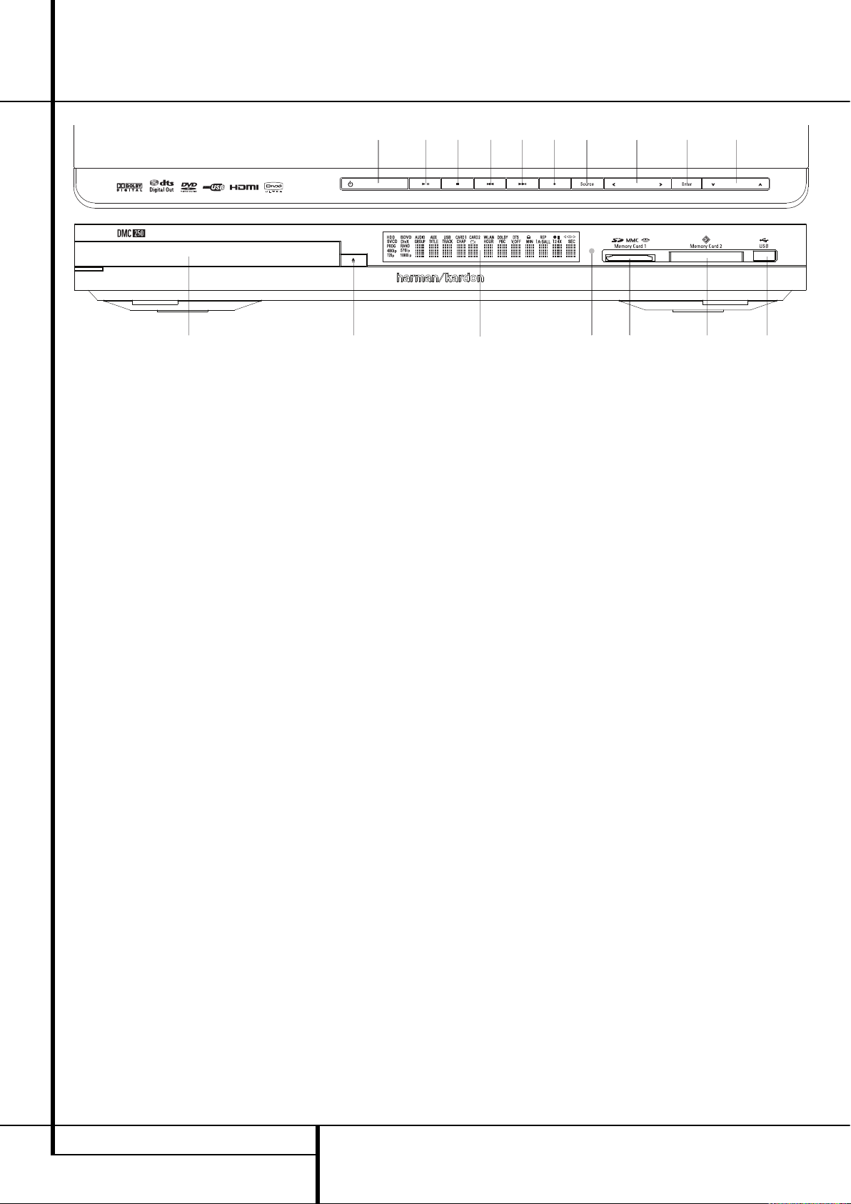
8 FRONT PANEL CONTROLS
Main Information Display: This display
delivers messages and status indications to help
you operate the DMC 250 player.
1
Power On/Off (Standby): Press the button
once to turn the DMC 250 player on, press it
again to put the unit in the Standby mode.
2
Open/Close: Press this button to open or
close the Disc Tray.
3
Disc Drawer.
4
Play/Pause: Press to initiate playback or to
resume playback after Pause has been pressed.
Press this button to momentarily pause playback. To resume playback, press the button
again. If a DVD is playing, action will freeze and
a still picture will be displayed when the button
is pressed.
5
Stop: Press this button once to place the
disc in the Resume mode, which means that
playback will stop, but as long as the tray is not
opened or the disc changed, DVD playback will
continue from the same point on the disc when
the Play Button is pressed again. Resume will
also work if the unit was turned off. To stop a
disc and have play start from the beginning,
press the button twice.
6
Skip/Search (Previous): Press this button
to move backward through the music tracks on
a CD disc or the chapters on a DVD disc. Keep
the button pressed to search backwards at one
of the available speeds.
7
Skip/Search (Next): Press to move forward
through the music tracks on a CD or the
chapters on a DVD disc. Keep the button pressed
to search forwards at one of the available
speeds.
8
Record: When an audio CD is loaded, or the
Analog Audio Inputs are selected as the source,
press this button to view the Record tab of the
on-screen menu. Pressing this button does not
begin the recording.
NOTE: It is not possible to record from one of
the memory cards or the USB device to any
other media or to the USB device. It is also not
possible to transfer image or video files.
However, an audio signal is always available at
the Analog Audio Outputs. You may make analog recordings from any source by connecting an
analog audio recorder to the rear-panel Analog
Audio Outputs.
9
Source Selector: Press this button to view
the current media source selection. If a media
source is available, that is, if media is currently
installed, the source icon will appear at normal
brightness. If no media is installed in a particular
source, e.g. if a card slot is empty, its icon will be
dimmed and you will not be able to select it. You
may always select the Disc Player or the
Auxiliary Analog Audio Inputs, even when no
media is present. Use the
M/N
Buttons to scroll
through the available sources, and press the
Enter Button to select and switch to the highlighted source.
NOTE: It is not possible to select a new source
while the current source is playing or even while
it is paused. Press the Stop Button before selecting a new source.
ABM
/N/K/LNavigation and Enter
Buttons: Use these buttons to navigate the on-
screen menus, and press the Enter Button to
select an item.
The
M/N
Buttons may be used to switch
between the track or file list on the left side of
the screen and the settings on the right side.
Press and hold a Navigation Button to scroll at a
faster rate.
When a folder is highlighted, press the Enter
Button to expand it.
Highlight the “Up” line and press the Enter
Button to close a folder and view the contents
of the next higher level of the disc, card or
device.
When a file or track is highlighted, press the
Enter Button to begin playback.
C
Card Slot 1: Insert an SD, MMC or Memory
Stick memory card into this slot by gently
pushing it all the way in until it clicks. The slot
also accommodates miniSD, microSD and
Memory Stick Duo cards when used with the
appropriate adapter, available in most
electronics and computer stores. Remove a card
from this slot by gently pushing it in until it
unlatches, then pulling it all the way out of the
slot.
D
Card Slot 2: Insert a Compact Flash I
memory card into this slot by gently pushing it
all the way in until it is firmly seated in the slot.
Remove it by pulling it all the way out of the
slot.
E
USB Port: Insert a USB client device’s
connector into this port, being careful to
correctly align the device’s plastic tongue with
the gap. Do not connect a computer to this port.
F
Remote IR Sensor.
Main Information Display
1
Power On/Off (Standby)
2
Open/Close
3
Disc Drawer
4
Play/Pause
5
Stop
6
Skip/Search (Previous)
7
Skip/Search (Next)
8
Record
9
Source Selector
A
Navigation Buttons
B
Enter
C
Card Slot 1
D
Card Slot 2
E
USB Port
F
Remote IR Sensor
1
3
876549ABA
2 EDCF
Front Panel Controls
harman/kardon
DMC250/230 Service Manual
Page 4 of 110
Page 5
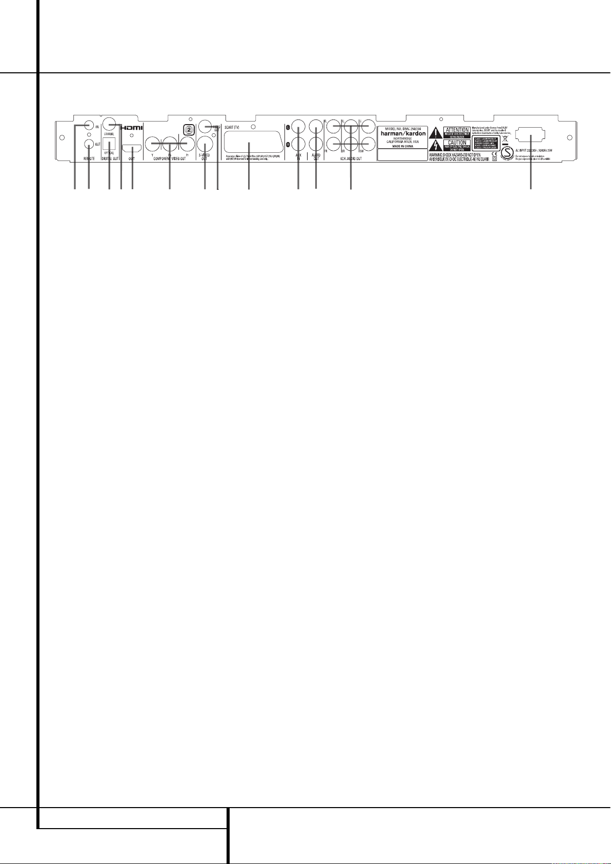
12 REAR PANEL CONNECTIONS
Rear Panel Connections
6
0
Optical Digital Output
1
Coaxial Digital Output
2
AC Power Cord
3
Composite Video Output
4
S-Video Output
5
Component Video Outputs
6
Scart TV Output
7
Remote Control Output
8
Remote Control Input
9
Analog Audio Output
A
HDMI Output
B
6-Channel Audio Outputs
C
Analog Audio Input
0
Optical Digital Output: Connect this jack
to the optical digital input of an A/V receiver or
surround processor for Dolby Digital, DTS or
PCM audio playback.
1
Coaxial Digital Output: Connect this jack
to the coaxial digital input of an A/V receiver or
surround processor for Dolby Digital, DTS or
PCM audio playback.
NOTE: The coaxial digital output should only be
connected to a digital input. Even though it is
the same RCA-type connector as standard
analog audio connections, DO NOT connect it to
a conventional analog input jack.
Connect either the Optical Digital Audio
Output
0
or the Coaxial Digital Audio
Output
1
to a corresponding digital audio
input on your receiver or processor, but not both.
2
AC Power Cord: Connect this plug to an
AC outlet. If the outlet is controlled by a switch,
make certain that it is in the ON position.
3
Composite Video Output: Connect this
jack to the video input on a television or video
projector, or to a video input on an A/V receiver
or processor if you are using that type of device
for video input switching.
4
S-Video Output: Connect this jack to the
S-Video input on a television or video projector,
or to an S-Video input on an A/V receiver or
processor if you are using that type of device for
S-Video input switching.
5
Component Video Outputs: These outputs carry the component video signals for
connection to display monitors with component
video inputs. For standard analog TV's or
projectors with inputs marked Y/Pr/Pb or
Y/Cr/Cb, connect these outputs to the corresponding inputs. If you have a high-definition television or projector that is compatible with high
scan rate progressive video, connect these jacks
to the “HD Component” inputs. Note that if you
are using a progressive scan display device, then
”Progressive” must be selected in the Video
Set-up Menu in order to take advantage of the
progressive scan circuitry. See page 22 for more
information on progressive scan video.
IMPORTANT: These jacks should NOT be
connected to standard composite video inputs.
6
SCART OUT (TV): If your TV has a SCART
socket, you can connect a SCART cable to your
TV and to your DMC 250 Player for improved
video quality. The SCART cable carries both
audio and video. You can select Composite Video
or RGB video for that SCART connector’s video
output signal.
7
Remote Control Output: Connect this
jack to the infrared (IR) input jack of another
compatible Harman Kardon remote controlled
product to have the built-in Remote Sensor on
the DMC 250 provide IR signals to other compatible products.
8
Remote Control Input: Connect the
output of a remote infrared sensor, or the
remote control output of another compatible
Harman Kardon product, to this jack. This will
enable the remote control to operate even when
the front panel Remote Sensor on the
DMC 250 is blocked. This jack may also be used
with compatible IR remote control-based
automation systems.
9
Analog Audio Output: Connect these
jacks to an audio input on an A/V receiver or
surround processor for analog audio playback.
A
HDMI Output: If you have an HDMI-compatible receiver or video display device, connect
this output to an HDMI input on the receiver or
video display for the highest-quality uncompressed digital audio and video available. Even if
your receiver is not capable of processing audio
in the HDMI format, you may still experience the
superb reproduction of HDMI video.
If your video display has a DVI input, you may
use an optional HDMI-to-DVI cable or adapter
for the connection to the display. In all cases, the
video display must be HDCP-compliant in order
to use the HDMI output. For best results, we do
not recommend HDMI connections in excess of
ten feet.
The following audio formats may be output via
the HDMI connection:
Audio CD – 2-Channel PCM or 5.1-channel DTS
DVD-Audio – 2-Channel or 5.1-channel PCM
DVD-Video – Up to 5.1-channel Dolby Digital or
DTS
Note: To hear the high-resolution surround
sound recorded on DVD-Audio discs, you need
to connect the 6-Channel Audio Outputs
B
to the corresponding input jacks on your receiver
or processor. These formats are not output digitally.
B
6-Channel Audio Outputs: Connect these
outputs to the matching 6-channel analog audio
inputs on your receiver or surround sound
processor. This connection is required to listen to
the multichannel tracks on DVD-Audio discs. If
the disc also contains a linear PCM, Dolby
Digital or DTS track, you may listen to it using
the HDMI
A
, Optical 0or Coaxial Dgital
Audio Output
1
or the Analog Audio
Outputs
9
.
Note: You’ll find more details about all
Audio/Video connections under Setup and
Connections on the following pages.
C
Analog Audio Inputs: Connect these jacks
to an audio output on a source player like a tape
deck or record player for analog audio recording.
harman/kardon
DMC250/230 Service Manual
Page 5 of 110
0
8
7
1
A
5
4
3
9C
B
2
Page 6
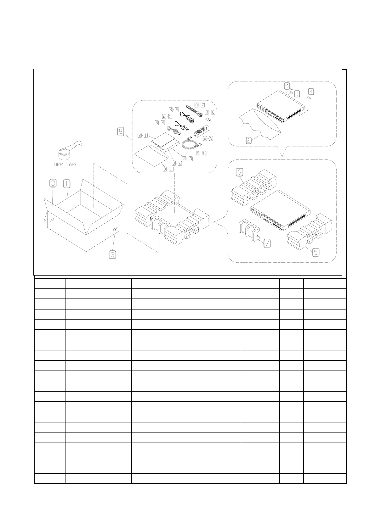
4. PACKING VIEW
harman/kardon
DMC250/230 Service Manual
Page 6 of 110
4.2 DMC250/230
Ref. No. Part No. Part Name Remarks Q'ty
1 CPG1A826Y BOX , OUT CARTON 1
2 CPB1A180Z BAG, POLY(SET) 1
3 CQB1A551Z LABEL, BAR CODE 3
4 CQB1A857Z LABEL, DTS 1
5 CPS1A759 PAD, SNOW-R 1
6 CPS1A758 PAD, SNOW-L 1
7 CPS1A765 PAD, CENTER 1
8 CQXDMC250/230 INSTRUCTION MANUAL ASS'Y 1
8-1 CQX1A1258Z MANUAL , INSTRUCTION 1
8-2 HQE1A273Z HARMAN IMAGE BROCHURES 1
8-3 CJS0I006Z CABLE, S-VHS(1.5M) 1
8-4 CJS9D002Z CORD , JACK(MONO) 1200MM 1
8-5 CJS4S004Z CORD , PIN(3P,W/R/Y) 1
8-6 CJA2B020Z CORD , POWER 1
8-7 CABR6P BATTERY (SIZE 'AA') 2
8-8 CARTDMC250 REMOCON ASS'Y 1
8-9 CJS8T001Z CABLE, HDMI(2M) 1
8-10 CPB1061W BAG, POLY(MANUAL) 1
9 CQB1A741Z LABEL, ORIGIN 1
NEW
Page 7
harman/kardon
DMC250/230 Service Manual
Page 7 of 110
Page 8

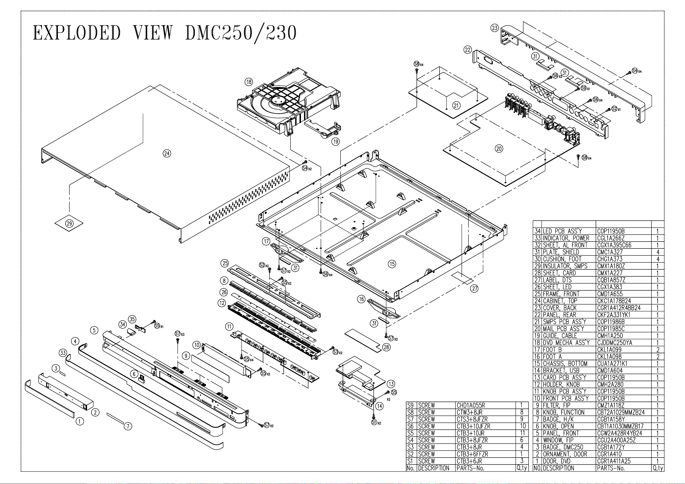
DMC 250/230 ELECTRICAL PARTS LIST
harman/kardon
DMC250/230 Service Manual
Page 8 of 110
Ref# Component Description Value
CHE154 CLAMPER , ARM
CPG1A826Y BOX , OUT CARTON DMC250/230
CPS1A758 PAD , SNOW(L)
CPS1A759 PAD , SNOW(R)
CPS1A765 PAD , CENTER DMC250
CQB1A549Y LABEL , ATTENTION DVD48
CQB1A551Z LABEL , BAR CODE
CQB1A622 LABEL , SERIAL NO
CQB1A741Z ORIGIN LABEL
CQB1A744Z LABEL, DIVX
CQB1A876Z LABEL , COUNTRY DVD29/230
CQXDMC250/230 INSTRUCTION MANUAL ASS'Y
CARTDMC250 REMOCON ASS'Y
CJA2B020Z CORD , POWER
CJS0I006Z CABLE, S-VHS(1.5M) Y, C
CJS4S004Z CORD , PIN(3P,W/R/Y)
CJS8T001Z CABLE, HDMI(2M) CBADV-005-2
CJS9D002Z CORD , JACK(MONO) 1200MM
CQX1A1258Z MANUAL , INSTRUCTION DMC250/230
CGR1A411ZA DVD DOOR ASS'Y(DMC250) DMC250
CGR1A410 ORNAMENT , DOOR
CGR1A411A25 DOOR , DVD
CGR1A412R4B24 COVER , BACK DMC250
CGWDMC250/230 FRONT PANEL ASS'Y
CBT2A1029ZA FUNCTION KNOB ASS'Y
CBT2A1029MMZB24 KNOB , FUNCTION DMC250
CGX1A383Z SHEET , LED
CMH2A280 HOLDER , KNOB
CGB1A158Y BADGE , FRONT HARMAN/KARDON
CGB1A172Y BADGE , DMC250
CGL1A266Y INDICATOR , POWER DVD29
CGW2A428YA DMC250/230 FRONT PANEL ASS'Y
CBT1A1030MMZB17 KNOB , OPEN
CGU1A400A25Z WINDOW , FIP
CGW2A428R4YB24 PANEL , FRONT DMC250/230
CGX1A385 COVER , SHEET DMC250
CGX1A395C66 SHEET , AL FRONT DMC250
CHG1A305 CUSHION , SUPPORT
CMC1A341 PLATE , EARTH DMC250
CMD1A604 BRACKET , USB
CMD1A655 FRAME , FRONT
CMD1A682 BRACKET , HOLDER
CMX1A227 SHEET , CARD DMC250
CMZ1A118Z FILTER , FIP
COP11950B FRONT/CARD PCB ASS'Y DMC250
CIP11950B FRONT/CARD AUTO PCB ASS'Y DMC250
CIP11950BSMD FRONT/CARD SMD PCB ASS'Y DMC250
CIP11950BBSMD FRONT/CARD BOTTOM SMD PCB ASS'Y DMC250
C202 CCUS1H104KC CAP , CHIP 0.1UF 50V K
C203 CCUS1H104KC CAP , CHIP 0.1UF 50V K
C214 CCUS1H104KC CAP , CHIP 0.1UF 50V K
C217 CCUS1H102KC CAP , CHIP 1000PF 50V K
C333 CCUS1H220JA CAP , CHIP 22PF 50V J
C334 CCUS1H220JA CAP , CHIP 22PF 50V J
C335 CCUS1H220JA CAP , CHIP 22PF 50V J
C336 CCUS1H220JA CAP , CHIP 22PF 50V J
C337 CCUS1H220JA CAP , CHIP 22PF 50V J
C904 CCUS1H104KC CAP , CHIP 0.1UF 50V K
R203 CRJ10DJ681T RES , CHIP 1608 SIZE
R204 CRJ10DJ103T RES , CHIP 1608 SIZE
R205 CRJ10DJ331T RES , CHIP
R227 CRJ10DJ333T RES , CHIP 1608 SIZE
R228 CRJ10DJ100T RES , CHIP 1608 SIZE
R229 CRJ10DJ103T RES , CHIP 1608 SIZE
R905 CRJ104DJ301T RES , ARRAY 300R (1608*4)
R906 CRJ104DJ301T RES , ARRAY 300R (1608*4)
R907 CRJ104DJ301T RES , ARRAY 300R (1608*4)
R909 CRJ104DJ301T RES , ARRAY 300R (1608*4)
R910 CRJ104DJ301T RES , ARRAY 300R (1608*4)
Page 9

R911 CRJ104DJ301T RES , ARRAY 300R (1608*4)
harman/kardon
DMC250/230 Service Manual
Page 9 of 110
R912 CRJ104DJ301T RES , ARRAY 300R (1608*4)
R913 CRJ104DJ301T RES , ARRAY 300R (1608*4)
R914 CRJ104DJ301T RES , ARRAY 300R (1608*4)
R921 CRJ10DJ103T RES , CHIP 1608 SIZE
R923 CRJ10DJ103T RES , CHIP 1608 SIZE
R924 CRJ10DJ301T RES , CHIP 1608
R927 CRJ10DJ301T RES , CHIP 1608
R930 CRJ10DJ301T RES , CHIP 1608
R931 CRJ10DJ301T RES , CHIP 1608
CIP11950BTSMD FRONT/CARD TOP SMD PCB ASS'Y DMC250
CUP11950Z PCB , FRONT/CRAD DMC250 330X170(FR-4/2 LAYER)
CN27 CJP50GA205ZM WAFER , MOLEX 51374 50PIN, 0.5mm STRAIGHT MOLEX 51374 50PIN, 0.5MM
C201 CCUS1H104KC CAP , CHIP 0.1UF 50V K
C216 CCUS1H104KC CAP , CHIP 0.1UF 50V K
C331 CCUS1H221JA CAP , CHIP 220PF 50V J
C332 CCUS1H221JA CAP , CHIP 220PF 50V J
C902 CCUS1H680JA CAP , CHIP 68PF 50V J
C903 CCUS1H680JA CAP , CHIP 68PF 50V J
C909 CCUS1H104KC CAP , CHIP 0.1UF 50V K
C910 CCUS1H104KC CAP , CHIP 0.1UF 50V K
C911 CCUS1H104KC CAP , CHIP 0.1UF 50V K
C912 CCUS1H104KC CAP , CHIP 0.1UF 50V K
C914 CCUS1H104KC CAP , CHIP 0.1UF 50V K
C915 CCUS1H104KC CAP , CHIP 0.1UF 50V K
C918 CCUS1H104KC CAP , CHIP 0.1UF 50V K
C919 CCUS1H104KC CAP , CHIP 0.1UF 50V K
C922 CCUS1H104KC CAP , CHIP 0.1UF 50V K
C923 CCUS1H104KC CAP , CHIP 0.1UF 50V K
C924 CCUS1H104KC CAP , CHIP 0.1UF 50V K
D301 HVDRLS4148SR DIODE, SWITCHING, SMD TYPE RLS4148 TE-11
FB91 HLZ9R001Z FB, 2012(0805)600E, 1.5A,POWER 600E, 1.5A
FB93 HLZ9R001Z FB, 2012(0805)600E, 1.5A,POWER 600E, 1.5A
IC91 HVITC4053BF IC , 2CH. MULTI/DEMULTIPLXER TC4053BF (TAPE)
IC92 HVITC4053BF IC , 2CH. MULTI/DEMULTIPLXER TC4053BF (TAPE)
IC93 CVIKIA1117S33 I.C , REGULATOR(SOT-223) KIA1117S/F33, SOT-223
IC94 CVIRT9702APB IC , CURRENT LIMITER
JK16 CJJ9Y001Z JACK , CF CARD SOCKET RJ-006TC
JK17 CJJ9Y002Z JACK , CARD SOCKET(4 IN 1)
Q201 HVTKRA107ST T.R , CHIP KRA107S
R201 CRJ10DJ152T RES , CHIP 1608 SIZE
R202 CRJ10DJ222T RES , CHIP 1608 SIZE
R206 CRJ10DJ122T RES , CHIP 1608 SIZE
R207 CRJ10DJ821T RES , CHIP 1608 SIZE
R208 CRJ10DJ681T RES , CHIP 1608 SIZE
R209 CRJ10DJ122T RES , CHIP 1608 SIZE
R210 CRJ10DJ821T RES , CHIP 1608 SIZE
R211 CRJ10DJ332T RES , CHIP 1608 SIZE
R212 CRJ10DJ331T RES , CHIP
R213 CRJ10DJ222T RES , CHIP 1608 SIZE
R214 CRJ10DJ152T RES , CHIP 1608 SIZE
R215 CRJ10DJ331T RES , CHIP
R216 CRJ10DJ331T RES , CHIP
R217 CRJ10DJ331T RES , CHIP
R218 CRJ10DJ331T RES , CHIP
R219 CRJ10DJ331T RES , CHIP
R220 CRJ10DJ331T RES , CHIP
R221 CRJ10DJ331T RES , CHIP
R222 CRJ10DJ331T RES , CHIP
R223 CRJ10DJ331T RES , CHIP
R224 CRJ10DJ331T RES , CHIP
R225 CRJ10DJ331T RES , CHIP
R226 CRJ10DJ331T RES , CHIP
R901 CRJ10DJ104T RES , CHIP 1608 SIZE
R902 CRJ10DJ0R0T RES , CHIP 1608 SIZE
R903 CRJ10DJ270T RES , CHIP
R904 CRJ10DJ270T RES , CHIP
R908 CRJ10DJ0R0T RES , CHIP 1608 SIZE
R915 CRJ10DJ103T RES , CHIP 1608 SIZE
R916 CRJ10DJ103T RES , CHIP 1608 SIZE
R917 CRJ10DJ103T RES , CHIP 1608 SIZE
Page 10

R918 CRJ10DJ104T RES , CHIP 1608 SIZE
harman/kardon
DMC250/230 Service Manual
Page 10 of 110
R919 CRJ10DJ0R0T RES , CHIP 1608 SIZE
R920 CRJ104DJ301T RES , ARRAY 300R (1608*4)
R922 CRJ104DJ301T RES , ARRAY 300R (1608*4)
R925 CRJ10DJ103T RES , CHIP 1608 SIZE
R926 CRJ10DJ750T RES , CHIP 1608 SIZE
R928 CRJ104DJ301T RES , ARRAY 300R (1608*4)
R929 CRJ104DJ750T RES , ARRAY 75R (1608*4)
R932 CRJ104DJ103T RES, ARRAY, 10K (1608) 10K(1608)
R933 CRJ104DJ750T RES , ARRAY 75R (1608*4)
R934 CRJ104DJ103T RES, ARRAY, 10K (1608) 10K(1608)
R935 CRJ10DJ750T RES , CHIP 1608 SIZE
R936 CRJ10DJ103T RES , CHIP 1608 SIZE
R937 CRJ10DJ0R0T RES , CHIP 1608 SIZE
R938 CRJ104DJ103T RES, ARRAY, 10K (1608) 10K(1608)
R939 CRJ104DJ103T RES, ARRAY, 10K (1608) 10K(1608)
R940 CRJ10DJ0R0T RES , CHIP 1608 SIZE
R941 CRJ10DJ0R0T RES , CHIP 1608 SIZE
R942 CRJ10DJ0R0T RES , CHIP 1608 SIZE
R943 CRJ10DJ202T RES , CHIP
R944 CRJ10DJ202T RES , CHIP
R945 CRJ10DJ202T RES , CHIP
R946 CRJ10DJ202T RES , CHIP
R947 CRJ10DJ103T RES , CHIP 1608 SIZE
R951 CRJ10DJ273T RES , CHIP
R952 CRJ10DJ273T RES , CHIP
R998 CRJ10DJ220T RES , CHIP 1608 SIZE
R999 CRJ10DJ222T RES , CHIP 1608 SIZE
C213 CCEA1CKS220T CAP , ELECT 22UF 16V SMALL SIZE
C901 CCEA1HKS100T CAP , ELECT 10UF 50V SMALL SIZE
C906 CCEA1HKS100T CAP , ELECT 10UF 50V SMALL SIZE
C907 CCEA1AKS221T CAP , ELECT 220UF 10V
C908 CCEA1EKS470T CAP , ELECT 47UF 25V
C913 CCEA1EKS470T CAP , ELECT 47UF 25V
C916 CCEA1EKS470T CAP , ELECT 47UF 25V
C917 CCEA1EKS470T CAP , ELECT 47UF 25V
C920 CCEA1CKS101T CAP , ELECT 100UF 16V
C921 CCEA1CKS101T CAP , ELECT 100UF 16V
D901 CVD1N4003SRT DIODE , RECT 1N4003
SW11 CST1A012ZT SW , TACT SKHV10910G
SW12 CST1A012ZT SW , TACT SKHV10910G
SW13 CST1A012ZT SW , TACT SKHV10910G
SW14 CST1A012ZT SW , TACT SKHV10910G
SW15 CST1A012ZT SW , TACT SKHV10910G
SW16 CST1A012ZT SW , TACT SKHV10910G
SW17 CST1A012ZT SW , TACT SKHV10910G
SW18 CST1A012ZT SW , TACT SKHV10910G
SW19 CST1A012ZT SW , TACT SKHV10910G
SW20 CST1A012ZT SW , TACT SKHV10910G
SW21 CST1A012ZT SW , TACT SKHV10910G
SW22 CST1A012ZT SW , TACT SKHV10910G
SW23 CST1A012ZT SW , TACT SKHV10910G
CMD2A602 BRACKET , FL
BN31 CWZDMC250BN31 SHIEL WIRE ASS'Y(4P, 200mm)
BN99 CWB1C903180EN WIRE ASS'Y (3P, 180mm)
CN18 CJP17GB113ZY WAFER
CN33 CJP09GB113ZY WAFER , 9PIN ANGLE CARD CABLE 1MM
CN34 CJP09GB113ZY WAFER , 9PIN ANGLE CARD CABLE 1MM
CN99 CJP03GB46ZY WAFER , ANGLE(3PIN)
D201 CVD1L0345W31BOCT20 L.E.D , WHITE 1L0345W31BOCT201
D202 CVD1L0345W31BOCT20 L.E.D , WHITE 1L0345W31BOCT201
D203 CVD1L0345W31BOCT20 L.E.D , WHITE 1L0345W31BOCT201
D204 CVD1L0345W31BOCT20 L.E.D , WHITE 1L0345W31BOCT201
D205 CVD1L0345W31BOCT20 L.E.D , WHITE 1L0345W31BOCT201
D206 CVD1L034FA22M0MA L.E.D , AMBER DIFFUSED 1L034FA22M0MA001
D207 CVD1L0345W31BOCT20 L.E.D , WHITE 1L0345W31BOCT201
D208 CVD1L0345W31BOCT20 L.E.D , WHITE 1L0345W31BOCT201
D209 CVD30BSOKTAAU4 L.E.D , SUPER ORANGE(3PAI, 2.5mm/BULK) TOL-30BSOKTAA-U4
D210 CVD1L0345W31BOCT20 L.E.D , WHITE 1L0345W31BOCT201
D211 CVD1L0345W31BOCT20 L.E.D , WHITE 1L0345W31BOCT201
D212 CVD1L0345W31BOCT20 L.E.D , WHITE 1L0345W31BOCT201
Page 11

D213 CVD1L0345W31BOCT20 L.E.D , WHITE 1L0345W31BOCT201
harman/kardon
DMC250/230 Service Manual
Page 11 of 110
D214 CVD1L0345W31BOCT20 L.E.D , WHITE 1L0345W31BOCT201
D998 CVD1L0345W31BOCT20 L.E.D , WHITE 1L0345W31BOCT201
D999 CVD1L034FA22M0MA L.E.D , AMBER DIFFUSED 1L034FA22M0MA001
FIP1 CFL13BT231GINK F.I.P , FUTABA
IC21 HRVKSM603TH2 SENSOR , REMOCON KSM-603TH2
JK13 HJJ9X001Z JACK, USB
JW14 CWE8202080RV WIRE ASS'Y(1P)
JW21 CWE7202100AR WIRE ASS'Y
JW22 CWE8202080RV WIRE ASS'Y(1P)
JW23 CWE8202080RV WIRE ASS'Y(1P)
CTB3+10JR SCREW
CTB3+6JR SCREW
CTB3+8JR SCREW
CTS3+8JFZR SCREW
CWE7202050RR WIRE ASS'Y
CWE8102050RR RING WIRE ASS'Y
C4FA031 TAPE , BOTH SIDE NITTO #500
KMC1A267 TAPE , EMI GASKET
CKC1A178S60 CABINET, TOP DMC250
CMC1A327 PLATE , SHIELD
CMX1A180Z INSULATOR
CTB3+6JR SCREW
CTB3+8JFZR SCREW
CTS3+8JFZR SCREW
CUADMC250/230 BOTTOM CHASSIS ASS'Y
CHD1A055R SCREW , SPECIAL
CHG1A373 CUSHION , FOOT AVR350
CJDDMC250YA DVD MECHANISM ASS'Y
CADSDL003WA DVD LOADER ASS'Y
CADSDL003Z LOADER
CJDDV348HG TRAVERSE PICKUP ASS'Y SF-HD850HG
CMH1A250 GUIDE, CABLE
CWB1B905150EE WIRE ASS'Y
CWB5A906150SE WIRE ASS'Y
CWC4G2A24G300B CABLE , CARD DVD(0.5mm PITCH, A-B) DMC250
CKF2A331YK1 PANEL , REAR DMC250/230
CKL1A098 FOOT , L
CKL1A099 FOOT , R
COP11985C DMC250/230 MAIN PCB ASS'Y
C101 CCUS1H104KC CAP , CHIP 0.1UF 50V K
C102 CCUS1H104KC CAP , CHIP 0.1UF 50V K
C103 CCUS1H104KC CAP , CHIP 0.1UF 50V K
C104 CCUS1H104KC CAP , CHIP 0.1UF 50V K
C108 CCUS1H104KC CAP , CHIP 0.1UF 50V K
C110 CCUS1H104KC CAP , CHIP 0.1UF 50V K
C111 CCUS1H104KC CAP , CHIP 0.1UF 50V K
C112 CCUS1H104KC CAP , CHIP 0.1UF 50V K
C113 CCUS1H104KC CAP , CHIP 0.1UF 50V K
C116 CCUS1H103KC CAP , CHIP 0.01UF 50V K
C117 CCUS1H103KC CAP , CHIP 0.01UF 50V K
C118 CCUS1H103KC CAP , CHIP 0.01UF 50V K
C119 CCUS1H103KC CAP , CHIP 0.01UF 50V K
C120 CCUS1H103KC CAP , CHIP 0.01UF 50V K
C122 CCUS1H103KC CAP , CHIP 0.01UF 50V K
C123 CCUS1H103KC CAP , CHIP 0.01UF 50V K
C124 CCUS1H101JA CAP , CHIP 100PF 50V J
C130 CCUS1H103KC CAP , CHIP 0.01UF 50V K
C131 CCUS1H103KC CAP , CHIP 0.01UF 50V K
C132 CCUS1H103KC CAP , CHIP 0.01UF 50V K
C133 CCUS1H103KC CAP , CHIP 0.01UF 50V K
C134 CCUS1H103KC CAP , CHIP 0.01UF 50V K
C135 CCUS1H103KC CAP , CHIP 0.01UF 50V K
C136 CCUS1H103KC CAP , CHIP 0.01UF 50V K
C137 CCUS1H103KC CAP , CHIP 0.01UF 50V K
C138 CCUS1H103KC CAP , CHIP 0.01UF 50V K
C139 CCUS1H103KC CAP , CHIP 0.01UF 50V K
C140 CCUS1H103KC CAP , CHIP 0.01UF 50V K
C141 CCUS1H103KC CAP , CHIP 0.01UF 50V K
C142 CCUS1H103KC CAP , CHIP 0.01UF 50V K
C143 CCUS1H103KC CAP , CHIP 0.01UF 50V K
Page 12

C144 CCUS1H103KC CAP , CHIP 0.01UF 50V K
harman/kardon
DMC250/230 Service Manual
Page 12 of 110
C145 CCUS1H103KC CAP , CHIP 0.01UF 50V K
C146 CCUS1H103KC CAP , CHIP 0.01UF 50V K
C147 CCUS1H103KC CAP , CHIP 0.01UF 50V K
C148 CCUS1H101JA CAP , CHIP 100PF 50V J
C155 CCUS1H102KC CAP , CHIP 1000PF 50V K
C156 CCUS1H102KC CAP , CHIP 1000PF 50V K
C157 CCUS1H273KC CAP , CHIP 0.027UF 50V K
C158 CCUS1H273KC CAP , CHIP 0.027UF 50V K
C166 CCUS1H104KC CAP , CHIP 0.1UF 50V K
C180 CCUS1H102KC CAP , CHIP 1000PF 50V K
C185 CCUS1H104KC CAP , CHIP 0.1UF 50V K
C186 CCUS1H104KC CAP , CHIP 0.1UF 50V K
C195 CCUS1H050CA CAP , CHIP 5PF 50V C
C281 CCUS1H030CA CAP , CHIP(50V/3PF)
C282 CCUS1H030CA CAP , CHIP(50V/3PF)
C283 CCUS1H030CA CAP , CHIP(50V/3PF)
C284 CCUS1H030CA CAP , CHIP(50V/3PF)
C285 CCUS1H030CA CAP , CHIP(50V/3PF)
C286 CCUS1H030CA CAP , CHIP(50V/3PF)
C287 CCUS1H030CA CAP , CHIP(50V/3PF)
C288 CCUS1H030CA CAP , CHIP(50V/3PF)
C311 CCUS1H104KC CAP , CHIP 0.1UF 50V K
C312 CCUS1H104KC CAP , CHIP 0.1UF 50V K
C313 CCUS1H104KC CAP , CHIP 0.1UF 50V K
C314 CCUS1H104KC CAP , CHIP 0.1UF 50V K
C315 CCUS1H104KC CAP , CHIP 0.1UF 50V K
C316 CCUS1H104KC CAP , CHIP 0.1UF 50V K
C317 CCUS1H104KC CAP , CHIP 0.1UF 50V K
C318 CCUS1H104KC CAP , CHIP 0.1UF 50V K
C319 CCUS1H104KC CAP , CHIP 0.1UF 50V K
C320 CCUS1H104KC CAP , CHIP 0.1UF 50V K
C321 CCUS1H104KC CAP , CHIP 0.1UF 50V K
C322 CCUS1H104KC CAP , CHIP 0.1UF 50V K
C323 CCUS1H104KC CAP , CHIP 0.1UF 50V K
C325 CCUS1H104KC CAP , CHIP 0.1UF 50V K
C326 CCUS1H104KC CAP , CHIP 0.1UF 50V K
C327 CCUS1H104KC CAP , CHIP 0.1UF 50V K
C328 CCUS1H104KC CAP , CHIP 0.1UF 50V K
C329 CCUS1H104KC CAP , CHIP 0.1UF 50V K
C330 CCUS1H104KC CAP , CHIP 0.1UF 50V K
C331 CCUS1H104KC CAP , CHIP 0.1UF 50V K
C332 CCUS1H104KC CAP , CHIP 0.1UF 50V K
C333 CCUS1H104KC CAP , CHIP 0.1UF 50V K
C334 CCUS1H104KC CAP , CHIP 0.1UF 50V K
C335 CCUS1H104KC CAP , CHIP 0.1UF 50V K
C336 CCUS1H104KC CAP , CHIP 0.1UF 50V K
C337 CCUS1H104KC CAP , CHIP 0.1UF 50V K
C338 CCUS1H104KC CAP , CHIP 0.1UF 50V K
C339 CCUS1H104KC CAP , CHIP 0.1UF 50V K
C340 CCUS1H104KC CAP , CHIP 0.1UF 50V K
C341 CCUS1H104KC CAP , CHIP 0.1UF 50V K
C342 CCUS1H104KC CAP , CHIP 0.1UF 50V K
C343 CCUS1H104KC CAP , CHIP 0.1UF 50V K
C344 CCUS1H104KC CAP , CHIP 0.1UF 50V K
C345 CCUS1H104KC CAP , CHIP 0.1UF 50V K
C346 CCUS1H104KC CAP , CHIP 0.1UF 50V K
C347 CCUS1H104KC CAP , CHIP 0.1UF 50V K
C348 CCUS1H104KC CAP , CHIP 0.1UF 50V K
C354 CCUS1H104KC CAP , CHIP 0.1UF 50V K
C361 CCUS1H104KC CAP , CHIP 0.1UF 50V K
C362 CCUS1H104KC CAP , CHIP 0.1UF 50V K
C363 CCUS1H104KC CAP , CHIP 0.1UF 50V K
C369 CCUS1H104KC CAP , CHIP 0.1UF 50V K
C370 CCUS1H104KC CAP , CHIP 0.1UF 50V K
C371 CCUS1H104KC CAP , CHIP 0.1UF 50V K
C372 CCUS1H104KC CAP , CHIP 0.1UF 50V K
C373 CCUS1H104KC CAP , CHIP 0.1UF 50V K
C374 CCUS1H104KC CAP , CHIP 0.1UF 50V K
C404 CCUS1H104KC CAP , CHIP 0.1UF 50V K
C406 CCUS1H104KC CAP , CHIP 0.1UF 50V K
Page 13

C408 CCUS1H104KC CAP , CHIP 0.1UF 50V K
harman/kardon
DMC250/230 Service Manual
Page 13 of 110
C409 CCUS1H104KC CAP , CHIP 0.1UF 50V K
C426 CCUS1H104KC CAP , CHIP 0.1UF 50V K
C604 CCUS1H104KC CAP , CHIP 0.1UF 50V K
C606 CCUS1H104KC CAP , CHIP 0.1UF 50V K
C612 CCUS1H104KC CAP , CHIP 0.1UF 50V K
C618 CCUS1H104KC CAP , CHIP 0.1UF 50V K
C663 CCUS1H104KC CAP , CHIP 0.1UF 50V K
C664 CCUS1H104KC CAP , CHIP 0.1UF 50V K
C756 CCUS1H104KC CAP , CHIP 0.1UF 50V K
C758 CCUS1H221JA CAP , CHIP 220PF 50V J
C759 CCUS1H221JA CAP , CHIP 220PF 50V J
C760 CCUS1H221JA CAP , CHIP 220PF 50V J
C803 CCUS1H104KC CAP , CHIP 0.1UF 50V K
C804 CCUS1H103KC CAP , CHIP 0.01UF 50V K
C807 CCUS1H104KC CAP , CHIP 0.1UF 50V K
C808 CCUS1H103KC CAP , CHIP 0.01UF 50V K
C811 CCUS1H104KC CAP , CHIP 0.1UF 50V K
C812 CCUS1H104KC CAP , CHIP 0.1UF 50V K
C813 CCUS1H104KC CAP , CHIP 0.1UF 50V K
C814 CCUS1H103KC CAP , CHIP 0.01UF 50V K
C816 CCUS1H104KC CAP , CHIP 0.1UF 50V K
C817 CCUS1H104KC CAP , CHIP 0.1UF 50V K
C820 CCUS1H104KC CAP , CHIP 0.1UF 50V K
C821 CCUS1H104KC CAP , CHIP 0.1UF 50V K
C824 CCUS1H104KC CAP , CHIP 0.1UF 50V K
C825 CCUS1H103KC CAP , CHIP 0.01UF 50V K
C826 CCUS1H104KC CAP , CHIP 0.1UF 50V K
C827 CCUS1H104KC CAP , CHIP 0.1UF 50V K
C828 CCUS1H104KC CAP , CHIP 0.1UF 50V K
C829 CCUS1H104KC CAP , CHIP 0.1UF 50V K
C830 CCUS1H104KC CAP , CHIP 0.1UF 50V K
C831 CCUS1H104KC CAP , CHIP 0.1UF 50V K
C832 CCUS1H104KC CAP , CHIP 0.1UF 50V K
C833 CCUS1H104KC CAP , CHIP 0.1UF 50V K
C841 CCUS1H104KC CAP , CHIP 0.1UF 50V K
C842 CCUS1H104KC CAP , CHIP 0.1UF 50V K
C843 CCUS1H104KC CAP , CHIP 0.1UF 50V K
C844 CCUS1H104KC CAP , CHIP 0.1UF 50V K
C845 CCUS1H104KC CAP , CHIP 0.1UF 50V K
C846 CCUS1H104KC CAP , CHIP 0.1UF 50V K
C848 CCUS1H104KC CAP , CHIP 0.1UF 50V K
C849 CCUS1H104KC CAP , CHIP 0.1UF 50V K
C850 CCUS1H104KC CAP , CHIP 0.1UF 50V K
C851 CCUS1H104KC CAP , CHIP 0.1UF 50V K
C852 CCUS1H104KC CAP , CHIP 0.1UF 50V K
C853 CCUS1H104KC CAP , CHIP 0.1UF 50V K
C904 CCSJA0J220B CAP , CHIP TANTAL(A TYPE, 22uF/6.3V, ELNA)
C905 CCUS1H104KC CAP , CHIP 0.1UF 50V K
C906 CCUS1H102KC CAP , CHIP 1000PF 50V K
C907 CCUS1H102KC CAP , CHIP 1000PF 50V K
C911 CCSJA0J220B CAP , CHIP TANTAL(A TYPE, 22uF/6.3V, ELNA)
C912 CCUS1H104KC CAP , CHIP 0.1UF 50V K
C913 CCUS1H102KC CAP , CHIP 1000PF 50V K
C914 CCUS1H102KC CAP , CHIP 1000PF 50V K
C915 CCUS1H102KC CAP , CHIP 1000PF 50V K
C916 CCSJA0J220B CAP , CHIP TANTAL(A TYPE, 22uF/6.3V, ELNA)
C917 CCUS1H104KC CAP , CHIP 0.1UF 50V K
C918 CCUS1H102KC CAP , CHIP 1000PF 50V K
C919 CCUS1H102KC CAP , CHIP 1000PF 50V K
C920 CCUS1H102KC CAP , CHIP 1000PF 50V K
C923 CCSJA1C100B CAP , CHIP TANTAL(A TYPE, 10uF/16V, ELNA)
C924 CCUS1H104KC CAP , CHIP 0.1UF 50V K
C925 CCSJA1C100B CAP , CHIP TANTAL(A TYPE, 10uF/16V, ELNA)
C930 CCUS1H104KC CAP , CHIP 0.1UF 50V K
C931 CCUS1H104KC CAP , CHIP 0.1UF 50V K
C933 CCUS1H104KC CAP , CHIP 0.1UF 50V K
C945 CCSJA0J220B CAP , CHIP TANTAL(A TYPE, 22uF/6.3V, ELNA)
C952 CCUS1H104KC CAP , CHIP 0.1UF 50V K
C953 CCUS1H104KC CAP , CHIP 0.1UF 50V K
C956 CCUS1H221JA CAP , CHIP 220PF 50V J
Page 14

FB13 HLZ9R001Z FB, 2012(0805)600E, 1.5A,POWER 600E, 1.5A
harman/kardon
DMC250/230 Service Manual
Page 14 of 110
FB24 HLZ9R001Z FB, 2012(0805)600E, 1.5A,POWER 600E, 1.5A
FB45 HLZ9R001Z FB, 2012(0805)600E, 1.5A,POWER 600E, 1.5A
L509 HLZ9R001Z FB, 2012(0805)600E, 1.5A,POWER 600E, 1.5A
L607 HLZ9R005Z BEAD CHIP 60(1608 SIZE) HH-1M1608-600
L901 HLZ9R001Z FB, 2012(0805)600E, 1.5A,POWER 600E, 1.5A
R11 CRJ10DJ0R0T RES , CHIP 1608 SIZE
R112 CRJ10DJ103T RES , CHIP 1608 SIZE
R137 CRJ10DJ202T RES , CHIP
R138 CRJ10DJ202T RES , CHIP
R141 CRJ10DJ330T RES , CHIP 1608 SIZE
R143 CRJ10DF2002T RES , CHIP 1%
R151 CRJ10DF39R0T CHIP RES, 1% 39 Ohm
R152 CRJ10DF4300T RES
R198 CRJ10DJ0R0T RES , CHIP 1608 SIZE
R199 CRJ10DJ0R0T RES , CHIP 1608 SIZE
R215 CRJ10DJ472T RES , CHIP 1608 SIZE
R321 CRJ10DJ103T RES , CHIP 1608 SIZE
R322 CRJ10DJ103T RES , CHIP 1608 SIZE
R348 CRJ10DJ103T RES , CHIP 1608 SIZE
R350 CRJ104DJ101T RES , CHIP NETWORK(1/16W, 100ohm, 1608X4) 100R (1608)
R351 CRJ10DJ102T RES , CHIP 1608 SIZE
R352 CRJ10DJ102T RES , CHIP 1608 SIZE
R353 CRJ10DJ102T RES , CHIP 1608 SIZE
R354 CRJ10DJ102T RES , CHIP 1608 SIZE
R355 CRJ10DJ102T RES , CHIP 1608 SIZE
R356 CRJ10DJ102T RES , CHIP 1608 SIZE
R357 CRJ10DJ102T RES , CHIP 1608 SIZE
R379 CRJ10DJ103T RES , CHIP 1608 SIZE
R380 CRJ10DJ0R0T RES , CHIP 1608 SIZE
R436 CRJ10DJ103T RES , CHIP 1608 SIZE
R735 CRJ10DJ0R0T RES , CHIP 1608 SIZE
R752 CRJ10DJ103T RES , CHIP 1608 SIZE
R753 CRJ10DJ103T RES , CHIP 1608 SIZE
R761 CRJ10DJ103T RES , CHIP 1608 SIZE
R762 CRJ10DJ0R0T RES , CHIP 1608 SIZE
R763 CRJ10DJ0R0T RES , CHIP 1608 SIZE
R797 CRJ10DJ473T RES , CHIP 1608 SIZE
R798 CRJ10DJ473T RES , CHIP 1608 SIZE
R810 CRJ10DJ0R0T RES , CHIP 1608 SIZE
R811 CRJ10DJ0R0T RES , CHIP 1608 SIZE
R812 CRJ10DJ0R0T RES , CHIP 1608 SIZE
R822 CRJ10DJ0R0T RES , CHIP 1608 SIZE
R824 CRJ10DJ0R0T RES , CHIP 1608 SIZE
R835 CRJ10DJ472T RES , CHIP 1608 SIZE
R842 CRJ10DJ0R0T RES , CHIP 1608 SIZE
R844 CRJ10DJ0R0T RES , CHIP 1608 SIZE
R893 CRJ10DJ0R0T RES , CHIP 1608 SIZE
R912 CRJ10DJ472T RES , CHIP 1608 SIZE
R913 CRJ10DF4700T RES, CHIP 470 OHM/1608/1%
R919 CRJ10DJ473T RES , CHIP 1608 SIZE
CN20 CJP24GA195ZM SMT FFC/FPC WAFER(0.5MM PITCH) 52559-2472 (PB FREE)
CN26 CJP50GA205ZM WAFER , MOLEX 51374 50PIN, 0.5mm STRAIGHT MOLEX 51374 50PIN, 0.5MM
C106 CCUS1H102KC CAP , CHIP 1000PF 50V K
C109 CCUS1H104KC CAP , CHIP 0.1UF 50V K
C121 CCUS1H103KC CAP , CHIP 0.01UF 50V K
C126 CCUS1H103KC CAP , CHIP 0.01UF 50V K
C127 CCUS1H103KC CAP , CHIP 0.01UF 50V K
C151 CCUS1H330JA CAP , CHIP 33PF 50V J
C152 CCUS1H330JA CAP , CHIP 33PF 50V J
C153 CCUS1H330JA CAP , CHIP 33PF 50V J
C154 CCUS1H330JA CAP , CHIP 33PF 50V J
C162 CCUS1H330JA CAP , CHIP 33PF 50V J
C165 CCUS1H104KC CAP , CHIP 0.1UF 50V K
C167 CCUS1H102KC CAP , CHIP 1000PF 50V K
C168 CCUS1H330JA CAP , CHIP 33PF 50V J
C169 CCUS1H330JA CAP , CHIP 33PF 50V J
C170 CCUS1H330JA CAP , CHIP 33PF 50V J
C171 CCUS1H330JA CAP , CHIP 33PF 50V J
C172 CCUS1H330JA CAP , CHIP 33PF 50V J
C173 CCUS1H330JA CAP , CHIP 33PF 50V J
Page 15

C174 CCUS1H330JA CAP , CHIP 33PF 50V J
harman/kardon
DMC250/230 Service Manual
Page 15 of 110
C175 CCUS1H330JA CAP , CHIP 33PF 50V J
C176 CCUS1H330JA CAP , CHIP 33PF 50V J
C177 CCUS1H330JA CAP , CHIP 33PF 50V J
C181 CCUS1H104KC CAP , CHIP 0.1UF 50V K
C183 CCUS1H104KC CAP , CHIP 0.1UF 50V K
C189 CCUS1H200JA CAP , CHIP
C191 CCUS1H200JA CAP , CHIP
C192 CCUS1H104KC CAP , CHIP 0.1UF 50V K
C196 CCUS1H103KC CAP , CHIP 0.01UF 50V K
C197 CCUS1H104KC CAP , CHIP 0.1UF 50V K
C199 CCUS1H104KC CAP , CHIP 0.1UF 50V K
C201 CCUS1H104KC CAP , CHIP 0.1UF 50V K
C203 CCUS1H102KC CAP , CHIP 1000PF 50V K
C204 CCUS1H102KC CAP , CHIP 1000PF 50V K
C205 CCUS1H102KC CAP , CHIP 1000PF 50V K
C206 CCUS1H104KC CAP , CHIP 0.1UF 50V K
C208 CCUS1H104KC CAP , CHIP 0.1UF 50V K
C209 CCUS1H104KC CAP , CHIP 0.1UF 50V K
C210 CCUS1H104KC CAP , CHIP 0.1UF 50V K
C211 CCUS1H104KC CAP , CHIP 0.1UF 50V K
C212 CCUS1H104KC CAP , CHIP 0.1UF 50V K
C213 CCUS1H104KC CAP , CHIP 0.1UF 50V K
C217 CCUS1H104KC CAP , CHIP 0.1UF 50V K
C221 CCUS1H104KC CAP , CHIP 0.1UF 50V K
C231 CCUS1H273KC CAP , CHIP 0.027UF 50V K
C233 CCUS1H104KC CAP , CHIP 0.1UF 50V K
C237 CCUS1H104KC CAP , CHIP 0.1UF 50V K
C240 CCUS1H104KC CAP , CHIP 0.1UF 50V K
C261 CCUS1H102KC CAP , CHIP 1000PF 50V K
C263 CCUS1H102KC CAP , CHIP 1000PF 50V K
C291 CCUS1H104KC CAP , CHIP 0.1UF 50V K
C293 CCUS1H104KC CAP , CHIP 0.1UF 50V K
C296 CCUS1H104KC CAP , CHIP 0.1UF 50V K
C301 CCUS1H104KC CAP , CHIP 0.1UF 50V K
C303 CCUS1H471JA CAP , CHIP 470PF 50V J
C304 CCUS1H471JA CAP , CHIP 470PF 50V J
C305 CCUS1H120JA CAP , CHIP(12PF/50V/COG/1608) 12PF 50V J
C306 CCUS1H120JA CAP , CHIP(12PF/50V/COG/1608) 12PF 50V J
C307 CCUS1H471JA CAP , CHIP 470PF 50V J
C308 CCUS1H104KC CAP , CHIP 0.1UF 50V K
C352 CCUS1H103KC CAP , CHIP 0.01UF 50V K
C355 CCUS1H104KC CAP , CHIP 0.1UF 50V K
C381 CCUS1H104KC CAP , CHIP 0.1UF 50V K
C382 CCUS1H104KC CAP , CHIP 0.1UF 50V K
C401 CCUS1H104KC CAP , CHIP 0.1UF 50V K
C412 CCUS1H104KC CAP , CHIP 0.1UF 50V K
C413 CCUS1H104KC CAP , CHIP 0.1UF 50V K
C417 CCUS1H104KC CAP , CHIP 0.1UF 50V K
C420 CCUS1H104KC CAP , CHIP 0.1UF 50V K
C424 CCUS1H104KC CAP , CHIP 0.1UF 50V K
C429 CCUS1H104KC CAP , CHIP 0.1UF 50V K
C431 CCUS1H104KC CAP , CHIP 0.1UF 50V K
C442 CCUS1H391JA CAP , CHIP 390PF 50V J
C445 CCUS1H104KC CAP , CHIP 0.1UF 50V K
C448 CCUS1H391JA CAP , CHIP 390PF 50V J
C449 CCUS1H391JA CAP , CHIP 390PF 50V J
C450 CCUS1H391JA CAP , CHIP 390PF 50V J
C454 CCUS1H104KC CAP , CHIP 0.1UF 50V K
C458 CCUS1H391JA CAP , CHIP 390PF 50V J
C460 CCUS1H104KC CAP , CHIP 0.1UF 50V K
C463 CCUS1H391JA CAP , CHIP 390PF 50V J
C464 CCUS1H391JA CAP , CHIP 390PF 50V J
C468 CCUS1H104KC CAP , CHIP 0.1UF 50V K
C469 CCUS1H391JA CAP , CHIP 390PF 50V J
C475 CCUS1H391JA CAP , CHIP 390PF 50V J
C477 CCUS1H104KC CAP , CHIP 0.1UF 50V K
C480 CCUS1H391JA CAP , CHIP 390PF 50V J
C482 CCUS1H391JA CAP , CHIP 390PF 50V J
C485 CCUS1H104KC CAP , CHIP 0.1UF 50V K
C486 CCUS1H391JA CAP , CHIP 390PF 50V J
Page 16

C492 CCUS1H391JA CAP , CHIP 390PF 50V J
harman/kardon
DMC250/230 Service Manual
Page 16 of 110
C494 CCUS1H104KC CAP , CHIP 0.1UF 50V K
C497 CCUS1H391JA CAP , CHIP 390PF 50V J
C498 CCUS1H391JA CAP , CHIP 390PF 50V J
C500 CCUS1H391JA CAP , CHIP 390PF 50V J
C502 CCUS1H104KC CAP , CHIP 0.1UF 50V K
C510 CCUS1H101JA CAP , CHIP 100PF 50V J
C511 CCUS1H101JA CAP , CHIP 100PF 50V J
C512 CCUS1H101JA CAP , CHIP 100PF 50V J
C513 CCUS1H101JA CAP , CHIP 100PF 50V J
C514 CCUS1H101JA CAP , CHIP 100PF 50V J
C515 CCUS1H101JA CAP , CHIP 100PF 50V J
C516 CCUS1H101JA CAP , CHIP 100PF 50V J
C517 CCUS1H101JA CAP , CHIP 100PF 50V J
C518 CCUS1H101JA CAP , CHIP 100PF 50V J
C519 CCUS1H101JA CAP , CHIP 100PF 50V J
C524 CCUS1H104KC CAP , CHIP 0.1UF 50V K
C525 CCUS1H104KC CAP , CHIP 0.1UF 50V K
C528 CCUS1H104KC CAP , CHIP 0.1UF 50V K
C529 CCUS1H104KC CAP , CHIP 0.1UF 50V K
C532 CCUS1H104KC CAP , CHIP 0.1UF 50V K
C534 CCUS1H104KC CAP , CHIP 0.1UF 50V K
C536 CCUS1H104KC CAP , CHIP 0.1UF 50V K
C537 CCUS1H104KC CAP , CHIP 0.1UF 50V K
C602 CCUS1H104KC CAP , CHIP 0.1UF 50V K
C605 CCUS1H104KC CAP , CHIP 0.1UF 50V K
C607 CCUS1H104KC CAP , CHIP 0.1UF 50V K
C608 CCUS1H104KC CAP , CHIP 0.1UF 50V K
C609 CCUS1H104KC CAP , CHIP 0.1UF 50V K
C614 CCUS1H104KC CAP , CHIP 0.1UF 50V K
C615 CCUS1A105KC CAP , CHIP 1UF 10V K
C617 CCUS1H104KC CAP , CHIP 0.1UF 50V K
C619 CCUS1H104KC CAP , CHIP 0.1UF 50V K
C620 CCUS1H104KC CAP , CHIP 0.1UF 50V K
C621 CCUS1H821JA CAP , CHIP 820PF 50V J
C622 CCUS1H392KC CAP , CHIP CERAMIC(1608, 3900p) 3900PF 50V K
C624 CCUS1H101JA CAP , CHIP 100PF 50V J
C628 CCUS1H104KC CAP , CHIP 0.1UF 50V K
C629 CCUS1H104KC CAP , CHIP 0.1UF 50V K
C630 CCUS1H104KC CAP , CHIP 0.1UF 50V K
C633 CCUS1H104KC CAP , CHIP 0.1UF 50V K
C636 CCUS1H104KC CAP , CHIP 0.1UF 50V K
C637 CCUS1H104KC CAP , CHIP 0.1UF 50V K
C638 CCUS1H104KC CAP , CHIP 0.1UF 50V K
C641 CCUS1H104KC CAP , CHIP 0.1UF 50V K
C643 CCUS1H104KC CAP , CHIP 0.1UF 50V K
C645 CCUS1H104KC CAP , CHIP 0.1UF 50V K
C646 CCUS1H104KC CAP , CHIP 0.1UF 50V K
C649 CCUS1H104KC CAP , CHIP 0.1UF 50V K
C651 CCUS1H104KC CAP , CHIP 0.1UF 50V K
C654 CCUS1H560JA CAP , CHIP 56PF 50V J
C655 CCUS1H104KC CAP , CHIP 0.1UF 50V K
C658 CCUS1H220JA CAP , CHIP 22PF 50V J
C665 CCUS1H104KC CAP , CHIP 0.1UF 50V K
C668 CCUS1H560JA CAP , CHIP 56PF 50V J
C676 CCUS1H470JA CAP , CHIP 47PF 50V J
C677 CCUS1H470JA CAP , CHIP 47PF 50V J
C678 CCUS1H470JA CAP , CHIP 47PF 50V J
C679 CCUS1H470JA CAP , CHIP 47PF 50V J
C680 CCUS1H470JA CAP , CHIP 47PF 50V J
C681 CCUS1H470JA CAP , CHIP 47PF 50V J
C683 CCUS1H104KC CAP , CHIP 0.1UF 50V K
C688 CCUS1H680JA CAP , CHIP 68PF 50V J
C689 CCUS1H680JA CAP , CHIP 68PF 50V J
C690 CCUS1H680JA CAP , CHIP 68PF 50V J
C691 CCUS1H680JA CAP , CHIP 68PF 50V J
C692 CCUS1H680JA CAP , CHIP 68PF 50V J
C693 CCUS1H680JA CAP , CHIP 68PF 50V J
C703 CCUS1H104KC CAP , CHIP 0.1UF 50V K
C704 CCUS1H151JA CAP , CHIP 150PF 50V J
C705 CCUS1H150JA CAP , CHIP(15PF/50V) 15PF 50V J
Page 17

C706 CCUS1H150JA CAP , CHIP(15PF/50V) 15PF 50V J
harman/kardon
DMC250/230 Service Manual
Page 17 of 110
C710 CCUS1H104KC CAP , CHIP 0.1UF 50V K
C715 CCUS1H104KC CAP , CHIP 0.1UF 50V K
C752 CCUS1H104KC CAP , CHIP 0.1UF 50V K
C753 CCUS1H104KC CAP , CHIP 0.1UF 50V K
C757 CCUS1H221JA CAP , CHIP 220PF 50V J
C763 CCUS1H102KC CAP , CHIP 1000PF 50V K
C764 CCUS1H220JA CAP , CHIP 22PF 50V J
C765 CCUS1H220JA CAP , CHIP 22PF 50V J
C766 CCUS1H104KC CAP , CHIP 0.1UF 50V K
C790 CCUS1H101JA CAP , CHIP 100PF 50V J
C794 CCUS1H101JA CAP , CHIP 100PF 50V J
C797 CCUS1H104KC CAP , CHIP 0.1UF 50V K
C799 CCUS1H104KC CAP , CHIP 0.1UF 50V K
C809 CCUS1H180JA CAP , CHIP(18PF/50V) 18PF 50V J
C810 CCUS1H180JA CAP , CHIP(18PF/50V) 18PF 50V J
C822 CCUS1H103KC CAP , CHIP 0.01UF 50V K
C856 CCUS1H104KC CAP , CHIP 0.1UF 50V K
C858 CCUS1H104KC CAP , CHIP 0.1UF 50V K
C859 CCUS1H104KC CAP , CHIP 0.1UF 50V K
C862 CCUS1H104KC CAP , CHIP 0.1UF 50V K
C863 CCUS1H104KC CAP , CHIP 0.1UF 50V K
C901 CCSJA0J220B CAP , CHIP TANTAL(A TYPE, 22uF/6.3V, ELNA)
C902 CCUS1H104KC CAP , CHIP 0.1UF 50V K
C903 CCUS1H102KC CAP , CHIP 1000PF 50V K
C908 CCSJA0J220B CAP , CHIP TANTAL(A TYPE, 22uF/6.3V, ELNA)
C909 CCUS1H104KC CAP , CHIP 0.1UF 50V K
C910 CCUS1H102KC CAP , CHIP 1000PF 50V K
C921 CCUS1H104KC CAP , CHIP 0.1UF 50V K
C922 CCSJA0J220B CAP , CHIP TANTAL(A TYPE, 22uF/6.3V, ELNA)
C926 CCUS1H104KC CAP , CHIP 0.1UF 50V K
C927 CCUS1H104KC CAP , CHIP 0.1UF 50V K
C928 CCSJA1C100B CAP , CHIP TANTAL(A TYPE, 10uF/16V, ELNA)
C929 CCSJA1C100B CAP , CHIP TANTAL(A TYPE, 10uF/16V, ELNA)
C932 CCSJA0J220B CAP , CHIP TANTAL(A TYPE, 22uF/6.3V, ELNA)
C934 CCSJA0J220B CAP , CHIP TANTAL(A TYPE, 22uF/6.3V, ELNA)
C935 CCUS1H104KC CAP , CHIP 0.1UF 50V K
C936 CCSJA0J220B CAP , CHIP TANTAL(A TYPE, 22uF/6.3V, ELNA)
C940 CCSJA1C100B CAP , CHIP TANTAL(A TYPE, 10uF/16V, ELNA)
C941 CCUS1H104KC CAP , CHIP 0.1UF 50V K
C942 CCUS1H104KC CAP , CHIP 0.1UF 50V K
C943 CCSJA1C100B CAP , CHIP TANTAL(A TYPE, 10uF/16V, ELNA)
C944 CCSJA0J220B CAP , CHIP TANTAL(A TYPE, 22uF/6.3V, ELNA)
C950 CCUS1H104KC CAP , CHIP 0.1UF 50V K
C955 CCUS1H104KC CAP , CHIP 0.1UF 50V K
C957 CCUS1H104KC CAP , CHIP 0.1UF 50V K
C970 CCUS1H150JA CAP , CHIP(15PF/50V) 15PF 50V J
C971 CCUS1H150JA CAP , CHIP(15PF/50V) 15PF 50V J
D201 HVDRLS4148SR DIODE, SWITCHING, SMD TYPE RLS4148 TE-11
D202 HVDRLS4148SR DIODE, SWITCHING, SMD TYPE RLS4148 TE-11
D292 HVDRLS4148SR DIODE, SWITCHING, SMD TYPE RLS4148 TE-11
D293 HVDRLS4148SR DIODE, SWITCHING, SMD TYPE RLS4148 TE-11
D294 HVDRLS4148SR DIODE, SWITCHING, SMD TYPE RLS4148 TE-11
D298 HVDRLS4148SR DIODE, SWITCHING, SMD TYPE RLS4148 TE-11
D299 HVDRLS4148SR DIODE, SWITCHING, SMD TYPE RLS4148 TE-11
D401 HVDRLS4148SR DIODE, SWITCHING, SMD TYPE RLS4148 TE-11
D402 HVDRLS4148SR DIODE, SWITCHING, SMD TYPE RLS4148 TE-11
D602 HVDRLS4148SR DIODE, SWITCHING, SMD TYPE RLS4148 TE-11
D701 HVDRLS4148SR DIODE, SWITCHING, SMD TYPE RLS4148 TE-11
D702 HVDRLS4148SR DIODE, SWITCHING, SMD TYPE RLS4148 TE-11
D703 HVDRLS4148SR DIODE, SWITCHING, SMD TYPE RLS4148 TE-11
D781 HVDRLS4148SR DIODE, SWITCHING, SMD TYPE RLS4148 TE-11
D782 HVDRLS4148SR DIODE, SWITCHING, SMD TYPE RLS4148 TE-11
D783 HVDRLS4148SR DIODE, SWITCHING, SMD TYPE RLS4148 TE-11
D784 HVDRLS4148SR DIODE, SWITCHING, SMD TYPE RLS4148 TE-11
D785 HVDRLS4148SR DIODE, SWITCHING, SMD TYPE RLS4148 TE-11
FB10 HLZ9R001Z FB, 2012(0805)600E, 1.5A,POWER 600E, 1.5A
FB11 HLZ9R001Z FB, 2012(0805)600E, 1.5A,POWER 600E, 1.5A
FB12 HLZ9R006Z BEAD , CHIP
FB14 HLZ9R001Z FB, 2012(0805)600E, 1.5A,POWER 600E, 1.5A
FB15 CRJ10CJ0R0T RES , CHIP (1/10W OR) 3216 SIZE
Page 18

FB16 HLZ9R001Z FB, 2012(0805)600E, 1.5A,POWER 600E, 1.5A
harman/kardon
DMC250/230 Service Manual
Page 18 of 110
FB17 HLZ9R001Z FB, 2012(0805)600E, 1.5A,POWER 600E, 1.5A
FB18 HLZ9R001Z FB, 2012(0805)600E, 1.5A,POWER 600E, 1.5A
FB19 HLZ9R001Z FB, 2012(0805)600E, 1.5A,POWER 600E, 1.5A
FB21 HLZ9R006Z BEAD , CHIP
FB22 HLZ9R006Z BEAD , CHIP
FB25 HLZ9R001Z FB, 2012(0805)600E, 1.5A,POWER 600E, 1.5A
FB26 HLZ9R001Z FB, 2012(0805)600E, 1.5A,POWER 600E, 1.5A
FB27 HLZ9R001Z FB, 2012(0805)600E, 1.5A,POWER 600E, 1.5A
FB28 HLZ9R001Z FB, 2012(0805)600E, 1.5A,POWER 600E, 1.5A
FB29 HLZ9R001Z FB, 2012(0805)600E, 1.5A,POWER 600E, 1.5A
FB31 HLZ9R001Z FB, 2012(0805)600E, 1.5A,POWER 600E, 1.5A
FB32 HLZ9R001Z FB, 2012(0805)600E, 1.5A,POWER 600E, 1.5A
FB41 HLZ9R001Z FB, 2012(0805)600E, 1.5A,POWER 600E, 1.5A
FB42 HLZ9R001Z FB, 2012(0805)600E, 1.5A,POWER 600E, 1.5A
FB43 HLZ9R001Z FB, 2012(0805)600E, 1.5A,POWER 600E, 1.5A
FB46 HLZ9R001Z FB, 2012(0805)600E, 1.5A,POWER 600E, 1.5A
FB62 HLZ9R001Z FB, 2012(0805)600E, 1.5A,POWER 600E, 1.5A
FB64 HLZ9R001Z FB, 2012(0805)600E, 1.5A,POWER 600E, 1.5A
FB91 HLZ9R001Z FB, 2012(0805)600E, 1.5A,POWER 600E, 1.5A
FB92 HLZ9R001Z FB, 2012(0805)600E, 1.5A,POWER 600E, 1.5A
IC10 HVIKIC7S66FU i.c , SWITCH(USV PACKAGE) KIC7S66FU-RTK/3
IC11 CVIKIA1117S33 I.C , REGULATOR(SOT-223) KIA1117S/F33, SOT-223
IC12 CVIKIA1117S18 I.C , REGULATOR(SOT-223) KIA1117S/F18, SOT-223
IC13 CVIZR36886HLCG I.C , MPEG(ZORAN)
IC14 CVIES29LV320ET70TG I.C , FLASH ROM 32Mbit IC (TOP BOOST) ES29LV320ET70TG
IC15 HVIM12L64164A7T IC, 64M SDRAM (4X16)
IC16 HVIAT24C08N10SC I.C AT24C08N10SC2.7
IC201 HVITL3472IDR IC,OP AMP 8-SOIC (TI)
IC22 HVIAM5888SLF I. C , Motor Driver(AMtek,Pb free) AM5888S L/F
IC24 HVTHN1K05FU MOS FET HN1K05FU
IC31 HVIKIC7SH08FU HIGH SPEED 2 INPUT AND GATE (USV PACKAGE) KIC7SHO8FU-RTK
IC32 CVITMS320DA707 I.C , DSP DECODER
IC33 HVIRH5VT28C I.C , RESET
IC35 CVIKIA1117S33 I.C , REGULATOR(SOT-223) KIA1117S/F33, SOT-223
IC36 CVIKIA1117S00 I.C , REGULATOR(SOT-223) KIA1117S00-RTK/P
IC37 HVI57V161610ET7 SDRAM 16M 7NS HY57V161610ET-7
IC38 CVIS29AL016D70TFI01 IC,16M FLASH(SPANSION)
IC41 HVIKIC7SH08FU HIGH SPEED 2 INPUT AND GATE (USV PACKAGE) KIC7SHO8FU-RTK
IC42 HVICS4382-KQ I.C , DAC CS4382-KQ
IC43 HVIKIC7SH08FU HIGH SPEED 2 INPUT AND GATE (USV PACKAGE) KIC7SHO8FU-RTK
IC44 HVIAK5381VT I.C , ADC
IC45 HVINJM2068MDTE1 I.C , OP AMP NJM2068MD-TE1
IC46 HVINJM2068MDTE1 I.C , OP AMP NJM2068MD-TE1
IC47 HVINJM2068MDTE1 I.C , OP AMP NJM2068MD-TE1
IC48 HVINJM2068MDTE1 I.C , OP AMP NJM2068MD-TE1
IC49 HVINJM2068MDTE1 I.C , OP AMP NJM2068MD-TE1
IC51 CVIKIA1117S50 I.C , REGULATOR(SOT-223) KIA1117S50-RTK/P
IC53 CVIKIA1117S33 I.C , REGULATOR(SOT-223) KIA1117S/F33, SOT-223
IC61 CVIADV7320KSTZ I.C , VIDEO ENCODER
IC62 BVIBA50BC0FP I.C , REGULATOR CHIP (+5V) BA50BC0FP-E2
IC63 CVIKIA1117S33 I.C , REGULATOR(SOT-223) KIA1117S/F33, SOT-223
IC64 CVIKIA1117S25 I.C , REGULATOR(SOT-223) KIA1117S25-RTK/P
IC65 BVIBH7862FS IC , 6CH VIDEO DRIVER ROHM (BH7862FS)
IC66 HVIBA7660FS IC , R.G.B DRIVER BA7660FS
IC71 HVIST72F324K2 IC,FLASH (ST)
IC72 HVITC74HCT7007F I.C TC74HC7007AFEL
IC74 HVIBU2098F IC , I2C BUS ROHM
IC75 CVIKIA1117S33 I.C , REGULATOR(SOT-223) KIA1117S/F33, SOT-223
IC77 CVIT5CB5PQ I.C , MCU (FLASH 61440 bytes PQFP64)
IC78 HVIKIC7SH08FU HIGH SPEED 2 INPUT AND GATE (USV PACKAGE) KIC7SHO8FU-RTK
IC81 CVIFLI2310LFCF I/P CONVERTER, FLI2310-LF-CF FLI2310-LF-CF
IC82 CVIW9864G2GH6 SDRAM , 64M(512K x 4Banks x 32bit) 6nS
IC83 HVISN74AHC541PW OCTAL BUFFERS IC(TSSOP-20 PKG) SN74AHC541PWR
IC84 HVITA48033FTE16 I.C , REGULATOR TA48033FTE16
IC85 BVIBA18BC0FP I.C , REGULATOR CHIP (1.8V) BA18BC0FP-E2
IC88 BVIBA50BC0FP I.C , REGULATOR CHIP (+5V) BA50BC0FP-E2
IC89 CVIKIA1117S33 I.C , REGULATOR(SOT-223) KIA1117S/F33, SOT-223
IC91 CVISII9030CTU7 I.C , HDMI TX
IC92 CVIKIA1117S50 I.C , REGULATOR(SOT-223) KIA1117S50-RTK/P
IC93 CVIKIA1117S18 I.C , REGULATOR(SOT-223) KIA1117S/F18, SOT-223
Page 19

IC94 CVIKIA1117S33 I.C , REGULATOR(SOT-223) KIA1117S/F33, SOT-223
harman/kardon
DMC250/230 Service Manual
Page 19 of 110
IC95 HVIKIC7SH08FU HIGH SPEED 2 INPUT AND GATE (USV PACKAGE) KIC7SHO8FU-RTK
IC96 HVTHN1K02FUTE85 TR , MOS FET (S-MOS) HN1K02FU-TE85L
IC98 HVIKIC7SZ08FU I.C ,INPUT AND GATE (USV PACKAGE) KIC7SZ08FU-RTK
JK91 CJJ9H004Z JACK , HDMI GOLD YKF45-7043N
LC30 CLZ9R007Z CHIP , BEAD (EMC FILTER)
LC31 CLZ9R007Z CHIP , BEAD (EMC FILTER)
L104 HLZ9R001Z FB, 2012(0805)600E, 1.5A,POWER 600E, 1.5A
L201 HLQ06E100KRZ INDUCTOR , CHIP 3225 SIZE
L202 HLQ06E100KRZ INDUCTOR , CHIP 3225 SIZE
L203 HLQ06E100KRZ INDUCTOR , CHIP 3225 SIZE
L301 HLZ9R001Z FB, 2012(0805)600E, 1.5A,POWER 600E, 1.5A
L504 HLQ08ER68KRZ CHIP FERRITE INDUCTOR 2012-R68UH
L505 HLQ08ER39KRZ CHIP FERRITE INDUCTOR 2012-R39UH
L506 HLQ08E1R8KRZ CHIP , COIL (1.8UH) 2012
L507 HLQ08E1R8KRZ CHIP , COIL (1.8UH) 2012
L508 HLQ08E1R8KRZ CHIP , COIL (1.8UH) 2012
L510 HLQ08ER68KRZ CHIP FERRITE INDUCTOR 2012-R68UH
L511 HLZ9R001Z FB, 2012(0805)600E, 1.5A,POWER 600E, 1.5A
L515 HLZ9R001Z FB, 2012(0805)600E, 1.5A,POWER 600E, 1.5A
L516 HLZ9R001Z FB, 2012(0805)600E, 1.5A,POWER 600E, 1.5A
L601 HLZ9R001Z FB, 2012(0805)600E, 1.5A,POWER 600E, 1.5A
L602 HLZ9R001Z FB, 2012(0805)600E, 1.5A,POWER 600E, 1.5A
L603 HLQ06E100KRZ INDUCTOR , CHIP 3225 SIZE
L605 HLZ9R001Z FB, 2012(0805)600E, 1.5A,POWER 600E, 1.5A
L608 CRJ10DJ0R0T RES , CHIP 1608 SIZE
L609 HLZ9R001Z FB, 2012(0805)600E, 1.5A,POWER 600E, 1.5A
L610 HLZ9R001Z FB, 2012(0805)600E, 1.5A,POWER 600E, 1.5A
L611 HLZ9R001Z FB, 2012(0805)600E, 1.5A,POWER 600E, 1.5A
L700 HLZ9R001Z FB, 2012(0805)600E, 1.5A,POWER 600E, 1.5A
L712 HLZ9R001Z FB, 2012(0805)600E, 1.5A,POWER 600E, 1.5A
L790 HLZ9R001Z FB, 2012(0805)600E, 1.5A,POWER 600E, 1.5A
L797 HLZ9R001Z FB, 2012(0805)600E, 1.5A,POWER 600E, 1.5A
L798 HLZ9R001Z FB, 2012(0805)600E, 1.5A,POWER 600E, 1.5A
L799 HLZ9R001Z FB, 2012(0805)600E, 1.5A,POWER 600E, 1.5A
L801 HLZ9R001Z FB, 2012(0805)600E, 1.5A,POWER 600E, 1.5A
L803 HLZ9R001Z FB, 2012(0805)600E, 1.5A,POWER 600E, 1.5A
L804 HLZ9R001Z FB, 2012(0805)600E, 1.5A,POWER 600E, 1.5A
L805 HLZ9R001Z FB, 2012(0805)600E, 1.5A,POWER 600E, 1.5A
L807 HLZ9R005Z BEAD CHIP 60(1608 SIZE) HH-1M1608-600
L902 HLZ9R001Z FB, 2012(0805)600E, 1.5A,POWER 600E, 1.5A
L903 HLZ9R001Z FB, 2012(0805)600E, 1.5A,POWER 600E, 1.5A
L905 HLZ9R001Z FB, 2012(0805)600E, 1.5A,POWER 600E, 1.5A
L906 HLZ9R001Z FB, 2012(0805)600E, 1.5A,POWER 600E, 1.5A
L907 HLZ9R001Z FB, 2012(0805)600E, 1.5A,POWER 600E, 1.5A
L908 HLZ9R001Z FB, 2012(0805)600E, 1.5A,POWER 600E, 1.5A
L909 HLZ9R001Z FB, 2012(0805)600E, 1.5A,POWER 600E, 1.5A
L910 CLZ9R009Z CHOKE COIL, CHIP ( FOR HDMI )
L911 CLZ9R009Z CHOKE COIL, CHIP ( FOR HDMI )
L912 CLZ9R009Z CHOKE COIL, CHIP ( FOR HDMI )
L913 CLZ9R009Z CHOKE COIL, CHIP ( FOR HDMI )
L914 HLZ9R001Z FB, 2012(0805)600E, 1.5A,POWER 600E, 1.5A
L915 HLZ9R001Z FB, 2012(0805)600E, 1.5A,POWER 600E, 1.5A
L970 HLQ09E8R2KRZ CHIP , COIL
Q201 HVT2N3904SP TR, CHIP (KEC) 2N3904S-RTK/PS
Q202 HVT2N3904SP TR, CHIP (KEC) 2N3904S-RTK/PS
Q203 HVT2N3904SP TR, CHIP (KEC) 2N3904S-RTK/PS
Q204 HVTKTA1664YP T.R
Q205 HVTKTA1664YP T.R
Q291 HVTKTC3875SYRTK T.R , CHIP KTC3875S Y RTK
Q292 HVTKTC3875SYRTK T.R , CHIP KTC3875S Y RTK
Q401 HVTKRC107S T.R , CHIP
Q402 HVTKRA107ST T.R , CHIP KRA107S
Q403 HVTKRA107ST T.R , CHIP KRA107S
Q404 HVTKRA107ST T.R , CHIP KRA107S
Q406 HVTKRC107S T.R , CHIP
Q407 HVTKRA107ST T.R , CHIP KRA107S
Q408 HVTKTD1304T T.R , CHIP (MUTE) KTD1304
Q409 HVTKTD1304T T.R , CHIP (MUTE) KTD1304
Q410 HVTKTD1304T T.R , CHIP (MUTE) KTD1304
Q411 HVTKTD1304T T.R , CHIP (MUTE) KTD1304
Page 20

Q412 HVTKTD1304T T.R , CHIP (MUTE) KTD1304
harman/kardon
DMC250/230 Service Manual
Page 20 of 110
Q413 HVTKTD1304T T.R , CHIP (MUTE) KTD1304
Q414 HVTKTD1304T T.R , CHIP (MUTE) KTD1304
Q415 HVTKTD1304T T.R , CHIP (MUTE) KTD1304
Q416 HVTKTD1304T T.R , CHIP (MUTE) KTD1304
Q417 HVTKTD1304T T.R , CHIP (MUTE) KTD1304
Q418 HVTKTD1304T T.R , CHIP (MUTE) KTD1304
Q419 HVTKTD1304T T.R , CHIP (MUTE) KTD1304
Q420 HVTKTD1304T T.R , CHIP (MUTE) KTD1304
Q421 HVTKTD1304T T.R , CHIP (MUTE) KTD1304
Q422 HVTKTD1304T T.R , CHIP (MUTE) KTD1304
Q423 HVTKTD1304T T.R , CHIP (MUTE) KTD1304
Q601 HVTKTA2014GR T.R , CHIP TRPNPB-R2
Q602 HVTKTA2014GR T.R , CHIP TRPNPB-R2
Q603 HVTKTA2014GR T.R , CHIP TRPNPB-R2
Q604 HVTKTA2014GR T.R , CHIP TRPNPB-R2
Q605 HVTKTA2014GR T.R , CHIP TRPNPB-R2
Q611 HVTKRC107S T.R , CHIP
Q612 HVTKTA2014GR T.R , CHIP TRPNPB-R2
Q613 HVTKRC107S T.R , CHIP
Q701 HVTKTA1504SYRTK T.R , CHIP KTA1504S Y RTK
Q702 HVTKTC3875SYRTK T.R , CHIP KTC3875S Y RTK
Q703 HVTKRC107S T.R , CHIP
Q704 HVTKRA107ST T.R , CHIP KRA107S
Q780 HVT2N3904SP TR, CHIP (KEC) 2N3904S-RTK/PS
Q781 HVT2N3904SP TR, CHIP (KEC) 2N3904S-RTK/PS
Q901 HVT2N3904SP TR, CHIP (KEC) 2N3904S-RTK/PS
Q970 HVTKRA107ST T.R , CHIP KRA107S
Q971 HVTKTD1304T T.R , CHIP (MUTE) KTD1304
Q972 HVTKTA1504SYRTK T.R , CHIP KTA1504S Y RTK
Q974 HVTKRA107ST T.R , CHIP KRA107S
Q975 HVTKTA1504SYRTK T.R , CHIP KTA1504S Y RTK
Q976 HVTKTD1304T T.R , CHIP (MUTE) KTD1304
RN61 CRJ104DJ330T RES , 4ARRAY (1608*4) 33 OHM/1608*4
RN62 CRJ104DJ330T RES , 4ARRAY (1608*4) 33 OHM/1608*4
RN63 CRJ104DJ330T RES , 4ARRAY (1608*4) 33 OHM/1608*4
RN64 CRJ104DJ330T RES , 4ARRAY (1608*4) 33 OHM/1608*4
RN65 CRJ104DJ330T RES , 4ARRAY (1608*4) 33 OHM/1608*4
RN66 CRJ104DJ330T RES , 4ARRAY (1608*4) 33 OHM/1608*4
RN67 CRJ104DJ330T RES , 4ARRAY (1608*4) 33 OHM/1608*4
RN81 CRJ104DJ103T RES, ARRAY, 10K (1608) 10K(1608)
RN82 CRJ104DJ103T RES, ARRAY, 10K (1608) 10K(1608)
RN83 CRJ104DJ103T RES, ARRAY, 10K (1608) 10K(1608)
RN84 CRJ104DJ103T RES, ARRAY, 10K (1608) 10K(1608)
RN85 CRJ104DJ103T RES, ARRAY, 10K (1608) 10K(1608)
RN86 CRJ104DJ103T RES, ARRAY, 10K (1608) 10K(1608)
RN87 CRJ104DJ330T RES , 4ARRAY (1608*4) 33 OHM/1608*4
RN88 CRJ104DJ330T RES , 4ARRAY (1608*4) 33 OHM/1608*4
RN89 CRJ104DJ330T RES , 4ARRAY (1608*4) 33 OHM/1608*4
RN90 CRJ104DJ330T RES , 4ARRAY (1608*4) 33 OHM/1608*4
RN91 CRJ104DJ330T RES , 4ARRAY (1608*4) 33 OHM/1608*4
RN92 CRJ104DJ330T RES , 4ARRAY (1608*4) 33 OHM/1608*4
RN93 CRJ104DJ330T RES , 4ARRAY (1608*4) 33 OHM/1608*4
RN94 CRJ104DJ330T RES , 4ARRAY (1608*4) 33 OHM/1608*4
RN95 CRJ104DJ330T RES , 4ARRAY (1608*4) 33 OHM/1608*4
RN98 CRJ104DJ330T RES , 4ARRAY (1608*4) 33 OHM/1608*4
RN99 CRJ104DJ330T RES , 4ARRAY (1608*4) 33 OHM/1608*4
R101 CRJ10DJ0R0T RES , CHIP 1608 SIZE
R102 CRJ10DJ0R0T RES , CHIP 1608 SIZE
R103 CRJ10DJ472T RES , CHIP 1608 SIZE
R104 CRJ10DJ0R0T RES , CHIP 1608 SIZE
R105 CRJ10DJ472T RES , CHIP 1608 SIZE
R106 CRJ10DJ472T RES , CHIP 1608 SIZE
R107 CRJ10DJ0R0T RES , CHIP 1608 SIZE
R108 CRJ10DJ472T RES , CHIP 1608 SIZE
R109 CRJ10DJ102T RES , CHIP 1608 SIZE
R110 CRJ10DJ102T RES , CHIP 1608 SIZE
R111 CRJ10DJ680T RES , CHIP
R113 CRJ10DJ102T RES , CHIP 1608 SIZE
R114 CRJ10DJ513T RES , CHIP 51K
R115 CRJ10DJ303T RES , CHIP
Page 21

R116 CRJ10DJ153T RES , CHIP
harman/kardon
DMC250/230 Service Manual
Page 21 of 110
R117 CRJ10DJ433T RES , CHIP
R118 CRJ10DJ330T RES , CHIP 1608 SIZE
R119 CRJ10DJ330T RES , CHIP 1608 SIZE
R120 CRJ10DJ330T RES , CHIP 1608 SIZE
R121 CRJ10DJ472T RES , CHIP 1608 SIZE
R122 CRJ10DJ330T RES , CHIP 1608 SIZE
R123 CRJ10DJ330T RES , CHIP 1608 SIZE
R124 CRJ10DJ330T RES , CHIP 1608 SIZE
R125 CRJ10DJ330T RES , CHIP 1608 SIZE
R126 CRJ10DJ330T RES , CHIP 1608 SIZE
R127 CRJ10DJ121T RES , CHIP 1608 SIZE
R128 CRJ10DJ0R0T RES , CHIP 1608 SIZE
R129 CRJ10DJ472T RES , CHIP 1608 SIZE
R130 CRJ10DJ330T RES , CHIP 1608 SIZE
R131 CRJ10DJ102T RES , CHIP 1608 SIZE
R132 CRJ10DJ101T RES , CHIP 1608 SIZE
R133 CRJ10DJ121T RES , CHIP 1608 SIZE
R134 CRJ10DJ121T RES , CHIP 1608 SIZE
R135 CRJ10DJ121T RES , CHIP 1608 SIZE
R136 CRJ10DJ472T RES , CHIP 1608 SIZE
R139 CRJ10DJ221T RES , CHIP 1608 SIZE
R140 CRJ10DJ182T RES , CHIP
R144 CRJ10DJ104T RES , CHIP 1608 SIZE
R145 CRJ10DF3920T RES. CHIP (392R 1%) 1608 SIZE
R146 CRJ10DF39R0T CHIP RES, 1% 39 Ohm
R147 CRJ10DF39R0T CHIP RES, 1% 39 Ohm
R148 CRJ10DF75R0T RES, CHIP 1% 75 OHM 75 OHM, 1%
R149 CRJ10DF39R0T CHIP RES, 1% 39 Ohm
R150 CRJ10DF75R0T RES, CHIP 1% 75 OHM 75 OHM, 1%
R153 CRJ10DJ472T RES , CHIP 1608 SIZE
R154 CRJ10DJ0R0T RES , CHIP 1608 SIZE
R155 CRJ10DJ0R0T RES , CHIP 1608 SIZE
R156 CRJ10DJ104T RES , CHIP 1608 SIZE
R157 CRJ104DJ330T RES , 4ARRAY (1608*4) 33 OHM/1608*4
R158 CRJ104DJ330T RES , 4ARRAY (1608*4) 33 OHM/1608*4
R159 CRJ10DJ0R0T RES , CHIP 1608 SIZE
R160 CRJ10DJ0R0T RES , CHIP 1608 SIZE
R162 CRJ10DJ101T RES , CHIP 1608 SIZE
R163 CRJ10DJ101T RES , CHIP 1608 SIZE
R164 CRJ10DJ101T RES , CHIP 1608 SIZE
R165 CRJ10DJ101T RES , CHIP 1608 SIZE
R166 CRJ10DJ101T RES , CHIP 1608 SIZE
R167 CRJ10DJ101T RES , CHIP 1608 SIZE
R168 CRJ10DJ101T RES , CHIP 1608 SIZE
R169 CRJ104DJ330T RES , 4ARRAY (1608*4) 33 OHM/1608*4
R170 CRJ104DJ330T RES , 4ARRAY (1608*4) 33 OHM/1608*4
R171 CRJ104DJ330T RES , 4ARRAY (1608*4) 33 OHM/1608*4
R172 CRJ10DJ330T RES , CHIP 1608 SIZE
R173 CRJ10DJ330T RES , CHIP 1608 SIZE
R174 CRJ10DJ330T RES , CHIP 1608 SIZE
R177 CRJ10DJ0R0T RES , CHIP 1608 SIZE
R178 CRJ10DJ0R0T RES , CHIP 1608 SIZE
R179 CRJ10DJ103T RES , CHIP 1608 SIZE
R180 CRJ10DJ182T RES , CHIP
R181 CRJ10DJ182T RES , CHIP
R201 CRJ10DJ0R0T RES , CHIP 1608 SIZE
R202 CRJ10DJ0R0T RES , CHIP 1608 SIZE
R203 CRJ10DJ0R0T RES , CHIP 1608 SIZE
R204 CRJ10DJ330T RES , CHIP 1608 SIZE
R205 CRJ10DJ332T RES , CHIP 1608 SIZE
R206 CRJ10DJ332T RES , CHIP 1608 SIZE
R207 CRJ10DJ471T RES , CHIP 1608 SIZE
R208 CRJ10DJ332T RES , CHIP 1608 SIZE
R209 CRJ10DJ1R0T RES , CHIP 1608 SIZE
R210 CRJ10DJ221T RES , CHIP 1608 SIZE
R211 CRJ10DJ221T RES , CHIP 1608 SIZE
R212 CRJ10DJ1R0T RES , CHIP 1608 SIZE
R219 CRJ10DJ0R0T RES , CHIP 1608 SIZE
R221 CRJ10DJ472T RES , CHIP 1608 SIZE
R224 CRJ10DJ1R0T RES , CHIP 1608 SIZE
Page 22

R225 CRJ10DJ0R0T RES , CHIP 1608 SIZE
harman/kardon
DMC250/230 Service Manual
Page 22 of 110
R226 CRJ10DJ0R0T RES , CHIP 1608 SIZE
R229 CRJ10DJ102T RES , CHIP 1608 SIZE
R230 CRJ10DJ682T RES , CHIP 1608 SIZE
R231 CRJ10DJ0R0T RES , CHIP 1608 SIZE
R232 CRJ10DJ0R0T RES , CHIP 1608 SIZE
R235 CRJ10DJ0R0T RES , CHIP 1608 SIZE
R239 CRJ10DJ0R0T RES , CHIP 1608 SIZE
R241 CRJ10DJ0R0T RES , CHIP 1608 SIZE
R243 CRJ10DJ0R0T RES , CHIP 1608 SIZE
R246 CRJ10DJ0R0T RES , CHIP 1608 SIZE
R249 CRJ10DF1000T RES , CHIP 1%
R250 CRJ10DF1000T RES , CHIP 1%
R251 CRJ10DJ102T RES , CHIP 1608 SIZE
R252 CRJ10DJ0R0T RES , CHIP 1608 SIZE
R254 CRJ10DJ0R0T RES , CHIP 1608 SIZE
R255 CRJ10DJ0R0T RES , CHIP 1608 SIZE
R257 CRJ10DJ0R0T RES , CHIP 1608 SIZE
R258 CRJ10DJ0R0T RES , CHIP 1608 SIZE
R259 CRJ10DJ0R0T RES , CHIP 1608 SIZE
R262 CRJ10DJ472T RES , CHIP 1608 SIZE
R263 CRJ10DJ472T RES , CHIP 1608 SIZE
R281 CRJ10DJ0R0T RES , CHIP 1608 SIZE
R282 CRJ10DJ0R0T RES , CHIP 1608 SIZE
R291 CRJ10DJ0R0T RES , CHIP 1608 SIZE
R298 CRJ10DJ0R0T RES , CHIP 1608 SIZE
R299 CRJ10DJ0R0T RES , CHIP 1608 SIZE
R301 CRJ10DJ330T RES , CHIP 1608 SIZE
R302 CRJ10DJ0R0T RES , CHIP 1608 SIZE
R303 CRJ10DJ0R0T RES , CHIP 1608 SIZE
R304 CRJ10DJ0R0T RES , CHIP 1608 SIZE
R305 CRJ10DJ0R0T RES , CHIP 1608 SIZE
R306 CRJ10DJ0R0T RES , CHIP 1608 SIZE
R312 CRJ10DJ222T RES , CHIP 1608 SIZE
R313 CRJ10DJ0R0T RES , CHIP 1608 SIZE
R314 CRJ10DJ0R0T RES , CHIP 1608 SIZE
R316 CRJ10DJ105T RES , CHIP 1608 SIZE
R317 CRJ10DJ0R0T RES , CHIP 1608 SIZE
R319 CRJ10DJ103T RES , CHIP 1608 SIZE
R320 CRJ10DJ0R0T RES , CHIP 1608 SIZE
R325 CRJ104DJ101T RES , CHIP NETWORK(1/16W, 100ohm, 1608X4) 100R (1608)
R326 CRJ104DJ101T RES , CHIP NETWORK(1/16W, 100ohm, 1608X4) 100R (1608)
R327 CRJ104DJ101T RES , CHIP NETWORK(1/16W, 100ohm, 1608X4) 100R (1608)
R328 CRJ104DJ101T RES , CHIP NETWORK(1/16W, 100ohm, 1608X4) 100R (1608)
R329 CRJ104DJ101T RES , CHIP NETWORK(1/16W, 100ohm, 1608X4) 100R (1608)
R330 CRJ10DJ330T RES , CHIP 1608 SIZE
R340 CRJ10DJ330T RES , CHIP 1608 SIZE
R341 CRJ10DJ330T RES , CHIP 1608 SIZE
R342 CRJ10DJ330T RES , CHIP 1608 SIZE
R343 CRJ10DJ0R0T RES , CHIP 1608 SIZE
R344 CRJ10DJ0R0T RES , CHIP 1608 SIZE
R345 CRJ104DJ101T RES , CHIP NETWORK(1/16W, 100ohm, 1608X4) 100R (1608)
R346 CRJ104DJ101T RES , CHIP NETWORK(1/16W, 100ohm, 1608X4) 100R (1608)
R347 CRJ10DJ0R0T RES , CHIP 1608 SIZE
R349 CRJ10DJ0R0T RES , CHIP 1608 SIZE
R358 CRJ104DJ101T RES , CHIP NETWORK(1/16W, 100ohm, 1608X4) 100R (1608)
R359 CRJ104DJ101T RES , CHIP NETWORK(1/16W, 100ohm, 1608X4) 100R (1608)
R361 CRJ10DJ0R0T RES , CHIP 1608 SIZE
R362 CRJ10DJ0R0T RES , CHIP 1608 SIZE
R363 CRJ10DJ330T RES , CHIP 1608 SIZE
R364 CRJ10DJ330T RES , CHIP 1608 SIZE
R365 CRJ10DJ330T RES , CHIP 1608 SIZE
R366 CRJ10DJ330T RES , CHIP 1608 SIZE
R367 CRJ10DJ330T RES , CHIP 1608 SIZE
R368 CRJ10DJ330T RES , CHIP 1608 SIZE
R369 CRJ10DJ0R0T RES , CHIP 1608 SIZE
R370 CRJ10DJ0R0T RES , CHIP 1608 SIZE
R371 CRJ104DJ101T RES , CHIP NETWORK(1/16W, 100ohm, 1608X4) 100R (1608)
R372 CRJ104DJ101T RES , CHIP NETWORK(1/16W, 100ohm, 1608X4) 100R (1608)
R373 CRJ104DJ101T RES , CHIP NETWORK(1/16W, 100ohm, 1608X4) 100R (1608)
R374 CRJ10DJ0R0T RES , CHIP 1608 SIZE
Page 23

R375 CRJ10DJ0R0T RES , CHIP 1608 SIZE
harman/kardon
DMC250/230 Service Manual
Page 23 of 110
R376 CRJ10DF2200T RES , CHIP 1% 1608 SIZE
R377 CRJ10DF3R30T RES , CHIP 1% 3.3 OHM
R378 CRJ10DJ221T RES , CHIP 1608 SIZE
R381 CRJ10DJ223T RES , CHIP 1608 SIZE
R382 CRJ10DJ222T RES , CHIP 1608 SIZE
R399 CRJ10DJ0R0T RES , CHIP 1608 SIZE
R401 CRJ10DJ330T RES , CHIP 1608 SIZE
R402 CRJ10DJ330T RES , CHIP 1608 SIZE
R406 CRJ10DJ472T RES , CHIP 1608 SIZE
R407 CRJ10DJ224T RES , CHIP
R408 CRJ10DJ0R0T RES , CHIP 1608 SIZE
R409 CRJ10DJ0R0T RES , CHIP 1608 SIZE
R410 CRJ10DJ0R0T RES , CHIP 1608 SIZE
R414 CRJ10DJ0R0T RES , CHIP 1608 SIZE
R415 CRJ10DJ0R0T RES , CHIP 1608 SIZE
R416 CRJ10DJ0R0T RES , CHIP 1608 SIZE
R417 CRJ10DJ0R0T RES , CHIP 1608 SIZE
R418 CRJ10DJ0R0T RES , CHIP 1608 SIZE
R419 CRJ10DJ0R0T RES , CHIP 1608 SIZE
R42 CRJ10DJ0R0T RES , CHIP 1608 SIZE
R422 CRJ10DJ472T RES , CHIP 1608 SIZE
R423 CRJ10DJ224T RES , CHIP
R424 CRJ10DJ472T RES , CHIP 1608 SIZE
R425 CRJ10DJ224T RES , CHIP
R426 CRJ10DJ101T RES , CHIP 1608 SIZE
R427 CRJ10DJ221T RES , CHIP 1608 SIZE
R428 CRJ10DJ474T RES , CHIP 1608 SIZE
R429 CRJ10DJ223T RES , CHIP 1608 SIZE
R430 CRJ10DJ330T RES , CHIP 1608 SIZE
R431 CRJ10DJ0R0T RES , CHIP 1608 SIZE
R432 CRJ10DJ0R0T RES , CHIP 1608 SIZE
R433 CRJ10DJ0R0T RES , CHIP 1608 SIZE
R434 CRJ10DJ0R0T RES , CHIP 1608 SIZE
R435 CRJ10DJ0R0T RES , CHIP 1608 SIZE
R437 CRJ10DJ4R7T RES , CHIP 1608 SIZE
R438 CRJ10DJ151T RES , CHIP 1608 SIZE
R439 CRJ10DJ151T RES , CHIP 1608 SIZE
R440 CRJ10DJ682T RES , CHIP 1608 SIZE
R441 CRJ10DJ682T RES , CHIP 1608 SIZE
R442 CRJ10DJ562T RES , CHIP 1608 SIZE
R443 CRJ10DJ562T RES , CHIP 1608 SIZE
R450 CRJ10DJ132T RES , CHIP 1608 SIZE
R451 CRJ10DJ132T RES , CHIP 1608 SIZE
R452 CRJ10DJ132T RES , CHIP 1608 SIZE
R453 CRJ10DJ132T RES , CHIP 1608 SIZE
R454 CRJ10DJ332T RES , CHIP 1608 SIZE
R455 CRJ10DJ102T RES , CHIP 1608 SIZE
R456 CRJ10DJ132T RES , CHIP 1608 SIZE
R457 CRJ10DJ132T RES , CHIP 1608 SIZE
R458 CRJ10DJ132T RES , CHIP 1608 SIZE
R459 CRJ10DJ132T RES , CHIP 1608 SIZE
R460 CRJ10DJ332T RES , CHIP 1608 SIZE
R461 CRJ10DJ102T RES , CHIP 1608 SIZE
R462 CRJ10DJ102T RES , CHIP 1608 SIZE
R463 CRJ10DJ332T RES , CHIP 1608 SIZE
R464 CRJ10DJ102T RES , CHIP 1608 SIZE
R465 CRJ10DJ332T RES , CHIP 1608 SIZE
R466 CRJ10DJ104T RES , CHIP 1608 SIZE
R467 CRJ10DJ104T RES , CHIP 1608 SIZE
R468 CRJ10DJ221T RES , CHIP 1608 SIZE
R469 CRJ10DJ222T RES , CHIP 1608 SIZE
R470 CRJ10DJ222T RES , CHIP 1608 SIZE
R471 CRJ10DJ221T RES , CHIP 1608 SIZE
R472 CRJ10DJ222T RES , CHIP 1608 SIZE
R473 CRJ10DJ222T RES , CHIP 1608 SIZE
R480 CRJ10DJ132T RES , CHIP 1608 SIZE
R481 CRJ10DJ132T RES , CHIP 1608 SIZE
R482 CRJ10DJ132T RES , CHIP 1608 SIZE
R483 CRJ10DJ132T RES , CHIP 1608 SIZE
R484 CRJ10DJ332T RES , CHIP 1608 SIZE
Page 24

R485 CRJ10DJ102T RES , CHIP 1608 SIZE
harman/kardon
DMC250/230 Service Manual
Page 24 of 110
R486 CRJ10DJ132T RES , CHIP 1608 SIZE
R487 CRJ10DJ132T RES , CHIP 1608 SIZE
R488 CRJ10DJ132T RES , CHIP 1608 SIZE
R489 CRJ10DJ132T RES , CHIP 1608 SIZE
R490 CRJ10DJ332T RES , CHIP 1608 SIZE
R491 CRJ10DJ102T RES , CHIP 1608 SIZE
R492 CRJ10DJ102T RES , CHIP 1608 SIZE
R493 CRJ10DJ332T RES , CHIP 1608 SIZE
R494 CRJ10DJ102T RES , CHIP 1608 SIZE
R495 CRJ10DJ332T RES , CHIP 1608 SIZE
R496 CRJ10DJ104T RES , CHIP 1608 SIZE
R497 CRJ10DJ104T RES , CHIP 1608 SIZE
R498 CRJ10DJ221T RES , CHIP 1608 SIZE
R499 CRJ10DJ222T RES , CHIP 1608 SIZE
R500 CRJ10DJ222T RES , CHIP 1608 SIZE
R501 CRJ10DJ221T RES , CHIP 1608 SIZE
R502 CRJ10DJ222T RES , CHIP 1608 SIZE
R503 CRJ10DJ222T RES , CHIP 1608 SIZE
R506 CRJ10DJ132T RES , CHIP 1608 SIZE
R507 CRJ10DJ132T RES , CHIP 1608 SIZE
R508 CRJ10DJ132T RES , CHIP 1608 SIZE
R509 CRJ10DJ132T RES , CHIP 1608 SIZE
R511 CRJ10DJ332T RES , CHIP 1608 SIZE
R512 CRJ10DJ102T RES , CHIP 1608 SIZE
R513 CRJ10DJ132T RES , CHIP 1608 SIZE
R514 CRJ10DJ132T RES , CHIP 1608 SIZE
R515 CRJ10DJ132T RES , CHIP 1608 SIZE
R516 CRJ10DJ132T RES , CHIP 1608 SIZE
R517 CRJ10DJ332T RES , CHIP 1608 SIZE
R518 CRJ10DJ102T RES , CHIP 1608 SIZE
R520 CRJ10DJ102T RES , CHIP 1608 SIZE
R521 CRJ10DJ332T RES , CHIP 1608 SIZE
R522 CRJ10DJ102T RES , CHIP 1608 SIZE
R523 CRJ10DJ332T RES , CHIP 1608 SIZE
R524 CRJ10DJ104T RES , CHIP 1608 SIZE
R525 CRJ10DJ104T RES , CHIP 1608 SIZE
R527 CRJ10DJ221T RES , CHIP 1608 SIZE
R528 CRJ10DJ222T RES , CHIP 1608 SIZE
R529 CRJ10DJ222T RES , CHIP 1608 SIZE
R530 CRJ10DJ221T RES , CHIP 1608 SIZE
R531 CRJ10DJ222T RES , CHIP 1608 SIZE
R532 CRJ10DJ222T RES , CHIP 1608 SIZE
R534 CRJ10DJ132T RES , CHIP 1608 SIZE
R535 CRJ10DJ132T RES , CHIP 1608 SIZE
R536 CRJ10DJ132T RES , CHIP 1608 SIZE
R537 CRJ10DJ132T RES , CHIP 1608 SIZE
R538 CRJ10DJ332T RES , CHIP 1608 SIZE
R539 CRJ10DJ102T RES , CHIP 1608 SIZE
R541 CRJ10DJ132T RES , CHIP 1608 SIZE
R542 CRJ10DJ132T RES , CHIP 1608 SIZE
R543 CRJ10DJ132T RES , CHIP 1608 SIZE
R544 CRJ10DJ132T RES , CHIP 1608 SIZE
R545 CRJ10DJ332T RES , CHIP 1608 SIZE
R546 CRJ10DJ102T RES , CHIP 1608 SIZE
R547 CRJ10DJ102T RES , CHIP 1608 SIZE
R548 CRJ10DJ332T RES , CHIP 1608 SIZE
R549 CRJ10DJ102T RES , CHIP 1608 SIZE
R551 CRJ10DJ332T RES , CHIP 1608 SIZE
R552 CRJ10DJ104T RES , CHIP 1608 SIZE
R553 CRJ10DJ104T RES , CHIP 1608 SIZE
R554 CRJ10DJ221T RES , CHIP 1608 SIZE
R555 CRJ10DJ222T RES , CHIP 1608 SIZE
R556 CRJ10DJ222T RES , CHIP 1608 SIZE
R557 CRJ10DJ221T RES , CHIP 1608 SIZE
R558 CRJ10DJ222T RES , CHIP 1608 SIZE
R559 CRJ10DJ222T RES , CHIP 1608 SIZE
R560 CRJ10DJ221T RES , CHIP 1608 SIZE
R561 CRJ10DJ221T RES , CHIP 1608 SIZE
R591 CRJ10DJ0R0T RES , CHIP 1608 SIZE
R594 CRJ10DJ0R0T RES , CHIP 1608 SIZE
Page 25

R601 CRJ10DJ330T RES , CHIP 1608 SIZE
harman/kardon
DMC250/230 Service Manual
Page 25 of 110
R602 CRJ10DJ330T RES , CHIP 1608 SIZE
R603 CRJ10DJ330T RES , CHIP 1608 SIZE
R604 CRJ10DJ330T RES , CHIP 1608 SIZE
R605 CRJ10DJ330T RES , CHIP 1608 SIZE
R608 CRJ10DJ472T RES , CHIP 1608 SIZE
R609 CRJ10DJ682T RES , CHIP 1608 SIZE
R611 CRJ10DJ682T RES , CHIP 1608 SIZE
R613 CRJ10DJ272T RES , CHIP 1608 SIZE
R614 CRJ10DJ391T RES , CHIP
R617 CRJ10DJ472T RES , CHIP 1608 SIZE
R618 CRJ10DJ0R0T RES , CHIP 1608 SIZE
R620 CRJ10DJ330T RES , CHIP 1608 SIZE
R621 CRJ10DJ330T RES , CHIP 1608 SIZE
R622 CRJ10DJ330T RES , CHIP 1608 SIZE
R623 CRJ10DJ330T RES , CHIP 1608 SIZE
R624 CRJ10DJ472T RES , CHIP 1608 SIZE
R625 CRJ10DJ472T RES , CHIP 1608 SIZE
R626 CRJ10DJ272T RES , CHIP 1608 SIZE
R627 CRJ10DJ391T RES , CHIP
R628 CRJ10DJ681T RES , CHIP 1608 SIZE
R629 CRJ10DJ101T RES , CHIP 1608 SIZE
R630 CRJ10DJ472T RES , CHIP 1608 SIZE
R632 CRJ10DJ182T RES , CHIP
R633 CRJ10DJ681T RES , CHIP 1608 SIZE
R634 CRJ10DJ561T RES , CHIP
R635 CRJ10DJ101T RES , CHIP 1608 SIZE
R636 CRJ10DJ182T RES , CHIP
R637 CRJ10DJ681T RES , CHIP 1608 SIZE
R638 CRJ10DJ561T RES , CHIP
R639 CRJ10DJ101T RES , CHIP 1608 SIZE
R641 CRJ10DJ182T RES , CHIP
R642 CRJ10DJ681T RES , CHIP 1608 SIZE
R643 CRJ10DJ561T RES , CHIP
R644 CRJ10DJ101T RES , CHIP 1608 SIZE
R645 CRJ10DJ182T RES , CHIP
R646 CRJ10DJ681T RES , CHIP 1608 SIZE
R647 CRJ10DJ561T RES , CHIP
R648 CRJ10DJ101T RES , CHIP 1608 SIZE
R649 CRJ10DJ182T RES , CHIP
R651 CRJ10DJ681T RES , CHIP 1608 SIZE
R652 CRJ10DJ561T RES , CHIP
R653 CRJ10DJ101T RES , CHIP 1608 SIZE
R662 CRJ10DJ0R0T RES , CHIP 1608 SIZE
R665 CRJ10DJ0R0T RES , CHIP 1608 SIZE
R666 CRJ10DF75R0T RES, CHIP 1% 75 OHM 75 OHM, 1%
R667 CRJ10DF75R0T RES, CHIP 1% 75 OHM 75 OHM, 1%
R671 CRJ10DJ0R0T RES , CHIP 1608 SIZE
R673 CRJ10DJ0R0T RES , CHIP 1608 SIZE
R675 CRJ10DF75R0T RES, CHIP 1% 75 OHM 75 OHM, 1%
R676 CRJ10DF82R0T RES, CHIP 82OHM 1%
R677 CRJ10DF82R0T RES, CHIP 82OHM 1%
R678 CRJ10DF82R0T RES, CHIP 82OHM 1%
R679 CRJ10DF75R0T RES, CHIP 1% 75 OHM 75 OHM, 1%
R681 CRJ10DF75R0T RES, CHIP 1% 75 OHM 75 OHM, 1%
R683 CRJ10DJ0R0T RES , CHIP 1608 SIZE
R684 CRJ10DJ0R0T RES , CHIP 1608 SIZE
R685 CRJ10DJ0R0T RES , CHIP 1608 SIZE
R686 CRJ10DJ750T RES , CHIP 1608 SIZE
R687 CRJ10DJ750T RES , CHIP 1608 SIZE
R688 CRJ10DJ750T RES , CHIP 1608 SIZE
R689 CRJ10DJ821T RES , CHIP 1608 SIZE
R690 CRJ10DJ102T RES , CHIP 1608 SIZE
R691 CRJ10DJ750T RES , CHIP 1608 SIZE
R692 CRJ10DJ181T RES , CHIP 1608 SIZE
R693 CRJ10DJ471T RES , CHIP 1608 SIZE
R694 CRJ10DJ471T RES , CHIP 1608 SIZE
R695 CRJ10DJ750T RES , CHIP 1608 SIZE
R696 CRJ10DJ0R0T RES , CHIP 1608 SIZE
R697 CRJ10DJ0R0T RES , CHIP 1608 SIZE
R698 CRJ10DJ0R0T RES , CHIP 1608 SIZE
Page 26

R699 CRJ10DJ0R0T RES , CHIP 1608 SIZE
harman/kardon
DMC250/230 Service Manual
Page 26 of 110
R700 CRJ10DJ0R0T RES , CHIP 1608 SIZE
R701 CRJ10DJ103T RES , CHIP 1608 SIZE
R702 CRJ10DJ100T RES , CHIP 1608 SIZE
R703 CRJ10DJ103T RES , CHIP 1608 SIZE
R704 CRJ10DJ103T RES , CHIP 1608 SIZE
R705 CRJ10DJ103T RES , CHIP 1608 SIZE
R706 CRJ10DJ473T RES , CHIP 1608 SIZE
R707 CRJ10DJ103T RES , CHIP 1608 SIZE
R708 CRJ10DJ0R0T RES , CHIP 1608 SIZE
R710 CRJ10DJ0R0T RES , CHIP 1608 SIZE
R711 CRJ10DJ0R0T RES , CHIP 1608 SIZE
R712 CRJ10DJ0R0T RES , CHIP 1608 SIZE
R713 CRJ10DJ0R0T RES , CHIP 1608 SIZE
R714 CRJ10DJ0R0T RES , CHIP 1608 SIZE
R715 CRJ10DJ0R0T RES , CHIP 1608 SIZE
R716 CRJ10DJ472T RES , CHIP 1608 SIZE
R717 CRJ10DJ472T RES , CHIP 1608 SIZE
R718 CRJ10DJ472T RES , CHIP 1608 SIZE
R721 CRJ10DJ0R0T RES , CHIP 1608 SIZE
R722 CRJ10DJ105T RES , CHIP 1608 SIZE
R723 CRJ10DJ472T RES , CHIP 1608 SIZE
R724 CRJ10DJ0R0T RES , CHIP 1608 SIZE
R725 CRJ10DJ222T RES , CHIP 1608 SIZE
R726 CRJ10DJ102T RES , CHIP 1608 SIZE
R730 CRJ10DJ0R0T RES , CHIP 1608 SIZE
R739 CRJ10DJ0R0T RES , CHIP 1608 SIZE
R740 CRJ10DJ472T RES , CHIP 1608 SIZE
R741 CRJ10DJ472T RES , CHIP 1608 SIZE
R742 CRJ10DJ472T RES , CHIP 1608 SIZE
R743 CRJ10DJ472T RES , CHIP 1608 SIZE
R744 CRJ10DJ220T RES , CHIP 1608 SIZE
R745 CRJ10DJ220T RES , CHIP 1608 SIZE
R746 CRJ10DJ472T RES , CHIP 1608 SIZE
R747 CRJ10DJ472T RES , CHIP 1608 SIZE
R748 CRJ10DJ472T RES , CHIP 1608 SIZE
R749 CRJ10DJ472T RES , CHIP 1608 SIZE
R751 CRJ10DJ103T RES , CHIP 1608 SIZE
R754 CRJ10DJ0R0T RES , CHIP 1608 SIZE
R755 CRJ10DJ103T RES , CHIP 1608 SIZE
R756 CRJ10DJ102T RES , CHIP 1608 SIZE
R757 CRJ10DJ0R0T RES , CHIP 1608 SIZE
R758 CRJ10DJ472T RES , CHIP 1608 SIZE
R759 CRJ10DJ0R0T RES , CHIP 1608 SIZE
R764 CRJ10DJ0R0T RES , CHIP 1608 SIZE
R765 CRJ10DJ472T RES , CHIP 1608 SIZE
R766 CRJ10DJ0R0T RES , CHIP 1608 SIZE
R768 CRJ10DJ472T RES , CHIP 1608 SIZE
R769 CRJ10DJ472T RES , CHIP 1608 SIZE
R771 CRJ10DJ0R0T RES , CHIP 1608 SIZE
R772 CRJ10DJ0R0T RES , CHIP 1608 SIZE
R773 CRJ10DJ0R0T RES , CHIP 1608 SIZE
R774 CRJ10DJ472T RES , CHIP 1608 SIZE
R775 CRJ10DJ0R0T RES , CHIP 1608 SIZE
R776 CRJ10DJ0R0T RES , CHIP 1608 SIZE
R777 CRJ10DJ0R0T RES , CHIP 1608 SIZE
R778 CRJ10DJ0R0T RES , CHIP 1608 SIZE
R779 CRJ10DJ0R0T RES , CHIP 1608 SIZE
R782 CRJ10DJ0R0T RES , CHIP 1608 SIZE
R783 CRJ10DJ0R0T RES , CHIP 1608 SIZE
R784 CRJ10DJ0R0T RES , CHIP 1608 SIZE
R786 CRJ14CJ101T RES , CHIP 1/4W 3216 SIZE
R787 CRJ10DJ101T RES , CHIP 1608 SIZE
R788 CRJ14CJ101T RES , CHIP 1/4W 3216 SIZE
R789 CRJ10DJ101T RES , CHIP 1608 SIZE
R790 CRJ10DJ473T RES , CHIP 1608 SIZE
R792 CRJ10DJ103T RES , CHIP 1608 SIZE
R793 CRJ10DJ470T RES , CHIP 1608 SIZE
R795 CRJ10DJ271T RES , CHIP 1608 SIZE
R796 CRJ10DJ0R0T RES , CHIP 1608 SIZE
R800 CRJ10DJ330T RES , CHIP 1608 SIZE
Page 27

R802 CRJ10DJ0R0T RES , CHIP 1608 SIZE
harman/kardon
DMC250/230 Service Manual
Page 27 of 110
R803 CRJ10DJ0R0T RES , CHIP 1608 SIZE
R804 CRJ10DJ330T RES , CHIP 1608 SIZE
R805 CRJ10DJ330T RES , CHIP 1608 SIZE
R807 CRJ10DJ0R0T RES , CHIP 1608 SIZE
R808 CRJ10DJ105T RES , CHIP 1608 SIZE
R809 CRJ10DJ0R0T RES , CHIP 1608 SIZE
R813 CRJ10DJ330T RES , CHIP 1608 SIZE
R815 CRJ10DJ103T RES , CHIP 1608 SIZE
R816 CRJ10DJ103T RES , CHIP 1608 SIZE
R817 CRJ10DJ103T RES , CHIP 1608 SIZE
R818 CRJ10DJ103T RES , CHIP 1608 SIZE
R819 CRJ10DJ103T RES , CHIP 1608 SIZE
R820 CRJ10DJ103T RES , CHIP 1608 SIZE
R823 CRJ10DJ0R0T RES , CHIP 1608 SIZE
R825 CRJ10DJ330T RES , CHIP 1608 SIZE
R826 CRJ10DJ330T RES , CHIP 1608 SIZE
R827 CRJ10DJ102T RES , CHIP 1608 SIZE
R836 CRJ10DJ330T RES , CHIP 1608 SIZE
R837 CRJ10DJ330T RES , CHIP 1608 SIZE
R838 CRJ10DJ330T RES , CHIP 1608 SIZE
R839 CRJ10DJ330T RES , CHIP 1608 SIZE
R840 CRJ10DJ330T RES , CHIP 1608 SIZE
R841 CRJ10DJ330T RES , CHIP 1608 SIZE
R846 CRJ10DJ471T RES , CHIP 1608 SIZE
R905 CRJ10DJ330T RES , CHIP 1608 SIZE
R906 CRJ10DJ330T RES , CHIP 1608 SIZE
R907 CRJ10DJ330T RES , CHIP 1608 SIZE
R908 CRJ10DJ330T RES , CHIP 1608 SIZE
R909 CRJ10DJ330T RES , CHIP 1608 SIZE
R910 CRJ10DJ330T RES , CHIP 1608 SIZE
R911 CRJ10DJ330T RES , CHIP 1608 SIZE
R915 CRJ10DJ103T RES , CHIP 1608 SIZE
R916 CRJ10DJ101T RES , CHIP 1608 SIZE
R917 CRJ10DJ101T RES , CHIP 1608 SIZE
R918 CRJ10DJ103T RES , CHIP 1608 SIZE
R920 CRJ10DJ330T RES , CHIP 1608 SIZE
R921 CRJ10DJ330T RES , CHIP 1608 SIZE
R923 CRJ10DJ0R0T RES , CHIP 1608 SIZE
R924 CRJ10DJ103T RES , CHIP 1608 SIZE
R925 CRJ10DJ103T RES , CHIP 1608 SIZE
R926 CRJ10DJ182T RES , CHIP
R927 CRJ10DJ182T RES , CHIP
R928 CRJ10DJ391T RES , CHIP
R929 CRJ10DJ330T RES , CHIP 1608 SIZE
R930 CRJ10DJ330T RES , CHIP 1608 SIZE
R931 CRJ10DJ330T RES , CHIP 1608 SIZE
R932 CRJ10DJ330T RES , CHIP 1608 SIZE
R933 CRJ10DJ330T RES , CHIP 1608 SIZE
R934 CRJ10DJ330T RES , CHIP 1608 SIZE
R935 CRJ10DJ101T RES , CHIP 1608 SIZE
R937 CRJ10DJ472T RES , CHIP 1608 SIZE
R938 CRJ10DJ472T RES , CHIP 1608 SIZE
R939 CRJ10DJ330T RES , CHIP 1608 SIZE
R940 CRJ10DJ330T RES , CHIP 1608 SIZE
R941 CRJ10DJ330T RES , CHIP 1608 SIZE
R943 CRJ10DJ330T RES , CHIP 1608 SIZE
R944 CRJ10DJ330T RES , CHIP 1608 SIZE
R950 CRJ10DJ330T RES , CHIP 1608 SIZE
R951 CRJ10DJ330T RES , CHIP 1608 SIZE
R952 CRJ10DJ330T RES , CHIP 1608 SIZE
R953 CRJ10DJ223T RES , CHIP 1608 SIZE
R954 CRJ10DJ750T RES , CHIP 1608 SIZE
R955 CRJ10DJ680T RES , CHIP
R956 CRJ10DJ121T RES , CHIP 1608 SIZE
R957 CRJ10DJ101T RES , CHIP 1608 SIZE
R958 CRJ10DJ3R3T RES , CHIP
R970 CRJ10DJ221T RES , CHIP 1608 SIZE
R971 CRJ10DJ104T RES , CHIP 1608 SIZE
R972 CRJ10DJ102T RES , CHIP 1608 SIZE
R973 CRJ10DJ222T RES , CHIP 1608 SIZE
Page 28

R975 CRJ10DJ221T RES , CHIP 1608 SIZE
harman/kardon
DMC250/230 Service Manual
Page 28 of 110
R976 CRJ10DJ102T RES , CHIP 1608 SIZE
R977 CRJ10DJ221T RES , CHIP 1608 SIZE
R978 CRJ10DJ222T RES , CHIP 1608 SIZE
X101 HOX27000E180S CRYSTAL , CHIP(27MHZ,SMD) HC-49/US
X801 COX13500E160S X'TAL (13.5MHz) 16p
C105 CCEA1EH470T CAP , ELECT 47UF 25V
C107 CCEA1EH470T CAP , ELECT 47UF 25V
C115 CCEA1EH470T CAP , ELECT 47UF 25V
C125 CCEA1EH470T CAP , ELECT 47UF 25V
C129 CCEA1EH470T CAP , ELECT 47UF 25V
C160 CCEA1HH220T CAP , ELECT 22UF 50V
C161 CCEA1HH4R7T CAP , ELECT 4.7UF 50V
C182 CCEA1CH221T CAP , ELECT 220UF 16V
C184 CCEA1CH101T CAP , ELECT 100UF 16V
C187 CCEA1CH101T CAP , ELECT 100UF 16V
C193 CCEA1CH101T CAP , ELECT 100UF 16V
C198 CCEA1CH101T CAP , ELECT 100UF 16V
C202 CCEA1CH101T CAP , ELECT 100UF 16V
C207 CCEA1EH470T CAP , ELECT 47UF 25V
C214 CCEA1HH101T CAP , ELECT 100UF 50V
C215 CCEA1HH101T CAP , ELECT 100UF 50V
C220 CCEA1CH471T CAP , ELECT 470UF 16V
C232 CCEA1CH221T CAP , ELECT 220UF 16V
C239 CCEA1CH471T CAP , ELECT 470UF 16V
C290 CCEA1CH101T CAP , ELECT 100UF 16V
C292 CCEA1CH101T CAP , ELECT 100UF 16V
C294 CCEA1CH101T CAP , ELECT 100UF 16V
C295 CCEA1EH470T CAP , ELECT 47UF 25V
C302 CCEA1CH101T CAP , ELECT 100UF 16V
C309 CCEA1HH100T CAP , ELECT 10UF 50V
C353 CCEA1HH1R0T CAP , ELECT 1UF 50V
C360 CCEA1EH470T CAP , ELECT 47UF 25V
C368 CCEA1EH470T CAP , ELECT 47UF 25V
C376 CCEA1CH221T CAP , ELECT 220UF 16V
C377 CCEA1HH100T CAP , ELECT 10UF 50V
C380 CCEA1CH221T CAP , ELECT 220UF 16V
C383 CCEA1CH101T CAP , ELECT 100UF 16V
C384 CCEA1CH101T CAP , ELECT 100UF 16V
C402 CCEA1CH101T CAP , ELECT 100UF 16V
C405 CCEA1CH101T CAP , ELECT 100UF 16V
C407 CCEA1HH100T CAP , ELECT 10UF 50V
C411 CCEA1EH470T CAP , ELECT 47UF 25V
C414 CCEA1HH1R0T CAP , ELECT 1UF 50V
C415 CCEA1CH221T CAP , ELECT 220UF 16V
C416 CCEA1HH3R3T CAP , ELECT 3.3UF 50V
C418 CCEA1CH101T CAP , ELECT 100UF 16V
C419 CCEA1HH2R2T CAP , ELECT 2.2UF 50V
C423 CCEA1EH470T CAP , ELECT 47UF 25V
C425 CCEA1EH470T CAP , ELECT 47UF 25V
C427 CCEA1CH101T CAP , ELECT 100UF 16V
C428 CCEA1HH100T CAP , ELECT 10UF 50V
C430 CCEA1HH100T CAP , ELECT 10UF 50V
C432 CCEA1CH101T CAP , ELECT 100UF 16V
C433 CCEA1HH100T CAP , ELECT 10UF 50V
C434 CCEA1HH100T CAP , ELECT 10UF 50V
C440 HCQI1H332JZT CAP , MYLAR 3300PF 50V J
C441 HCQI1H332JZT CAP , MYLAR 3300PF 50V J
C443 CCEA1CH101T CAP , ELECT 100UF 16V
C446 HCQI1H332JZT CAP , MYLAR 3300PF 50V J
C447 HCQI1H332JZT CAP , MYLAR 3300PF 50V J
C452 CCEA1HH220T CAP , ELECT 22UF 50V
C453 CCEA1CH101T CAP , ELECT 100UF 16V
C455 CCEA1HH220T CAP , ELECT 22UF 50V
C456 HCQI1H332JZT CAP , MYLAR 3300PF 50V J
C457 HCQI1H332JZT CAP , MYLAR 3300PF 50V J
C459 CCEA1CH101T CAP , ELECT 100UF 16V
C461 HCQI1H332JZT CAP , MYLAR 3300PF 50V J
C462 HCQI1H332JZT CAP , MYLAR 3300PF 50V J
C465 CCEA1HH220T CAP , ELECT 22UF 50V
C467 CCEA1CH101T CAP , ELECT 100UF 16V
Page 29

C470 CCEA1HH220T CAP , ELECT 22UF 50V
harman/kardon
DMC250/230 Service Manual
Page 29 of 110
C473 HCQI1H332JZT CAP , MYLAR 3300PF 50V J
C474 HCQI1H332JZT CAP , MYLAR 3300PF 50V J
C476 CCEA1CH101T CAP , ELECT 100UF 16V
C478 HCQI1H332JZT CAP , MYLAR 3300PF 50V J
C479 HCQI1H332JZT CAP , MYLAR 3300PF 50V J
C483 CCEA1HH220T CAP , ELECT 22UF 50V
C484 CCEA1CH101T CAP , ELECT 100UF 16V
C487 CCEA1HH220T CAP , ELECT 22UF 50V
C490 HCQI1H332JZT CAP , MYLAR 3300PF 50V J
C491 HCQI1H332JZT CAP , MYLAR 3300PF 50V J
C493 CCEA1CH101T CAP , ELECT 100UF 16V
C495 HCQI1H332JZT CAP , MYLAR 3300PF 50V J
C496 HCQI1H332JZT CAP , MYLAR 3300PF 50V J
C499 CCEA1HH220T CAP , ELECT 22UF 50V
C501 CCEA1CH101T CAP , ELECT 100UF 16V
C503 CCEA1HH220T CAP , ELECT 22UF 50V
C522 CCEA1EH221T CAP , ELECT 220UF 25V
C523 CCEA1EH221T CAP , ELECT 220UF 25V
C526 CCEA1CH221T CAP , ELECT 220UF 16V
C527 CCEA1CH221T CAP , ELECT 220UF 16V
C531 CCEA1CH221T CAP , ELECT 220UF 16V
C533 CCEA1CH221T CAP , ELECT 220UF 16V
C535 CCEA1CH221T CAP , ELECT 220UF 16V
C538 CCEA1CH221T CAP , ELECT 220UF 16V
C601 CCEA1CH101T CAP , ELECT 100UF 16V
C603 CCEA1CH101T CAP , ELECT 100UF 16V
C613 CCEA1CH101T CAP , ELECT 100UF 16V
C627 CCEA1CH101T CAP , ELECT 100UF 16V
C635 CCEA1CH101T CAP , ELECT 100UF 16V
C640 CCEA1CH221T CAP , ELECT 220UF 16V
C642 CCEA1CH221T CAP , ELECT 220UF 16V
C644 CCEA1CH221T CAP , ELECT 220UF 16V
C647 CCEA1CH221T CAP , ELECT 220UF 16V
C648 CCEA1CH221T CAP , ELECT 220UF 16V
C652 CCEA1CH221T CAP , ELECT 220UF 16V
C656 CCEA1HH1R0T CAP , ELECT 1UF 50V
C657 CCEA1HH1R0T CAP , ELECT 1UF 50V
C659 CCEA1EH470T CAP , ELECT 47UF 25V
C661 CCEA1EH470T CAP , ELECT 47UF 25V
C662 CCEA1CH221T CAP , ELECT 220UF 16V
C666 CCEA1AH331T CAP , ELECT 330UF 10V
C667 CCEA1CH101T CAP , ELECT 100UF 16V
C669 CCEA1CH101T CAP , ELECT 100UF 16V
C670 CCEA1HH220T CAP , ELECT 22UF 50V
C671 CCEA1CH101T CAP , ELECT 100UF 16V
C672 CCEA1HH220T CAP , ELECT 22UF 50V
C673 CCEA1AH331T CAP , ELECT 330UF 10V
C674 CCEA1AH331T CAP , ELECT 330UF 10V
C684 CCEA1AH331T CAP , ELECT 330UF 10V
C685 CCEA1AH331T CAP , ELECT 330UF 10V
C686 CCEA1AH331T CAP , ELECT 330UF 10V
C687 CCEA1AH331T CAP , ELECT 330UF 10V
C701 CCEA1HH4R7T CAP , ELECT 4.7UF 50V
C702 CCEA1EH470T CAP , ELECT 47UF 25V
C707 CCEA1HH1R0T CAP , ELECT 1UF 50V
C708 CCEA1HH100T CAP , ELECT 10UF 50V
C712 CCEA1EH470T CAP , ELECT 47UF 25V
C713 CCEA1CH101T CAP , ELECT 100UF 16V
C751 CCEA1CH221T CAP , ELECT 220UF 16V
C754 CCEA1CH221T CAP , ELECT 220UF 16V
C762 CCEA1HH100T CAP , ELECT 10UF 50V
C796 CCEA1CH221T CAP , ELECT 220UF 16V
C798 CCEA1CH221T CAP , ELECT 220UF 16V
C801 CCEA1HH220T CAP , ELECT 22UF 50V
C802 CCEA1CH101T CAP , ELECT 100UF 16V
C805 CCEA1HH220T CAP , ELECT 22UF 50V
C806 CCEA1CH101T CAP , ELECT 100UF 16V
C815 CCEA1CH101T CAP , ELECT 100UF 16V
C823 CCEA1CH101T CAP , ELECT 100UF 16V
C847 CCEA1CH101T CAP , ELECT 100UF 16V
Page 30

C855 CCEA1CH101T CAP , ELECT 100UF 16V
harman/kardon
DMC250/230 Service Manual
Page 30 of 110
C857 CCEA1CH221T CAP , ELECT 220UF 16V
C860 CCEA1CH221T CAP , ELECT 220UF 16V
C861 CCEA1CH221T CAP , ELECT 220UF 16V
C864 CCEA1CH221T CAP , ELECT 220UF 16V
C951 CCEA1CH101T CAP , ELECT 100UF 16V
C954 CCEA1CH101T CAP , ELECT 100UF 16V
C972 CCEA1AH331T CAP , ELECT 330UF 10V
C975 CCEA1AH471T CAP , ELECT 470UF 10V
D101 CVD1N4003SRT DIODE , RECT 1N4003
D102 CVD1N4003SRT DIODE , RECT 1N4003
D104 CVD1N4003SRT DIODE , RECT 1N4003
D233 CVD1N4003SRT DIODE , RECT 1N4003
D234 CVD1N4003SRT DIODE , RECT 1N4003
D301 CVD1N4003SRT DIODE , RECT 1N4003
D302 CVD1N4003SRT DIODE , RECT 1N4003
D303 CVD1N4003SRT DIODE , RECT 1N4003
D304 CVD1N4003SRT DIODE , RECT 1N4003
D511 CVD1N4003SRT DIODE , RECT 1N4003
D531 CVD1N4003SRT DIODE , RECT 1N4003
Q405 HVTKSA916YT T.R
Q783 HVTKTA1271YT T.R KTA1271Y
Q784 HVTKTA1271YT T.R KTA1271Y
CMY2A280 HEAT SINK
BN42 CWB1C915120EN WIRE ASS'Y (15P, 120mm) 15P, 120MM
CN11 CJP04GA19ZY WAFER , 4P STRAIGHT
CN21 CJP06GA19ZY WAFER , STRAIGHT(DVD LOADER)
CN22 CJP05GA19ZY WAFER , STRAIGHT
CN23 CJP04GA01ZY WAFER , STRAIGHT(4PIN)
CN27 CJP17GA117ZY WAFER
CN31 CJP14TT198ZY PIN HEADER(DUAL TYPE 2.54MM)
CN71 CJP07GA01ZY WAFER , STRAIGHT(7PIN)
CN72 CJP07GA01ZY WAFER , STRAIGHT(7PIN)
IC23 HVIKIA7808API I.C , REGULATOR +8V KIA7808 (KEC)
IC50 HVIKIA7809API I.C , REGULATOR +9V KIA7809 (KEC)
IC76 CVIEL817B I.C , PHOTO COUPLER EL817-B
IC80 HVIKIA7909PI I.C , REGULATOR (-9V)
JK41 CJJ4P019Y JACK , BOARD GOLD , PLATE
JK42 CJJ4R041Z 6P JACK, BOARD RCA-601DAG-11
JK61 CJJ9N006Z JACK , S-VIDEO+CVBS(GOLD, 2P)
JK62 CJJ4S036Z JACK , BOARD 3P,G/B/R,GOLD
JK63 CJJ6K004Z JACK , SCART(SHIELD PLATE)
JK71 HJJ1D002Z JACK , STEREO(2P 3.5PIE) SR7400
JK92 CJS9U011Z JACK, OPTICAL+COXIAL(GOLD PLATE)
X201 HOX08000E160C CRYSTAL 8MHz
X301 COX24576E120TF X-TAL 10PPM
X701 HOX08000E160C CRYSTAL 8MHz
COP11986B DMC250 SMPS PCB ASS'Y
C902 CCEA1HH220TS CAP , ELECT 50V/22UF/105'C
C903 CCEA1HH220TS CAP , ELECT 50V/22UF/105'C
C904 CCEA1HH220TS CAP , ELECT 50V/22UF/105'C
C905 CCEA1HHR47TS CAP , ELECT
C906 CCEA1HHR47TS CAP , ELECT
C907 HCQI2A472JZT Capacitor, Mylar 100V 4700pF
C908 HCQI2A472JZT Capacitor, Mylar 100V 4700pF
C931 CCEA1AH471TS CAP , ELECT 10V/470UF/105'C
C932 CCEA1AH471TS CAP , ELECT 10V/470UF/105'C
C933 CCEA1HH1R0TS CAP , ELECT 50V/1.0UF/105'C
C934 CCKT3A102KBL CAP , CERAMIC EKR3A102K05FK5
C935 CCUMT1H104KB CAP , MONO 50V 104 K
C936 CCEA1HH470TS CAP , ELECT 50V/47UF/105'C
C937 CCEA1HH470TS CAP , ELECT 50V/47UF/105'C
C938 CCUMT1H104KB CAP , MONO 50V 104 K
C952 CCEA1AH471TS CAP , ELECT 10V/470UF/105'C
C953 CCEA1HH1R0TS CAP , ELECT 50V/1.0UF/105'C
C955 CCEA1AH471TS CAP , ELECT 10V/470UF/105'C
C957 CCEA1EH101TS CAP , ELECT 25V/100UF/105'C
C959 CCEA1EH101TS CAP , ELECT 25V/100UF/105'C
C960 CCEA1EH331TS CAP , ELECT 25V/330UF/105'C
C962 CCEA1EH101TS CAP , ELECT 25V/100UF/105'C
C963 CCEA1EH331TS CAP , ELECT 25V/330UF/105'C
Page 31

C967 CCKT3A102KBL CAP , CERAMIC EKR3A102K05FK5
harman/kardon
DMC250/230 Service Manual
Page 31 of 110
C968 CCKT3A102KBL CAP , CERAMIC EKR3A102K05FK5
D906 CVDZJ20BT DIODE , ZENER
D907 CVDZJ20BT DIODE , ZENER
D908 CVDZJ20BT DIODE , ZENER
D909 CVDZJ16BT DIODE , ZENER 16V
D942 CVD1SS133MT DIODE 1SS133
D945 CVDZJ2.7BT DIODE , ZENER
FH91 KJCFC5S HOLDER , FUSE
FH92 KJCFC5S HOLDER , FUSE
IC95 HVIKIA431BAT I.C , REGULATOR KIA431B
IC96 HVIKIA431BAT I.C , REGULATOR KIA431B
L931 CLZ9Z074Z COIL , CHOKE(20uH)
Q901 HVTKSA708YT T.R KSA708Y
Q931 HVTKRC102MT T.R KRC102M
Q933 HVTKSA708YT T.R KSA708Y
Q934 CVTKTN2222A T.R , SWITCHING KTN2222A
R901 KROS1TJ105V RES , METAL FILM (1/2W , 1M OHM)
R911 CRD25TJ100T RES , CARBON
R912 CRD20TJ470T RES , CARBON 47 OHM 1/5W J
R913 CRD20TJ204T RES , CARBON
R915 CRD20TJ101T RES , CARBON 100 OHM 1/5W J
R921 CRD20TJ473T RES , CARBON 47K OHM 1/5W J
R922 CRD20TJ102T RES , CARBON 1K OHM 1/5W J
R923 CRD20TJ103T RES , CARBON 10K OHM 1/5W J
R924 CRD20TJ274T RES , CARBON
R931 CRD20TJ101T RES , CARBON 100 OHM 1/5W J
R932 CRD20TJ222T RES , CARBON 2.2K OHM 1/5W J
R933 CRD20TJ222T RES , CARBON 2.2K OHM 1/5W J
R934 CRD20TF3001T RES , CARBON 3K 1/5W F
R935 CRD20TF3001T RES , CARBON 3K 1/5W F
R936 CRD20TJ104T RES , CARBON 100K OHM 1/5W J
R938 CRD20TJ104T RES , CARBON 100K OHM 1/5W J
R939 CRD20TJ102T RES , CARBON 1K OHM 1/5W J
R940 CRD20TJ153T RES , CARBON 15K OHM 1/5W J
R941 CRD20TJ681T RES , CARBON 680 OHM 1/5W J
R945 CRD20TJ102T RES , CARBON 1K OHM 1/5W J
R946 CRD20TJ103T RES , CARBON 10K OHM 1/5W J
R951 CRD20TJ181T RES , CARBON 180 OHM 1/5W J
R953 CRD20TJ222T RES , CARBON 2.2K OHM 1/5W J
R954 CRD20TF3001T RES , CARBON 3K 1/5W F
R956 CRD20TF2701T RES , CARBON 2.7K /1/5W/F
CN91 CJP02KA060ZY WAFER
CN95 CJP15GA19ZY WAFER
CX91 HCQF2E104KZE CAP , POLYPROPYLENE FILM
CX92 HCQF2E104KZE CAP , POLYPROPYLENE FILM
CY91 CCKDHS102ME CAP , CERAMIC (400V Y-CAP) SDE2G102M10FF7
CY92 CCKDHS102ME CAP , CERAMIC (400V Y-CAP) SDE2G102M10FF7
CY93 CCKDHS102ME CAP , CERAMIC (400V Y-CAP) SDE2G102M10FF7
CY94 CCKDHS102ME CAP , CERAMIC (400V Y-CAP) SDE2G102M10FF7
C901 CCET400VK3J151NK CAP , ELECT(K3J, 400V/150uF, 30X25) K3J, 400V/150UF, 30X25
C909 CCKT3A222KBL CAP , CERAMIC EKR3A222K05FK5
C910 CCKT3A222KBL CAP , CERAMIC EKR3A222K05FK5
C951 CCEA1CH222ES CAP , ELECT
C954 CCEA1CH222ES CAP , ELECT
C956 CCEA1EH681ES E.CAP 25V 680uF, 105'C
C958 CCEA1EH681ES E.CAP 25V 680uF, 105'C
C961 CCEA1EH681ES E.CAP 25V 680uF, 105'C
D901 HVDRL207T DIODE RL207T
D902 HVDRL207T DIODE RL207T
D903 HVDRL207T DIODE RL207T
D904 HVDRL207T DIODE RL207T
D911 HVDFR107T DIODE , F-R
D912 HVDFR107T DIODE , F-R
D913 HVDFR107T DIODE , F-R
D914 HVDFR107T DIODE , F-R
D931 HVD11EQ06T DIODE , SCHOTTKY (60V/1A) 11EQ06
D932 HVDUF4004T DIODE , SCHOTTKY UF4004
D933 HVDUF4004T DIODE , SCHOTTKY UF4004
D935 HVD31DQ06H DIODE 31DQ06-FC5
D936 HVD31DQ06H DIODE 31DQ06-FC5
Page 32

D937 HVDSF26T DIODE , SUPER FAST
harman/kardon
DMC250/230 Service Manual
Page 32 of 110
D938 HVDUF5404H DIODE , ULTRA FAST
D939 HVDUF4004T DIODE , SCHOTTKY UF4004
D940 HVDUF5404H DIODE , ULTRA FAST
IC91 CVIICE3B0365J IC, CooLSET ICE3B0365J ICE3B0365J DIP-8P
IC92 CVIICE2B265 IC , COOLSET
LF92 CLZ9Z072Z LINE FILTER (DVD-S1700)
L932 CLZ9Z040Y COIL , CHOCK(6.8uH) 6700F-6R8M
L933 CLZ9Z040Y COIL , CHOCK(6.8uH) 6700F-6R8M
L934 CLZ9Z040Y COIL , CHOCK(6.8uH) 6700F-6R8M
L935 CLZ9Z040Y COIL , CHOCK(6.8uH) 6700F-6R8M
L936 CLZ9Z040Y COIL , CHOCK(6.8uH) 6700F-6R8M
L937 CLZ9Z040Y COIL , CHOCK(6.8uH) 6700F-6R8M
PC91 CVIEL817B I.C , PHOTO COUPLER EL817-B
PC92 CVIEL817B I.C , PHOTO COUPLER EL817-B
PC93 CVIEL817B I.C , PHOTO COUPLER EL817-B
R910 CRG1ANJ154H RES , METAL OXIDE FILM (150K J 1W 15mm M Type)
R914 CRG1ANJ2R7B RES , METAL OXIDE(1W, 2.7ohm) 1W, 2.7OHM
R925 CRW1PJ0R7V RES , WIRE WOUND(1W/0.7ohm)
R926 KRG2SANJ683H RES , METAL OXIDE FILM 2W 68K OHM MINI
R937 CRG1ANJ220R RES , METAL OXIDE FILM(1W, 20ohm V)
R942 CRG1ANJ101R RES , METAL OXIDE FILM (100 J 1W 5mm R Type)
R943 CRG1ANJ220R RES , METAL OXIDE FILM(1W, 20ohm V)
R958 CRG2ANJ470R RES , METAL OXIDE FILM
R961 CRG1ANJ101R RES , METAL OXIDE FILM (100 J 1W 5mm R Type)
R962 CRG1ANJ271R RES , METAL OXIDE FILM (270 J 1W 5mm R Type)
R963 CRG1ANJ271R RES , METAL OXIDE FILM (270 J 1W 5mm R Type)
R964 CRG1ANJ471R RES , METAL OXIDE FILM (470 J 1W 5mm R Type)
R965 CRG1ANJ471R RES , METAL OXIDE FILM (470 J 1W 5mm R Type)
R968 CRG1ANJ220R RES , METAL OXIDE FILM(1W, 20ohm V)
TF91 CLT9Z037ZE TRANS , SWITCHING(DMC250) EE2020V
TF92 CLT9Z038ZE TRANS , SWITCHING(DMC250) EER2828H
TH91 KRT10D9MSFT THERMISTER
VT91 CRVSVC471D14A VARISTOR SVC471D14A
CQB1A857Z LABEL , DTS DMC250
CTB3+10JFZR SCREW
CTB3+6FFZR SCREW
CTS3+8JFZR SCREW
CTW3+8JFZR SCREW
CUA1A271K1 CHASSIS , BOTTOM
CWC4F2A09A080B CABLE , CARD (9P, 60mm, 1.0mm PITCH) 9P, 60MM, 1.0MM PITCH
CWC4F2A17A180B CABLE , CARD (17P, 180mm, 1.0mm PITCH) 17P, 180MM, 1.0MM PITCH
CWC4G2A50G150B CABLE , CARD (15P, 150mm, 0.5mm Pitch) 15P, 150MM, 0.5MM PITCH
CWZDMC250BN91A IN-LET WIRE ASS'Y
CLZ9W003Z FERRITE , RING 29X7.7X19
CWZDMC250BN91 WIRE ASS'Y
HJJ8A003Z RECEPTACLE,(2.5A 250V AC) RF-180-BB
KMC1A264 CUSHION , SHIELD
F901 KBA2C2000TLEY FUSE EUR (2A/250V)
Page 33

harman/kardon
DMC250/230 Service Manual
Page 33 of 110
Page 34

2005. 3. 14 1/7
SEMICONDUCTOR
TECHNICAL DATA
KIA1117S/F00~
KIA1117S/F50
BIPOLAR LINEAR INTEGRATED CIRCUIT
Revision No : 0
LOW DROP FIXED AND ADJUSTABLE
POSITIVE VOLTAGE REGULATOR
The KIA1117S/F is a Low Drop Voltage Regulator able
to provide up to 1A of output current, available even in adjustable
version (Vref=1.25V)
FEATURES
Low Dropout Voltage : 1.1V/Typ. (Iout=1.0A)
Very Low Quiescent Current : 4.2 /Typ.
Output Current up to 1A
Fixed Output Voltage of 1.5V, 1.8V, 2.5V, 2.85V, 3.3V, 5.0V
Adjustable Version Availability : Vref=1.25V
Internal Current and Thermal Limit
Only 10 for stability
Available in 2%(at 25 ) and 4% in full Temperature range
High Ripple Rejection : 80dB/Typ
Temperature Range : 0 125
LINE UP
ITEM OUTPUT VOLTAGE (V) PACKAGE
KIA1117S/F00 Adjustable (1.25~10V)
S : SOT-223
F : DPAK
KIA1117S/F15 1.5
KIA1117S/F18 1.8
KIA1117S/F25 2.5
KIA1117S/F28 2.85
KIA1117S/F33 3.3
KIA1117S/F50 5.0
MAXIMUM RATINGS (Ta=25 )
CHARACTERISTIC SYMBOL RATING UNIT
Input Voltage
V
IN
10 V
Output Current S/F
I
OUT
1.0 A
Power Dissipation 1
(No heatsink)
S (Note)
P
D1
1.0
W
F 1.3
Power Dissipation 2
(Without heatsink)
S
P
D2
8.3
W
F 13
Operating Temperature
T
opr
0 125
Storage Temperature
T
stg
-55 150
Note) Package Mounted on FR-4 PCB 36 18 1.5 .
: mounting pad for the GND Lead min. 6
harman/kardon
DMC250/230 Service Manual
Page 34 of 110
B
E
J
C
1. COMMOIN (ADJ.)
2. OUTPUT
3. INPUT
A
H
F
F
1
3
2
D
L
K
G
DIM MILLIMETERS
A
B
C
D
E
F
G
H
J
K
L
_
6.5 0.2
+
_
+
3.5 0.2
1.8 MAX
0.7+0.15/-0.1
_
+
7 0.3
2.3 TYP
0.26+0.09/-0.02
3.0+0.15/-0.1
_
+
1.75 0.25
0.1 MAX
10 MAX
SOT-223
A
C
Q
H
F
123
1. COMMOIN (ADJ.)
2. OUTPUT
3. INPUT
I
J
D
B
M
K
E
P
F
DIM MILLIMETERS
A
B
C
D
E
F
H
I
O
J
K
L
L
_
6.60 0.2
+
_
6.10 0.2
+
_
5.0 0.2
+
_
1.10 0.2
+
_
2.70 0.2
+
_
2.30 0.1
+
1.00 MAX
_
2.30 0.2
+
_
0.5 0.1
+
_
2.00 0.20
+
_
0.50 0.10
+
_
0.91 0.10M
+
_
0.90 0.1O
+
_
1.00 0.10P
+
0.95 MAXQ
DPAK
Page 35

RT9702/A
harman/kardon
DMC250/230 Service Manual
Page 35 of 110
Pin Configurations
(TOP VIEW)
VINVOUT
54
23
1
GND
EN
SOT-23-5/TSOT-23-5
FLG
Typical Application Circuit
Pull-Up Resistor (10K to 100K)
Supply Voltage 5V
1uF
Chip Enable
VIN
RT9702/A
EN
GND
FLG
VOUT
Functional Pin Description
Pin Name Pin Function
VIN Power Input Voltage
VOUT Output Voltage
GND Ground
EN Chip Enable (Active High)
FLG Open-Drain Fault Flag Output
(Optional)
Flag Transient Filtering)
10K
10uF
150uF
0.1uF
+
USB Controller
Over -Current
V
BUS
D+
DGND
Ferrite
Beades
Note: A low-ESR 150μF aluminum electrolytic or ta ntalum between V
330mV maximum droop requirement in the hub V
. (see Application Inf ormation Section for further details)
BUS
Function Block Diagram
EN
Bias
Oscillator
UVLO
Charge
Pump
Thermal
Protection
Gate
Control
Data
and GND is strongly recommended to meet the
OUT
VIN
Current
Limiting
Output Voltage
Detection
Delay
VOUT
FLG
GND
Page 36

Pin Assignment
A
A
A
harman/kardon
DMC250/230 Service Manual
Page 36 of 110
TC4051B
TC4051,4052,4053BP/BF/BFN/BFT
TC4052B
COM
INH
V
EE
V
SS
1Y
0Y
1Z
15
14
13
12
11
10
9
15
14
VDD 16
2
1
0
3
B
C
V
16
DD
Y-COM
X-COM
0Y
2Y
Y-COM
3Y
1Y
INH
V
EE
V
SS
1
2
3
4
5
6
7
8
(top view)
16
15
14
13
12
11
10
9
V
DD
2X
1X
X-COM
0X
3X
B
1
4
6
2
3
4
7
5
5
6
7
8
(top view)
TC4053B
1
2
3
1X
Z-COM
0Z
INH
V
EE
V
SS
4
5
6
7
8
(top view)
13
12
11
10
9
0X
B
C
Truth Table
Control Inputs “ON” Channel
Inhibit CΔ B A TC4051B TC4052B TC4053B
L L L L 0 0X, 0Y 0X, 0Y, 0Z
L L L H 1 1X, 1Y 1X, 0Y, 0Z
L L H L 2 2X, 2Y 0X, 1Y, 0Z
L L H H 3 3X, 3Y 1X, 1Y, 0Z
L H L L 4 ⎯ 0X, 0Y, 1Z
L H L H 5 ⎯ 1X, 0Y, 1Z
L H H L 6 ⎯ 0X, 1Y, 1Z
L H H H 7 ⎯ 1X, 1Y, 1Z
H X X X None None None
X: Don’t care
Δ: Except TC4052B
2007-10-01
Page 37

PIN CONFIGURATION
harman/kardon
DMC250/230 Service Manual
Page 37 of 110
HY57V161610E
V
V
DD
DD
DQ0
DQ0
DQ1
DQ1
V
V
SSQ
SSQ
DQ2
DQ2
DQ3
DQ3
V
V
DDQ
DDQ
DQ4
DQ4
DQ5
DQ5
V
V
SSQ
SSQ
DQ6
DQ6
DQ7
DQ7
VDDQ
VDDQ
LDQM
LDQM
/WE
/WE
/CAS
/CAS
/RAS
/RAS
/CS
/CS
A11
A11
A10
A10
A0
A0
A1
A1
A2
A2
A3
A3
V
V
DD
DD
1
1
2
2
3
3
4
4
5
5
6
6
7
7
8
8
9
9
10
10
11
11
12
12
13
13
14
14
15
15
16
16
17
17
18
18
19
19
20
20
21
21
22
22
23
23
24
24
25
25
50pin TSOP II
50pin TSOP II
400mil x 825mil
400mil x 825mil
0.8mm pin pitch
0.8mm pin pitch
50
50
49
49
48
48
47
47
46
46
45
45
44
44
43
43
42
42
41
41
40
40
39
39
38
38
37
37
36
36
35
35
34
34
33
33
32
32
31
31
30
30
29
29
28
28
27
27
26
26
V
V
SS
SS
DQ15
DQ15
DQ14
DQ14
VSSQ
VSSQ
DQ13
DQ13
DQ12
DQ12
VDDQ
VDDQ
DQ11
DQ11
DQ10
DQ10
VSSQ
VSSQ
DQ9
DQ9
DQ8
DQ8
VDDQ
VDDQ
NC
NC
UDQM
UDQM
CLK
CLK
CKE
CKE
NC
NC
A9
A9
A8
A8
A7
A7
A6
A6
A5
A5
A4
A4
VSS
VSS
PIN DESCRIPTION
PIN PIN NAME DESCRIPTION
CLK Clock
CKE Clock Enable
CS
BA Bank Address Select either one of banks during both RAS
A0 ~ A10 Address
, CAS, WE
RAS
LDQM, UDQM Data Input/Output Mask DQM control output buffer in read mode and mask input data in write mode
DQ0 ~ DQ15 Data Input/Output Multiplexed data input / output pin
DD/VSS Power Supply/Ground Power supply for internal circuit and input buffer
V
DDQ/VSSQ Data Output Power/Ground Power supply for DQ
V
NC No Connection No connection
Chip Select Command input enable or mask except CLK, CKE and DQM
Row Address Strobe,
Column Address Strobe, Write
Enable
The system clock input. All other inputs are referenced to the SDRAM on the rising
edge of CLK.
Controls internal clock signal and when deactivated, the SDRAM will be one of the
states among power down, suspend or self refresh.
and CAS activity.
Row Address : RA0 ~ RA10, Column Address : CA0 ~ CA7
Auto-precharge flag : A10
, CAS and WE define the operation.
RAS
Refer function truth table for details
Rev. 0.2 / Aug. 2003 2
Page 38

ADV7320/ADV7321
harman/kardon
DMC250/230 Service Manual
Page 38 of 110
PIN CONFIGURATION AND FUNCTION DESCRIPTIONS
DD
TOP VIEW
(Not to Scale)
23
24
25
P_VSYNC
P_HSYNC
P_BLANK
55S454S353S252S151S050
26C527C628C729C830C931
S_HSYNC49S_VSYNC
32
RTC_SCR_TR
CLKIN_A
48
47
46
45
44
43
42
41
40
39
38
37
36
35
34
33
S_BLANK
R
SET1
V
REF
COMP1
DAC A
DAC B
DAC C
V
AA
AGND
DAC D
DAC E
DAC F
COMP2
R
SET2
EXT_LF
RESET
05067-019
V
DD_IO
V
DGND
GND_IO63CLKIN_B62S961S860S759S658S557DGND56V
64
1
PIN 1
2
Y0
3
Y1
4
Y2
5
Y3
6
Y4
7
Y5
8
Y6
9
Y7
10
DD
11
12
Y8
13
Y9
14
C0
15
C1
16
C2
17C318C419
ADV7320/ADV7321
20
21
22
C
2
I
SDA
ALSB
SCLK
Figure 19. Pin Configuration
Table 6. Pin Function Descriptions
Pin No. Mnemonic Input/Output Description
11, 57 DGND G Digital Ground.
40 AGND G Analog Ground.
32 CLKIN_A I Pixel Clock Input for HD (74.25 MHz Only, PS Only (27 MHz), SD Only (27 MHz).
63 CLKIN_B I
Pixel Clock Input. Requires a 27 MHz reference clock for progressive scan mode or a 74.25 MHz
(74.1758 MHz) reference clock in HDTV mode. This clock is only used in dual modes.
45, 36
COMP1,
O Compensation Pin for DACs. Connect 0.1 µF capacitor from COMP pin to V
.
AA
COMP2
44 DAC A O CVBS/Green/Y/Y Analog Output.
43 DAC B O Chroma/Blue/U/Pb Analog Output.
42 DAC C O Luma/Red/V/Pr Analog Output.
39 DAC D O
In SD Only Mode: CVBS/Green/Y Analog Output; in HD Only Mode and Simultaneous HD/SD
Mode: Y/Green [HD] Analog Output.
38 DAC E O
In SD Only Mode: Luma/Blue/U Analog Output; in HD Only Mode and Simultaneous HD/SD
Mode: Pr/Red Analog Output.
37 DAC F O
In SD Only Mode: Chroma/Red/V Analog Output; in HD Only Mode and Simultaneous HD/SD
Mode: Pb/Blue [HD] Analog Output.
23
24
25
48
49
50
13,12,
9–2
30–26,
18–14
P_HSYNC
P_VSYNC
P_BLANK
S_BLANK
S_VSYNC
S_HSYNC
Y9 to Y0 I
C9 to C0 I
I Video Horizontal Sync Control Signal for HD in Simultaneous SD/HD Mode and HD Only Mode.
I Video Vertical Sync Control Signal for HD in Simultaneous SD/HD Mode and HD Only Mode.
I Video Blanking Control Signal for HD in Simultaneous SD/HD Mode and HD Only Mode.
I/O Video Blanking Control Signal for SD Only.
I/O Video Vertical Sync Control Signal for SD Only.
I/O Video Horizontal Sync Control Signal for SD Only.
SD or Progressive Scan/HDTV Input Port for Y Data. Input port for interleaved progressive scan
data. The LSB is set up on Pin Y0. For 8-bit data input, LSB is set up on Y2.
Progressive Scan/HDTV Input Port 4:4:4 Input Mode. This port is used for the Cb[Blue/U] data.
The LSB is set up on Pin C0. For 8-bit data input, LSB is set up on C2.
Rev. 0 | Page 17 of 88
Page 39
AM5888S
harman/kardon
DMC250/230 Service Manual
Page 39 of 110
Pin configuration
VINFC
TRB_1
REGO 2
VINSL+
REGO 1
FWD
Motor Driver ICs
1
2
3
4
5
6
AM5888S
28
27
26
25
24
23
MUTE
BIAS
VINTK
TRB_2
NC
VINLD
REV
Vcc1
VOTR-
VOTR+
VOSL+
VOSL-
VOFC-
22
21
20
19
18
17
16
GND
VCTL
NC
Vcc2
VOLD-
VOLD+
VOTK-
7
8
9
10
11
12
13
AAMMtteekk SSEEMMIICCOONNDDUUCCTTOORRSS
VOFC+
14
15
VOTK+
- 4 -
FFeebb 22000055 VV11..22
Page 40

Features
harman/kardon
DMC250/230 Service Manual
Page 40 of 110
• Medium-voltage and Standard-voltage Operation
– 5.0 (VCC = 4.5V to 5.5V)
– 2.7 (V
• Automotive Temperature Range –40°C to 125°C
• Internally Organized 128 x 8 (1K), 256 x 8 (2K), 512 x 8 (4K),
1024 x 8 (8K) or 2048 x 8 (16K)
• Two-wire Serial Interface
• Schmitt Trigger, Filtered Inputs for Noise Suppression
• Bidirectional Data Transfer Protocol
• 400 kHz (2.7V) Compatibility
• Write Protect Pin for Hardware Data Protection
• 8-byte Page (1K, 2K), 16-byte Page (4K, 8K, 16K) Write Modes
• Partial Page Writes are Allowed
• Self-timed Write Cycle (5 ms max)
• High-reliability
– Endurance: 1 Million Write Cycles
– Data Retention: 100 Years
• 8-lead PDIP, 8-lead JEDEC SOIC, and 8-lead TSSOP Packages
= 2.7V to 5.5V)
CC
Two-wire
Automotive
Temperature
Serial EEPROM
1K (128 x 8)
Description
The AT24C01A/02/04/08A/16A provides 1024/2048/4096/8192/16384 bits of serial
electrically erasable and programmable read-only memory (EEPROM) organized as
128/256/512/1024/2048 words of 8 bits each. The device is optimized for use in many
automotive applications where low-power and low-voltage operation are essential.
The AT24C01A/02/04/08A/16A is available in space-saving 8-lead PDIP, 8-lead
JEDEC SOIC, and 8-lead TSSOP packages and is accessed via a two-wire serial
interface. In addition, the entire family is available in 2.7V (2.7V to 5.5V) versions.
8-lead PDIP
Table 1. Pin Configurations
Pin Name Function
A0 − A2 Address Inputs
SDA Serial Data
SCL Serial Clock Input
WP Write Protect
NC No Connect
GND
A0
A1
A2
GND
1
A0
2
A1
3
A2
4
8-lead SOIC
1
2
3
4
8
VCC
7
WP
6
SCL
5
SDA
VCC
8
WP
7
SCL
6
SDA
5
2K (256 x 8)
4K (512 x 8)
8K (1024 x 8)
16K (2048 x 8)
AT24C01A
AT24C02
AT24C04
AT24C08A
AT24C16A
A0
A1
A2
GND
8-lead TSSOP
1
2
3
4
8
7
6
5
VCC
WP
SCL
SDA
5092B–SEEPR–9/05
1
Page 41

harman/kardon
DMC250/230 Service Manual
Page 41 of 110
Page 42

harman/kardon
DMC250/230 Service Manual
Page 42 of 110
Page 43

3
Multimedia ICs BA7660FS
•
Pin descriptions and input / output circuits
Pin. No Pin name IN OUT
Reference
voltage
Equivalent circuit Function
1 MUTE K ——
K ——
2
4
7
INA
INB
INC
— K
0.9V
0.95V
14
12
9
15
13
10
OUTA2
OUTB2
OUTC2
OUTA1
OUTB1
OUTC1
— — 5.0V16 V
CC
Muting control
If MUTE (pin 1) is set to HIGH, muting
is carried out simultaneously on all
three channels.
Signal input
Input signals consist of composite
video signals, Y signals, C signals,
RGB, and others. The input level is
within a range of 0 to 1.3 (min.) to 1.5
(typ.).
——0V
3
5
8
GND
Ground
Signal output
The signal output level is (0.9 + 2 ×
input voltage [V]). Pins 9, 12, and 14
are the pins for sag correction. If pins
10, 13, and 15 are set to 0.2V or less,
the protective circuit is triggered and
the power-saving mode is accessed.
Power supply
15k
8k
GND
15pin
13pin
10pin
14pin
12pin
9pin
Vcc
harman/kardon
DMC250/230 Service Manual
Page 43 of 110
Page 44

Multimedia ICs
harman/kardon
DMC250/230 Service Manual
Page 44 of 110
!!!!Pin descriptions and Input / output circuits
Pin No. Pin name Pin descriptionInput/output equivalent circuit
3
12
14
CIN
PbIN
PrIN
20k
BH7862FS
Signal input terminal.
Input terminal for chroma signal and color-difference
signal.
Bias type input.
The input impedance is 20kΩ.
5
8
32 COUT
29
30
YIN
PYIN
MIXFB
MIXOUT
Signal input terminal.
Input terminal for luminance signal.
Di clamp input.
Signal output terminal.
Output terminal for chroma signal.
Signal output terminal.
Output terminal for Y/C MIX signal.
24
25
YFB
YOUT
Signal output terminal.
Output terminal for luminance signal (interlaced type).
3/9
Page 45

Multimedia ICs
harman/kardon
DMC250/230 Service Manual
Page 45 of 110
Pin No. Pin name Pin descriptionInput/output equivalent circuit
BH7862FS
21
22
17
19
27
10
16
11
13
20
23
26
28
PYFB
PYOUT
PrOUT
PbOUT
1
6
4
7
9
CTPAP
YTRAP
PYTRAP
PrTRAP
V
CC
GND
Signal output terminal.
Output terminal for luminance signal
(progressive type).
Signal output terminal.
Output terminal for color-difference signal.
Terminal for LC resonance.
Power supply voltage.
CC
is separated into 6 pin and 11 pin.
V
That is to say, C, MIX and Y are partitioned by 6 pin
and PY, Pb and Pr by 11 pin.
They and not connected internally.
Connect them externally when using.
Grounding terminal.
2 MUTE1
Mute control terminal.
C, MIX and Y are muted simultaneously by setting
MUTE to "L".
4/9
Page 46

Multimedia ICs
harman/kardon
DMC250/230 Service Manual
Page 46 of 110
Pin No. Pin name Pin descriptionInput/output equivalent circuit
12 MUTE2
BH7862FS
Mute control terminal.
PY, Pb and PR are muted simultaneously by setting
MUTE to "L".
31 TEST
18 N.C. −
Test terminal.
Usually, short-circuit this terminal to GND when using it.
5/9
Page 47

harman/kardon
DMC250/230 Service Manual
Page 47 of 110
Page 48

harman/kardon
DMC250/230 Service Manual
Page 48 of 110
Page 49

EVERLIGHT ELETCRONICS CO., LTD
harman/kardon
DMC250/230 Service Manual
Page 49 of 110
Technical Data Sheet
Photocoupler-RoHS Compliant
Device Selection Guide
Chip Material
Part. No.
IR PT
EL817* GaAs Silicon
Package Dimensions
Anode mark
Rank mark*1
Factory identification mark*2
Year code*3
Week code*4
EL817 Series
E L 8 1 7
E V E R L I G H T
Everlight Electronics Co., Ltd. http:\\www.everlight.com Rev 5 Page: 2 of 12
Device No:DPC-817-001 Prepared date:08-2-2005 Prepared by:Chun-Chih Liang
Page 50

harman/kardon
DMC250/230 Service Manual
Page 50 of 110
PIN DESCRIPTION
Pin Description
A0-A20 21 Addresses
DQ0-DQ14 15 Data Inputs/Outputs
DQ15/A-1
CE# Chip Enable
OE# Output Enable
WE# Write Enable
WP#/ACC Hardware Write Protect/Acceleration Pin
RESET# Hardware Reset Pin, Active Low
BYTE# Selects 8-bit or 16-bit mode
RY/BY# Ready/Busy Output
Vcc
Vss Device Ground
NC Pin Not Connected Internally
Excel Semiconductor inc.
DQ15 (Data Input/Output, Word Mode)
A-1 (LSB Address Input, Byte Mode)
3.0 volt-only single power supply
(see Product Selector Guide for speed options and voltage supply tolerances)
ESI
ESI
LOGIC SYMBOL
21
A0 ~ A20
CE#
OE#
WE#
WP#/ACC
RESET#
BYTE#
16 or 8
DQ0 ~ DQ15
(A-1)
RY/BY#
ES29LV320E
4
Rev. 0A May 25, 2006
Page 51

harman/kardon
DMC250/230 Service Manual
Page 51 of 110
CONNECTION DIAGRAM
ESI
ESI
Excel Semiconductor inc.
A15
A14
A13
A12
A11
A10
A9
A8
A19
A20
WE#
RESET#
NC
WP#/ACC
RY/BY#
A18
A17
A7
A6
A5
A4
A3
A2
A1
1
2
3
4
5
6
7
8
9
10
11
12
13
14
15
16
17
18
19
20
21
22
23
24
48-Pin Standard TSOP
ES29LV320E
48
47
46
45
44
43
42
41
40
39
38
37
36
35
34
33
32
31
30
29
28
27
26
25
A16
BYTE#
Vss
DQ15/A-1
DQ7
DQ14
DQ6
DQ13
DQ5
DQ12
DQ4
Vcc
DQ11
DQ3
DQ10
DQ2
DQ9
DQ1
DQ8
DQ0
OE#
Vss
CE#
A0
48-Ball FBGA 6 x 8 mm)
(Top View, Balls Facing Down)
C D E F G H J K
7
6
5
4
3
2
A13 A12
A9
WE#
RY/
A7
A3
A8
RESET#
WP#/
ACCBY#
A17
A4
A14
A10
NC
A18
A6
A2
A15
A16
A11 DQ7
A19
A20
A5
DQ5
DQ2
DQ0
A0A1
BYTE#
DQ14
DQ12
DQ10 DQ11 DQ3
DQ8 DQ9 DQ1
DQ15/
A-1
DQ13
Vcc
OE#CE#
Vss
DQ6
DQ4
Vss
ES29LV320E
5
Rev. 0A May 25, 2006
Page 52

harman/kardon
DMC250/230 Service Manual
Page 52 of 110
Page 53

TOSHIBA Field Effect Transistor Silicon N Channel MOS Type
harman/kardon
DMC250/230 Service Manual
Page 53 of 110
HN1K02FU
HN1K02FU
High Speed Switching Applications
Analog Switch Applications
z 2.5 V gate drive.
z Low threshold voltage: V
z High speed
z Enhancement-mode
z Small package
Absolute Maximum Ratings
(Q1, Q2 Common)
Characteristic Symbol Rating Unit
Drain-Source voltage VDS 20 V
Gate-Source voltage V
DC Drain current ID 50 mA
Drain power dissipation PD* 200 mW
Channel temperature T
Storage temperature range T
= 0.5V~1.5V
th
(Ta = 25°C)
10 V
GSS
ch
stg
150 °C
−55~150 °C
JEDEC
EIAJ
TOSHIBA
Weight: 6.8mg
Unit in mm
―
―
2-2J1C
Note: Using continuously under heavy loads (e.g. the application of high temperature/current/voltage and the
significant change in temperature, etc.) may cause this product to decrease in the reliability significantly even
if the operating conditions (i.e. operating temperature/current/voltage, etc.) are within the absolute maximum
ratings.
Please design the appropriate reliability upon reviewing the Toshiba Semiconductor Reliability Handbook
(“Handling Precautions”/“Derating Concept and Methods”) and individual reliability data (i.e. reliability test
report and estimated failure rate, etc).
* Total rating
2007-11-01 1
Page 54

TOSHIBA Field Effect Transistor Silicon N Channel MOS Type
harman/kardon
DMC250/230 Service Manual
Page 54 of 110
HN1K05FU
HN1K05FU
For Portable Devices
High Speed Switching Applications
Interface Applications
• High input impedance and extremely low drive current.
• V
is low and it is possible to drive directly at low-voltage CMOS.
th
: V
• Suitable for high-density mounting because of a compact package.
= 0.5 to 1.0 V
th
Absolute Maximum Ratings (Ta = 25°C)
(Q1, Q2 common)
Characteristics Symbol Rating Unit
Drain-source voltage V
Gate-source voltage V
DC drain current ID 100 mA
Drain power dissipation PD(Note 1) 200 mW
Channel temperature Tch 150 °C
Storage temperature range T
DS
10 V
GSS
stg
20 V
−55 to 150 °C
Unit: mm
JEDEC ―
JEITA ―
TOSHIBA 2-2J1C
Weight: 6.8 mg
Note: Using continuously under heavy loads (e.g. the application of high temperature/current/voltage and the
significant change in temperature, etc.) may cause this product to decrease in the reliability significantly even
if the operating conditions (i.e. operating temperature/current/voltage, etc.) are within the absolute maximum
ratings.
Please design the appropriate reliability upon reviewing the Toshiba Semiconductor Reliability Handbook
(“Handling Precautions”/“Derating Concept and Methods”) and individual reliability data (i.e. reliability test
report and estimated failure rate, etc).
Note 1: TOTAL rating
1
2007-11-01
Page 55

2005. 3. 14 1/7
SEMICONDUCTOR
TECHNICAL DATA
KIA1117S/F00~
KIA1117S/F50
BIPOLAR LINEAR INTEGRATED CIRCUIT
Revision No : 0
LOW DROP FIXED AND ADJUSTABLE
POSITIVE VOLTAGE REGULATOR
The KIA1117S/F is a Low Drop Voltage Regulator able
to provide up to 1A of output current, available even in adjustable
version (Vref=1.25V)
FEATURES
Low Dropout Voltage : 1.1V/Typ. (Iout=1.0A)
Very Low Quiescent Current : 4.2 /Typ.
Output Current up to 1A
Fixed Output Voltage of 1.5V, 1.8V, 2.5V, 2.85V, 3.3V, 5.0V
Adjustable Version Availability : Vref=1.25V
Internal Current and Thermal Limit
Only 10 for stability
Available in 2%(at 25 ) and 4% in full Temperature range
High Ripple Rejection : 80dB/Typ
Temperature Range : 0 125
LINE UP
ITEM OUTPUT VOLTAGE (V) PACKAGE
KIA1117S/F00 Adjustable (1.25~10V)
S : SOT-223
F : DPAK
KIA1117S/F15 1.5
KIA1117S/F18 1.8
KIA1117S/F25 2.5
KIA1117S/F28 2.85
KIA1117S/F33 3.3
KIA1117S/F50 5.0
MAXIMUM RATINGS (Ta=25 )
CHARACTERISTIC SYMBOL RATING UNIT
Input Voltage
V
IN
10 V
Output Current S/F
I
OUT
1.0 A
Power Dissipation 1
(No heatsink)
S (Note)
P
D1
1.0
W
F 1.3
Power Dissipation 2
(Without heatsink)
S
P
D2
8.3
W
F 13
Operating Temperature
T
opr
0 125
Storage Temperature
T
stg
-55 150
Note) Package Mounted on FR-4 PCB 36 18 1.5 .
: mounting pad for the GND Lead min. 6
harman/kardon
DMC250/230 Service Manual
Page 55 of 110
B
E
J
C
1. COMMOIN (ADJ.)
2. OUTPUT
3. INPUT
A
H
F
F
1
3
2
D
L
K
G
DIM MILLIMETERS
A
B
C
D
E
F
G
H
J
K
L
_
6.5 0.2
+
_
+
3.5 0.2
1.8 MAX
0.7+0.15/-0.1
_
+
7 0.3
2.3 TYP
0.26+0.09/-0.02
3.0+0.15/-0.1
_
+
1.75 0.25
0.1 MAX
10 MAX
SOT-223
A
C
Q
H
F
123
1. COMMOIN (ADJ.)
2. OUTPUT
3. INPUT
I
J
D
B
M
K
E
P
F
DIM MILLIMETERS
A
B
C
D
E
F
H
I
O
J
K
L
L
_
6.60 0.2
+
_
6.10 0.2
+
_
5.0 0.2
+
_
1.10 0.2
+
_
2.70 0.2
+
_
2.30 0.1
+
1.00 MAX
_
2.30 0.2
+
_
0.5 0.1
+
_
2.00 0.20
+
_
0.50 0.10
+
_
0.91 0.10M
+
_
0.90 0.1O
+
_
1.00 0.10P
+
0.95 MAXQ
DPAK
Page 56

1999. 4. 21 1/19
SEMICONDUCTOR
TECHNICAL DATA
Revision No : 2
THREE TERMINAL POSITIVE VOLTAGE REGULATORS
5V, 6V, 8V, 9V, 10V, 12V, 15V, 18V, 20V, 24V.
FEATURES
Suitable for C-MOS, TTL, the Other Digital IC's Power Supply.
Internal Thermal Overload Protection.
Internal Short Circuit Current Limiting.
Output Current in Excess of 1A.
Satisfies IEC-65 Specification. (International Electronical Commission)
MAXIMUM RATINGS (Ta=25 )
KIA7805API~
KIA7824API
BIPOLAR LINEAR INTEGRATED CIRCUIT
CHARACTERISTIC SYMBOL RATING UNIT
Input Voltage
KIA7805API
KIA7815API
V
IN
35
V
KIA7818API
KIA7824API
40
Power Dissipation (Tc=25 )
P
D
20.8 W
Power Dissipation
(Without Heatsink)
KIA7805API
KIA7824API
P
D
2.0 W
Operating Junction Temperature
T
j
-30 150
Storage Temperature
T
stg
-55 150
harman/kardon
DMC250/230 Service Manual
Page 56 of 110
A
U
E
L
K
D
N
T
O
1
F
B
G
L
M
J
D
N
T
3
2
Q
P
S
T
1. INPUT
2. COMMON
3. OUTPUT
C
DIM MILLIMETERS
A
B
C
D
E
F
G 12.30 MAX
R
J
K
L
M
V
N
O
P
Q
R
H
S
T
U
10.30 MAX
15.30 MAX
2.70Ź0.30
0.85 MAX
Φ3.20Ź0.20
3.00Ź0.30
0.75 MAXH
13.60Ź0.50
3.90 MAX
1.20
1.30
2.54
4.50Ź0.20
6.80
2.60Ź0.20
10Ɓ
25Ş
5Ş
0.5
2.60Ź0.15V
TO-220IS
Page 57

harman/kardon
DMC250/230 Service Manual
Page 57 of 110
Page 58

harman/kardon
DMC250/230 Service Manual
Page 58 of 110
Page 59

harman/kardon
DMC250/230 Service Manual
Page 59 of 110
Page 60

harman/kardon
DMC250/230 Service Manual
Page 60 of 110
Page 61

ESMT M12L64164A
harman/kardon
DMC250/230 Service Manual
Page 61 of 110
SDRAM
1M x 16 Bit x 4 Banks
Synchronous DRAM
FEATURES
JEDEC standard 3.3V power supply
LVTTL compatible with multiplexed address
Four banks operation
MRS cycle with address key programs
- CAS Latency (2 & 3)
- Burst Length (1, 2, 4, 8 & full page)
- Burst Type (Sequential & Interleave)
All inputs are sampled at the positive going edge of the
system clock
DQM for masking
Auto & self refresh
64ms refresh period (4K cycle)
GENERAL DESCRIPTION
The M12L64164A is 67,108,864 bits synchronous high data rate Dynamic RAM organized as 4 x 1,048,576 words by
16 bits. Synchronous design allows precise cycle controls with the use of system clock I/O transactions are possible on
every clock cycle. Range of operating frequencies, programmable burst length and programmable latencies allow the same
device to be useful for a variety of high bandwidth, high performance memory system applications.
PIN ASSIGNMENT
ORDERING INFORMATION
54 Pin TSOP (Type II)
(400mil x 875mil )
PRODUCT NO. MAX FREQ. PACKAGE
M12L64164A-6T 166MHz
M12L64164A-7T 143MHz
TSOP II
V
DD
DQ0
V
DDQ
DQ1
DQ2
V
SSQ
DQ3
DQ4
V
DDQ
DQ5
DQ6
V
SSQ
DQ7
V
DD
LDQM
WE
CAS
RAS
CS
A
A12
A10/AP
A
A1
A2
A3
VDD
Top View
54
V
1
2
3
4
5
6
7
8
9
10
11
12
13
14
15
16
17
18
19
20
13
21
22
23
0
24
25
26
27
53
52
51
50
49
48
47
46
45
44
43
42
41
40
39
38
37
36
35
34
33
32
31
30
29
28
SS
DQ15
V
SSQ
DQ14
DQ13
V
DDQ
DQ12
DQ11
V
SSQ
DQ10
DQ9
V
DDQ
DQ8
V
SS
NC
UDQM
CLK
CKE
NC
A
11
A9
A8
A7
A6
A5
A4
VSS
Elite Semiconductor Memory Technology Inc. Publication Date: Mar. 2003
Revision: 1.7 1/44
Page 62

harman/kardon
DMC250/230 Service Manual
Page 62 of 110
Page 63

harman/kardon
DMC250/230 Service Manual
Page 63 of 110
Page 64

Connection Diagrams
harman/kardon
DMC250/230 Service Manual
Page 64 of 110
Preliminary
A15
A14
A13
A12
A11
A10
A9
A8
A19
NC
WE#
RESET#
NC
NC
RY/BY#
A18
A17
A7
A6
A5
A4
A3
A2
A1
1
2
3
4
5
6
7
8
9
10
11
12
13
14
15
16
17
18
19
20
21
22
23
24
RESET#
A18
A17
A7
A6
A5
A4
A3
A2
A1
A0
CE#
V
OE#
DQ0
DQ8
DQ1
DQ9
DQ2
DQ10
DQ3
DQ11
SS
10
11
12
13
14
15
16
17
18
19
20
21
22
48
47
46
45
44
43
42
41
40
39
38
Standard TSOP
1
2
3
4
5
6
7
8
9
Standard SOP
44
43
42
41
40
39
38
37
36
35
34
33
32
31
30
29
28
27
26
25
24
23
37
36
35
34
33
32
31
30
29
28
27
26
25
WE#
A19
A8
A9
A10
A11
A12
A13
A14
A15
A16
BYTE#
V
SS
DQ15/A-1
DQ7
DQ14
DQ6
DQ13
DQ5
DQ12
DQ4
V
CC
A16
BYTE#
V
SS
DQ15/A-1
DQ7
DQ14
DQ6
DQ13
DQ5
DQ12
DQ4
V
CC
DQ11
DQ3
DQ10
DQ2
DQ9
DQ1
DQ8
DQ0
OE#
V
SS
CE#
A0
6S29AL016DS29AL016D_00_A2 December 17, 2004
Page 65

Connection Diagrams
harman/kardon
DMC250/230 Service Manual
Page 65 of 110
Preliminary
Top View, Balls Facing Down
A6 B6 C6 D6 E6 F6 G6 H6
A5 B5 C5 D5 E5 F5 G5 H5
A4 B4 C4 D4 E4 F4 G4 H4
A3 B3 C3 D3 E3 F3 G3 H3
A2 B2 C2 D2 E2 F2 G2 H2
A1 B1 C1 D1 E1 F1 G1 H1
FBGA
CE#A0A1A2A4A3
DQ15/A-1 V
DQ13 DQ6DQ14DQ7A11A10A8A9
V
CC
DQ11 DQ3DQ10DQ2NCA18NCRY/BY#
DQ9 DQ1DQ8DQ0A5A6A17A7
OE# V
DQ4DQ12DQ5A19NCRESET#WE#
BYTE#A16A15A14A12A13
SS
SS
Special Handling Instructions
Special handling is required for Flash Memory products in FBGA packages.
Flash memory devices in FBGA packages may be damaged if exposed to ultra-
sonic cleaning methods . The package a nd/or da ta i ntegrit y may be compro mised
if the package body is expos ed to temperatures above 150°C for prol onged peri
ods of time.
-
December 17, 2004 S29AL016D_00_A2 S29AL01 6D 7
Page 66

Pin Configuration
harman/kardon
DMC250/230 Service Manual
Page 66 of 110
A0–A19 = 20 addresses
DQ0–DQ14 = 15 data inputs/outputs
DQ15/A-1 = DQ15 (data input/output, word mode),
BYTE# = Selects 8-bit or 16-bit mode
CE# = Chip enable
OE# = Output enable
WE# = Write enable
RESET# = Hardware reset pin
RY/BY# = Ready/Busy output
V
= 3.0 volt-only single power supply
CC
V
SS
NC = Pin not connected internally
Logic Symbol
Preliminary
A-1 (LSB address input, byte mode)
(see Product Selector Guide for speed
options and voltage supply tolerances)
=Device ground
20
A0–A19
DQ0–DQ15
(A-1)
CE#
OE#
WE#
RESET#
BYTE# RY/BY#
16 or 8
8S29AL016DS29AL016D_00_A2 December 17, 2004
Page 67

harman/kardon
DMC250/230 Service Manual
Page 67 of 110
Page 68

SOIC
DW
AHC541
40°C to 85°C
TSSOP
PW
HA541
harman/kardon
DMC250/230 Service Manual
Page 68 of 110
SN54AHC541, SN74AHC541
OCTAL BUFFERS/DRIVERS
WITH 3-STATE OUTPUTS
SCLS261M – DECEMBER 1995 – REVISED JUL Y 2003
D
Operating Range 2-V to 5.5-V V
D
Latch-Up Performance Exceeds 250 mA Per
CC
JESD 17
description/ordering information
The ’AHC541 octal buffers/drivers are ideal for
driving bus lines or buffer memory address
registers. These devices feature inputs and
outputs on opposite sides of the package to
facilitate printed circuit board layout.
The 3-state control gate is a two-input AND gate
with active-low inputs so that if either
output-enable (OE1
corresponding outputs are in the high-impedance
state. The outputs provide noninverted data when
they are not in the high-impedance state.
T o ensure the high-impedance state during power
up or power down, OE
through a pullup resistor; the minimum value of
the resistor is determined by the current-sinking
capability of the driver.
or OE2) input is high, all
should be tied to V
CC
SN74AHC541 . . . DB, DGV, DW, N, NS, OR PW PACKAGE
SN54AHC541 ...J OR W PACKAGE
(TOP VIEW)
OE1
1
2
A1
3
A2
4
A3
5
A4
6
A5
7
A6
8
A7
9
A8
GND
SN54AHC541 . . . FK PACKAGE
10
(TOP VIEW)
A2A1OE1
A3
A4
A5
A6
A7
3212019
4
5
6
7
8
910111213
20
19
18
17
16
15
14
13
12
11
V
CC
OE2
Y1
Y2
Y3
Y4
Y5
Y6
Y7
Y8
CC
V
Y1
18
Y2
17
Y3
16
Y4
15
Y5
14
Y7
Y8
Y6 OE2
A8
GND
ORDERING INFORMA TION
T
A
PDIP – N Tube SN74AHC541N SN74AHC541N
–
–55°C to 125°C
†
Package drawings, standard packing quantities, thermal data, symbolization, and PCB design guidelines
are available at www.ti.com/sc/package.
Please be aware that an important notice concerning availability, standard warranty, and use in critical applications of
Texas Instruments semiconductor products and disclaimers thereto appears at the end of this data sheet.
SOP – NS Tape and reel SN74AHC541NSR AHC541
SSOP – DB Tape and reel SN74AHC541DBR HA541
TVSOP – DGV Tape and reel SN74AHC541DGVR HA541
CDIP – J Tube SNJ54AHC541J SNJ54AHC541J
CFP – W Tube SNJ54AHC541W SNJ54AHC541W
LCCC – FK Tube SNJ54AHC541FK SNJ54AHC541FK
PACKAGE
–
–
†
Tube SN74AHC541DW
Tape and reel SN74AHC541DWR
Tube SN74AHC541PW
Tape and reel SN74AHC541PWR
ORDERABLE
PART NUMBER
TOP-SIDE
MARKING
PRODUCTION DATA information is current as of publication date.
Products conform to specifications per the terms of Texas Instruments
standard warranty. Production processing does not necessarily include
testing of all parameters.
POST OFFICE BOX 655303 • DALLAS, TEXAS 75265
Copyright 2003, Texas Instruments Incorporated
On products compliant to MIL-PRF-38535, all parameters are tested
unless otherwise noted. On all other products, production
processing does not necessarily include testing of all parameters.
1
Page 69

SN54AHC541, SN74AHC541
harman/kardon
DMC250/230 Service Manual
Page 69 of 110
OCTAL BUFFERS/DRIVERS
WITH 3-STATE OUTPUTS
SCLS261M – DECEMBER 1995 – REVISED JULY 2003
logic diagram (positive logic)
OE1
OE2
A1
FUNCTION TABLE
(each buffer/driver)
INPUTS
OE1 OE2 A
L L L L
L LH H
H XX Z
X H X Z
1
19
218
To Seven Other Channels
OUTPUT
Y
Y1
absolute maximum ratings over operating free-air temperature range (unless otherwise noted)
Supply voltage range, V
Input voltage range, V
Output voltage range, V
Input clamp current, I
Output clamp current, I
Continuous output current, I
Continuous current through V
Package thermal impedance, θ
Storage temperature range, T
†
Stresses beyond those listed under “absolute maximum ratings” may cause permanent damage to the device. These are stress ratings only, and
functional operation of the device at these or any other conditions beyond those indicated under “recommended operating conditions” is not
implied. Exposure to absolute-maximum-rated conditions for extended periods may affect device reliability.
NOTES: 1. The input and output voltage ratings may be exceeded if the input and output current ratings are observed.
2. The package thermal impedance is calculated in accordance with JESD 51-7.
–0.5 V to 7 V. . . . . . . . . . . . . . . . . . . . . . . . . . . . . . . . . . . . . . . . . . . . . . . . . . . . . . . . . .
CC
(see Note 1) –0.5 V to 7 V. . . . . . . . . . . . . . . . . . . . . . . . . . . . . . . . . . . . . . . . . . . . . . . . . .
I
(see Note 1) –0.5 V to VCC + 0.5 V. . . . . . . . . . . . . . . . . . . . . . . . . . . . . . . . . . . . . . . .
O
(VI < 0) –20 mA. . . . . . . . . . . . . . . . . . . . . . . . . . . . . . . . . . . . . . . . . . . . . . . . . . . . . . . . . . .
IK
(VO < 0 or VO > VCC) ±20 mA. . . . . . . . . . . . . . . . . . . . . . . . . . . . . . . . . . . . . . . . . . . .
OK
(VO = 0 to VCC) ±25 mA. . . . . . . . . . . . . . . . . . . . . . . . . . . . . . . . . . . . . . . . . . . . . .
O
or GND ±75 mA. . . . . . . . . . . . . . . . . . . . . . . . . . . . . . . . . . . . . . . . . . . . . . . . . . .
CC
(see Note 2): DB package 70°C/W. . . . . . . . . . . . . . . . . . . . . . . . . . . . . . . . .
JA
DGV package 92°C/W. . . . . . . . . . . . . . . . . . . . . . . . . . . . . . . .
DW package 58°C/W. . . . . . . . . . . . . . . . . . . . . . . . . . . . . . . . .
N package 69°C/W. . . . . . . . . . . . . . . . . . . . . . . . . . . . . . . . . . .
NS package 60°C/W. . . . . . . . . . . . . . . . . . . . . . . . . . . . . . . . .
PW package 83°C/W. . . . . . . . . . . . . . . . . . . . . . . . . . . . . . . . .
–65°C to 150°C. . . . . . . . . . . . . . . . . . . . . . . . . . . . . . . . . . . . . . . . . . . . . . . . . . .
stg
†
2
POST OFFICE BOX 655303 • DALLAS, TEXAS 75265
Page 70

2 PIN DESCRIPTION
harman/kardon
DMC250/230 Service Manual
Page 70 of 110
Figure 2. 44-Pin TQFP Package Pinouts
ST72F324L, ST72324BL
RDI / PE1
PB0
PB1
PB2
PB3
(HS) PB4
AIN0 / PD0
AIN1 / PD1
AIN2 / PD2
AIN3 / PD3
AIN4 / PD4
ei1
_2
SS
V
BEEP / (HS) PF1
/ ICCSEL
PP
RESET
V
19 20 21 22
(HS) PF2
OCMP1_A / AIN10 / PF4
PA7 (HS)
ICAP1_A / (HS) PF6
PA6 (HS)
ei0
EXTCLK_A / (HS) PF7
_2
DD
PE0 / TDO
V
OSC1
OSC2
44 43 42 41 40 39 38 37 36 35 34
1
2
3
ei2
4
5
ei3
6
7
8
9
10
11
12 13 14 15 16 17 18
SSA
AREF
V
V
AIN5 / PD5
MCO / AIN8 / PF0
PA5 (HS)
PA4 (HS)
V
33
SS_1
V
32
DD_1
PA3 (HS)
31
PC7 / SS / AIN15
30
PC6 / SCK / ICCCLK
29
PC5 / MOSI / AIN14
28
PC4 / MISO / ICCDATA
27
PC3 (HS) / ICAP1_B
26
PC2 (HS) / ICAP2_B
25
PC1 / OCMP1_B / AIN13
24
PC0 / OCMP2_B / AIN12
23
SS_0
DD_0
V
V
eix associated external interrupt vector
7/151
Page 71

ST72F324L, ST72324BL
harman/kardon
DMC250/230 Service Manual
Page 71 of 110
PIN DESCRIPTION (Cont’d)
Figure 3. 32-Pin SDIP Package Pinout
(HS) PB4
AIN0 / PD0
AIN1 / PD1
V
AREF
V
SSA
MCO / AIN8 / PF0
BEEP / (HS) PF1
OCMP1_A / AIN10 / PF4
ICAP1_A / (HS) PF6
EXTCLK_A / (HS) PF7
AIN12 / OCMP2_B / PC0
AIN13 / OCMP1_B / PC1
ICAP2_B / (HS) PC2
ICAP1_B / (HS) PC3
ICCDATA/ MISO / PC4
AIN14 / MOSI / PC5
Figure 4. 32-Pin TQFP 7x7 Package Pinout
1
2
3
4
5
6
7
8
9
10
11
12
13
14
15
16
ei3
ei1
ei0
ei2
PB3
32
PB0
31
PE1 / RDI
30
PE0 / TDO
29
VDD_2
28
OSC1
27
OSC2
26
V
25
24
23
22
21
20
19
18
17
SS
RESET
V
PP
PA7 (HS)
PA6 (HS)
PA4 (HS)
PA3 (HS)
PC7 / SS / AIN15
PC6 / SCK / ICCCLK
_2
/ ICCSEL
(HS) 8mA high sink capability
eix associated external interrupt vector
8/151
1
V
AREF
V
MCO / AIN8 / PF0
BEEP / (HS) PF1
OCMP1_A / AIN10 / PF4
ICAP1_A / (HS) PF6
EXTCLK_A / (HS) PF7
AIN12 / OCMP2_B / PC0
SSA
PB0
PD1 / AIN1
PD0 / AIN0
PB4 (HS)
32 31 30 29 28 27 26 25
1
ei3
2
3
ei1
4
5
6
7
8
9 10111213141516
ICAP2_B / (HS) PC2
ICAP1_B / (HS) PC3
AIN13 / OCMP1_B / PC1
PB3
ei2
ICCDATA / MISO / PC4
AIN14 / MOSI / PC5
PE1 / RDI
ICCCLK / SCK / PC6
PE0 / TDO
ei0
AIN15 / SS / PC7
_2
DD
V
24
23
22
21
20
19
18
17
(HS) PA3
OSC1
OSC2
VSS_2
RESET
V
/ ICCSEL
PP
PA7 (HS)
PA6 (HS)
PA4 (HS)
(HS) 8mA high sink capability
eix associated external interrupt vector
Page 72

harman/kardon
DMC250/230 Service Manual
Page 72 of 110
Page 73

TA48018,02,025,03,033,05F/S
harman/kardon
DMC250/230 Service Manual
Page 73 of 110
TOSHIBA Bipolar Linear Integrated Circuit Silicon Monolithic
TA48018F, TA4802F, TA48025F, TA4803F, TA48033F, TA4805F,
TA48018S, TA4802S, TA48025S, TA4803S, TA48033S, TA4805S
1.8 V, 2 V, 2.5 V, 3 V, 3.3 V, 5 V
Three-Terminal Low Dropout Voltage Regulator with Output Current of 1 A
The TA48**F/S series consists of fixed-positive-output,
low-dropout regulators with an output current of 1 A (max) that
utilize V-PNP transistors for the output stage. In response to the
need for low-voltage and low-power dissipation devices which are
used in consumer electronics and industrial appliances, the series
offers devices with low output voltages: 1.8 V, 2 V, 2.5 V, 3 V, 3.3
V, 5 V.
Features
Maximum output current: 1 A
Output voltage accuracy: V
Low standby current: 800 µA (typ.) (@I
Low starting quiescent current
Low-dropout voltage: V
Protection function: overheat/overcurrent
Package type: PW-MOLD (TA48**F Series)
TO-220NIS (TA48**S Series)
TA48**F Series has a lead bending type package which is a
surface-mountable package and can be used for reflow
soldering.
D
± 3% (@Tj = 25°C)
OUT
OUT
= 0.5 V (max) (@I
= 0 A)
= 0.5 A)
OUT
Pin Assignment
(1) TA48**F
(2) TA48**F (TE16L1, N)
(3) TA48**S
Marking side
1
GNDIN
3 2
OUT
Weight
HSIP3-P-2.30B : 0.36 g (typ.)
HSOP3-P-2.30D : 0.36 g (typ.)
HSIP3-P-2.54A : 1.7 g (typ.)
Marking
(1) (2) TA48F** Series (3) TA48**S Series
48**F
Note: The “**” part of each product number varies according to the output voltage of the product.
Part No. (or abbreviation code)
Lot No.
(weekly code)
A line indicates
lead (Pb)-free package or
lead (Pb)-free finish.
TA48**S
Part No. (or abbreviation code)
1
Lot No.
(weekly code)
A line indicates
lead (Pb)-free package or
lead (Pb)-free finish.
2004-07-01
Page 74

harman/kardon
DMC250/230 Service Manual
Page 74 of 110
Page 75

SOIC (D)
3472C
SOIC (D)
Z3472
harman/kardon
DMC250/230 Service Manual
Page 75 of 110
TL3472
HIGH-SLEW-RATE, SINGLE-SUPPLY OPERATIONAL AMPLIFIER
SLOS200G – OCTOBER 1997 – REVISED JUL Y 2003
D
Wide Gain-Bandwidth Product ...4 MHz
D
High Slew Rate . . . 13 V/µs
D
Fast Settling Time . . . 1.1 µs to 0.1%
D
Wide-Range Single-Supply
Operation...4 V to 36 V
D
Wide Input Common-Mode Range Includes
Ground (V
D
Low T otal Harmonic Distortion . . . 0.02%
D
Large-Capacitance Drive
CC–
)
V
CC–
D OR P PACKAGE
(TOP VIEW)
1OUT
/GND
1IN–
1IN+
1
2
3
4
8
7
6
5
V
CC+
2OUT
2IN–
2IN+
Capability . . . 10,000 pF
D
Output Short-Circuit Protection
description/ordering information
Quality, low-cost, bipolar fabrication with innovative design concepts is employed for the TL3472 operational
amplifier. This device of fers 4 MHz of gain-bandwidth product, 13-V/µs slew rate, and fast settling time, without
the use of JFET device technology . Although the TL3472 can be operated from split supplies, it is particularly
suited for single-supply operation because the common-mode input voltage range includes ground potential
(V
). With a Darlington transistor input stage, this device exhibits high input resistance, low input offset
CC–
voltage, and high gain. The all-npn output stage, characterized by no dead-band crossover distortion and large
output voltage swing, provides high-capacitance drive capability, excellent phase and gain margins, low
open-loop high-frequency output impedance, and symmetrical source/sink ac frequency response. This
low-cost amplifier is an alternative to the MC33072 and the MC34072 operational amplifiers.
ORDERING INFORMA TION
T
A
PDIP (P) Tube of 25 TL3472CP TL3472CP
0°C to 70°C
PDIP (P) Tube of 25 TL3472IP TL3472IP
–40°C to 105°C
†
Package drawings, standard packing quantities, thermal data, symbolization, and PCB design
guidelines are available at www.ti.com/sc/package.
PACKAGE
†
Tube of 50 TL3472CD
Reel of 2500 TL3472CDR
Tube of 50 TL3472ID
Reel of 2500 TL3472IDR
ORDERABLE
PART NUMBER
TOP-SIDE
MARKING
PRODUCTION DATA information is current as of publication date.
Products conform to specifications per the terms of Texas Instruments
standard warranty. Production processing does not necessarily include
testing of all parameters.
Please be aware that an important notice concerning availability, standard warranty, and use in critical applications of
Texas Instruments semiconductor products and disclaimers thereto appears at the end of this data sheet.
Copyright 2003, Texas Instruments Incorporated
POST OFFICE BOX 655303 • DALLAS, TEXAS 75265
1
Page 76

www.ti.com
ADVANCE INFORMATION
78
EM_A[7]
109
1
108
72
2107
3106
4105
5104
6103
7102
8101
9100
1099
1198
1297
1396
1495
1594
1693
1792
1891
1990
2089
2188
2287
2386
2485
2584
2683
2782
2881
2980
3079313277
3376
3475
3574
3673
11071
11170
11269
11368
11467
11566
11665
11764
11863
11962
12061
12160
12259
12358
124
57
12556
12655
12754
12853
12952
13051
13150
13249
13348
13447
13546
13645
13744
13843
13942
14041
14140
14239
14338
37 144
V
SS
AHCLKX0/AHCLKX2
AMUTE0
AMUTE1
AHCLKX1
V
SS
ACLKX1
CV
DD
ACLKR1
DV
DD
AFSX1
AFSR1
V
SS
RESET
V
SS
CV
DD
CLKIN
V
SS
TMS
CV
DD
TRST
OSCV
SS
OSCIN
OSCOUT
OSCV
DD
V
SS
PLLHV
TDI
TDO
V
SS
DV
DD
EMU[0]
CV
DD
EMU[1]
TCK
V
SS
SPI0_CLK/I2C0_SCL
SPI0_SCS/I2C1_SCL
V
SS
SPI0_ENA/I2C1_SDA
EM_OE
DVDDEM_RW
CVDDEM_CS[2]
VSSEM_RAS
EM_CS[0]
EM_BA[0]
VSSEM_BA[1]
EM_A[10]
DVDDEM_A[0]
CV
DD
EM_A[1]
EM_A[2]
VSSEM_A[3]
CVDDEM_A[4]
EM_A[5]
VSSDVDDEM_A[6]
VSSCVDDEM_A[8]
EM_A[9]
EM_A[11]
DV
DD
V
SS
SPI0_SIMO
SPI0_SOMI/I2C0_SDA
DV
DD
AXR0[0]
V
SS
AXR0[1]
AXR0[2]
AXR0[3]
V
SS
AXR0[4]
AXR0[5]/SPI1_SCS
AXR0[6]/SPI1_ENA
AXR0[7]/SPI1_CLK
CV
DD
V
SS
DV
DD
AXR0[8]/AXR1[5]/SPI1_SOMI
AXR0[9]/AXR1[4]/SPI1_SIMO
CV
DD
V
SS
AXR0[10]/AXR1[3]
AXR0[11]/AXR1[2]
CV
DD
V
SS
AXR0[12]/AXR1[1]
AXR0[13]/AXR1[0]
DV
DD
AXR0[14]/AXR2[1]
AXR0[15]/AXR2[0]
ACLKR0
V
SS
AFSR0
ACLKX0
AHCLKR0/AHCLKR1
AFSX0
V
SS
EM_CLK
EM_CKE
V
SS
DV
DD
EM_WE_DQM[1]
EM_D[8]
CV
DD
EM_D[9]
EM_D[10]
V
SS
EM_D[11]
DV
DD
EM_D[12]
EM_D[13]
CV
DD
EM_D[14]
EM_D[15]
V
SS
CV
DD
EM_D[0]
EM_D[1]
DV
DD
EM_D[2]
EM_D[3]
V
SS
EM_D[4]
EM_D[5]
CV
DD
EM_D[6]
DV
DD
EM_D[7]
V
SS
EM_WE_DQM[0]
EM_WE
EM_CAS
Aureus TMS320DA707
harman/kardon
DMC250/230 Service Manual
Page 76 of 110
Floating-Point Digital Signal Processor
SPRS279A – JULY 2005 – REVISED AUGUST 2005
2.13 Pin Maps
Figure 2-2 shows the pin assignments on the 144-pin RFP package.
Figure 2-2. 144-Pin Low-Profile Quad Flatpack (RFP Suffix)—Top View
8 Device Overview
Page 77

harman/kardon
DMC250/230 Service Manual
Page 77 of 110
Page 78

EVERLIGHT ELETCRONICS CO., LTD
harman/kardon
DMC250/230 Service Manual
Page 78 of 110
Technical Data Sheet
Photocoupler-RoHS Compliant
Device Selection Guide
Chip Material
Part. No.
IR PT
EL817* GaAs Silicon
Package Dimensions
Anode mark
Rank mark*1
Factory identification mark*2
Year code*3
Week code*4
EL817 Series
E L 8 1 7
E V E R L I G H T
Everlight Electronics Co., Ltd. http:\\www.everlight.com Rev 5 Page: 2 of 12
Device No:DPC-817-001 Prepared date:08-2-2005 Prepared by:Chun-Chih Liang
Page 79

Pin Configuration and Functionality
harman/kardon
DMC250/230 Service Manual
Page 79 of 110
1 Pin Configuration and Functionality
CoolSET™-F2
1.1 Pin Configuration with P-DIP-8-6
Pin Symbol Function
1 SoftS Soft-Start
2 FB Feedback
3 Isense Controller Current Sense Input,
CoolMOS™ Source Output
4Drain
5Drain
6 N.C Not connected
7 VCC Controller Supply Voltage
8 GND Controller Ground
1)
at Tj = 110°C
2)
at Tj = 25°C
1)
/800V2) CoolMOS™ Drain
650V
1)
/800V2) CoolMOS™ Drain
650V
1.2 Pin Configuration with P-DIP-7-1
Pin Symbol Function
1 SoftS Soft-Start
2 FB Feedback
3 Isense Controller Current Sense Input,
CoolMOS™ Source Output
4 N.C. Not connected
5 Drain
7 VCC Controller Supply Voltage
8 GND Controller Ground
1)
at Tj = 110°C
2)
at Tj = 25°C
1)
/800V2) CoolMOS™ Drain
650V
Package P-DIP-8-6
Sof tS
Is ens e
Dr ain
1
2
3
4
8
7
6
5
Figure 1 Pin Configuration P-DIP-8-6 (top view)
GND
VCCFB
N.C
Dr ain
Package P-DIP-7-1
Sof tS
Is en se
n.c.
1
2
8
7
3
4
5
Figure 2 Pin Configuration P-DIP-7-1 (top view)
GND
VCCFB
Dr ai n
Version 2.0 6 11 Jun 2004
Page 80

CoolSET™-F2
harman/kardon
DMC250/230 Service Manual
Page 80 of 110
Pin Configuration and Functionality
1.3 Pin Configuration with P-TO220-6-46/47
Pin Symbol Function
1Drain
3 Isense Controller Current Sense Input,
4 GND Controller Ground
5 VCC Controller Supply Voltage
6 SoftS Soft-Start
7 FB Feedback
1)
at Tj = 110°C
1)
650V
CoolMOS™ Drain
CoolMOS™ Source Output
1.4 Pin Configuration with P-DSO-16/12
Pin Symbol Function
1 N.C. Not Connected
2 SoftS Soft-Start
3 FB Feedback
4 Isense Controller Current Sense Input,
CoolMOS™ Source Output
5 Drain
6 Drain
7 Drain
8 Drain
9 N.C. Not Connected
10 N.C. Not Connected
11 VCC Controller Supply Voltage
12 GND Controller Ground
1)
CoolMOS™ Drain
650V
1)
CoolMOS™ Drain
650V
1)
CoolMOS™ Drain
650V
1)
CoolMOS™ Drain
650V
Package P-TO220-6-46/47
1
234567
1)
at Tj = 110°C
Isense
Package P-DSO-16/12
N.C
FB
Drain
1
2
3
4
5
12
11
10
9
8
GND
VCCSoftS
N.C.
N.C.
Drain
Figure 3 Pin Configuration P-TO220-6-46/47
Version 2.0 7 11 Jun 2004
Drain
(top view)
Drain
Isense
GND
VCC
SoftS
FB
Figure 4 Pin Configuration P-DSO-16/12 (top view)
6
7
Drain
Page 81

1.5 Pin Functionality
harman/kardon
DMC250/230 Service Manual
Page 81 of 110
SoftS (Soft Start & Auto Restart Control)
This pin combines the function of Soft Start in case of
Start Up and Auto Restart Mode and the controlling of
the Auto Restart Mode in case of an error detection.
FB (Feedback)
The information about the regulation is provided by the
FB Pin to the internal Protection Unit and to the internal
PWM-Comparator to control the duty cycle.
Isense (Current Sense)
The Current Sense pin senses the voltage developed
on the series resistor inserted in the source of the
integrated CoolMOS™. When Isense reaches the
internal threshold of the Current Limit Comparator, the
Driver output is disabled. By this means the Over
Current Detection is realized.
Furthermore the current information is provided for the
PWM-Comparator to realize the Current Mode.
CoolSET™-F2
Pin Configuration and Functionality
Drain (Drain of integrated CoolMOS™)
Pin Drain is the connection to the Drain of the internal
CoolMOS
VCC (Power supply)
This pin is the positive supply of the IC. The operating
range is between 8.5V and 21V.
To provide overvoltage protection the driver gets
disabled when the voltage becomes higher than 16.5V
during Start Up Phase.
GND (Ground)
This pin is the ground of the primary side of the SMPS.
TM
.
Version 2.0 8 11 Jun 2004
Page 82

harman/kardon
DMC250/230 Service Manual
Page 82 of 110
CoolSET™-F3
Pin Configuration and Functionality
1 Pin Configuration and Functionality
1.1 Pin Configuration with PG-DIP-8-6
Pin Symbol Function
1 SoftS Soft-Start
2 FB Feedback
3 CS Current Sense/
4 Drain
5 Drain
6 n.c. Not Connected
7 VCC Controller Supply Voltage
8 GND Controller Ground
1)
at Tj = 110°C
650V1) Depl-CoolMOS™ Source
650V1) Depl-CoolMOS™ Drain
650V1) Depl-CoolMOS™ Drain
Package PG-DIP-8-6
1.2 Pin Configuration with PG-DIP-7-1
Pin Symbol Function
1 SoftS Soft-Start
2 FB Feedback
3 CS Current Sense/
4 n.c. Not connected
5 Drain
- - -
7 VCC Controller Supply Voltage
8 GND Controller Ground
1)
at Tj = 110°C
Package PG-DIP-7-1
650V1) Depl-CoolMOS™ Source
650V1) Depl-CoolMOS™ Drain
1
2
FB
3
CS
Drain
Figure 1 Pin Configuration PG-DIP-8-6(top view)
Note: Pin 4 and 5 are shorted within th e DIP 8 package.
4
Version 1.3 7 15 Sep 2004
8
GNDSoftS
7
VCC
6
n.c.
5
Drain
CS
n.c. Drain
Figure 2 Pin Configuration PG-DIP-7-1(top view)
FB
1
2
3
4
8
GNDSoftS
7
VCC
5
Page 83

harman/kardon
DMC250/230 Service Manual
Page 83 of 110
CoolSET™-F3
1.3 Pin Configuration with P-TO220-6-46
Pin Symbol Function
1 Drain
3 CS Current Sense/
4 GND Controller Ground
5 VCC Controller Supply Voltage
6 SoftS Soft-Start
7 FB Feedback
1)
at Tj = 110°C
650V1) Depl-CoolMOS™ Drain
650V1) Depl-CoolMOS™ Source
Package P-TO220-6-46
Pin Configuration and Functionality
1.4 Pin Configuration with P-TO220-6-47
Pin Symbol Function
1 Drain
3 CS Current Sense/
4 GND Controller Ground
5 VCC Controller Supply Voltage
6 SoftS Soft-Start
7 FB Feedback
1)
at Tj = 110°C
650V1) Depl-CoolMOS™ Drain
650V1) Depl-CoolMOS™ Source
Package P-TO220-6-47
1
Drain
Figure 3 Pin Configuration P-TO220-6-46(top view)
Version 1.3 8 15 Sep 2004
234567
CS
GND
VCC
SoftS
1
234567
FB
Drain
Isense
GND
VCC
SoftS
FB
Figure 4 Pin Configuration P-TO220-6-47(top view)
Page 84

harman/kardon
DMC250/230 Service Manual
Page 84 of 110
CoolSET™-F3
1.5 Pin Functionality
SoftS (Soft Start & Auto Restart Control)
The SoftS pin combines the functions of Soft Start
during Start Up and error detection for Auto Restart
Mode. These functions are implemented and can be
adjusted by means of an external capacitor at SoftS to
ground. This capacitor also provides an adjustable
blanking window for high load jumps, before the IC
enters into Auto Restart Mode.
FB (Feedback)
The information about the regulation is provided by the
FB Pin to the internal Protection Unit and to the internal
PWM-Comparator to control the duty cycle. The FBSignal controls in case of light load the Active Burst
Mode of the controller.
CS (Current Sense)
The Current Sense pin senses the voltage developed
on the series resistor inserted in the source of the
integrated Depl-CoolMOS™. If CS reaches the internal
threshold of the Current Limit Comparator, the Driver
output is immediately switched off. Furthermore the
current information is provided for the PWMComparator to realize the Current Mode.
Drain (Drain of integrated Depl-CoolMOS™)
Pin Drain is the connection to the Drain of the internal
Depl-CoolMOS
TM
.
Pin Configuration and Functionality
VCC (Power supply)
The VCC pin is the positive supply of the IC. The
operating range is between 8.5V and 21V.
GND (Ground)
The GND pin is the ground of the controller.
Version 1.3 9 15 Sep 2004
Page 85

harman/kardon
DMC250/230 Service Manual
Page 85 of 110
Page 86

harman/kardon
DMC250/230 Service Manual
Page 86 of 110
Page 87

harman/kardon
DMC250/230 Service Manual
Page 87 of 110
Page 88

harman/kardon
DMC250/230 Service Manual
Page 88 of 110
Page 89

harman/kardon
DMC250/230 Service Manual
Page 89 of 110
Page 90

harman/kardon
DMC250/230 Service Manual
Page 90 of 110
Page 91

harman/kardon
DMC250/230 Service Manual
Page 91 of 110
Page 92

harman/kardon
DMC250/230 Service Manual
Page 92 of 110
Page 93

harman/kardon
DMC250/230 Service Manual
Page 93 of 110
Page 94

harman/kardon
DMC250/230 Service Manual
Page 94 of 110
Page 95

harman/kardon
DMC250/230 Service Manual
Page 95 of 110
Page 96

harman/kardon
DMC250/230 Service Manual
Page 96 of 110
Page 97

harman/kardon
DMC250/230 Service Manual
Page 97 of 110
Page 98

harman/kardon
DMC250/230 Service Manual
Page 98 of 110
Page 99

harman/kardon
DMC250/230 Service Manual
Page 99 of 110
Page 100

harman/kardon
DMC250/230 Service Manual
Page 100 of 110
 Loading...