

Page 1

harman/kardon
BDP 1 / BDP 10 Service Manual
harman/kardon Service Manual
BDP 1/120
BDP 10/230
Blu-ray players
BDP 10 SPECIFICATIONS…………………………2
BDP 1 SPECIFICATIONS…………………………..3
BDP 10 SAFETY INFORMATION………………….4
BDP 1 SAFETY INFORMATION…………………...6
FRONT PANEL CONTROLS……………………….8
MESSAGE DISPLAY………………………….……10
BDP 10 REAR-PANEL CONNECTIONS…………11
BDP 1 REAR-PANEL CONNECTIONS…………..13
REMOTE CONTROL FUNCTIONS………………15
BDP 10 INSTALLATION…………………………...17
BDP1 INSTALLATION……………………………..19
8500 Balboa Blvd.
CONTENTS
harman/kardon, Inc.
SOFTWARE UPGRADE INSTRUCTIONS….21
PACKAGING……………………………………22
EXPLODED VIEW……………………………..23
BDP 10 PARTS LIST………………………….24
BDP 1 PARTS LIST…………………………...25
TROUBLE SHOOTING CHARTS……………26
PCB DRAWINGS………………………………32
BLOCK DIAGRAM……………………………..38
SCHEMATIC DIAGRAMS…………………….39
TECH TIP HKTT2010-01…….………………..54
Released 2010 Northridge, CA. 91329 Rev0 8/2010
Discontinued XXXX
Page 2

2
harman/kardon BDP 1 / BDP 10 Service Manual
BDP 10 TECHNICAL SPECIFICATIONS
Applicable Disc:
Disc Formats: 12cm (5”) or 8cm (3”) BD-Video, DVD-Video,
standard-conforming DVD-R, DVD+R, DVD-RW
$6$27$6$2!-#$#$2#$27$IV8
OR-0DISCS
Region Code: BD-Video disc with Code B or Open Region DVD-
Video disc with Code 2 or 0 only
DVD Layers: Single-side/single-layer, single-side/dual-layer,
dual-side/dual-layer
Video Format: -0%'-0%'!6#(3-04%6#
(VC-9)
Audio Formats: Dolby
®
TrueHD; Dolby Digital Plus; Dolby Digital;
$43($-ASTER!UDIO©PASSTHROUGHONLY
,0#--0%'ANDLAYER-07INDOWS
®
-EDIA
9
Still-Image format: JPEG
Video Signal System:
HDMI™ Output:
PAL or NTSC
Video: up to 1080p
($-)©6AWITHXV#OLOR©$OLBY
4RUE($$43($-ASTER!UDIOAND0#-UPTO
7.1 channels)
HDCP: version 1.1-compliant
Composite Video Output:
Component Video Output:
1V p-p/75 ohms, sync negative polarity
Y: 1V p-p/75 ohms, sync negative polarity
Pr: 0.7V p-p/75 ohms
Pb: 0.7V p-p/75 ohms
Analog Audio Output:
62-3K(ZD"
Frequency Response:
$6$,INEAR0#- 2Hz – 22kHz +0/–0.5dB (48kHz sampling)
2Hz – 44kHz +0/–1.5dB (96kHz sampling)
2Hz – 88kHz +0/–0.5dB (192kHz sampling)
CD: 2Hz – 20kHz +0/–0.5dB
Signal/Noise Ratio (SNR):
-100dB (± 3dB), A-weighted
Dynamic Range:
DVD: 100dB (18-bit)/105dB (20-bit)
CD/DVD: 96dB (16-bit)
THD/1kHz:
Wow & Flutter:
AC Power:
Power Consumption:
Dimensions (H x W x D):
DVD/CD: 0.0025%
Below measurable limits
110-240V AC/50-60Hz
≤1 Watt (standby)/28 watts (max)
66mm x 440mm x 352mm
(2-5/8” x 17-5/16” x 13-7/8”)
Weight:
Shipping Dimensions
(H x W x D):
Shipping Weight:
3.7kg (8.2 lb)
149mm x 470mm x 565mm
(5-7/8” x 18-1/2” x 22-1/4”)
5.5kg (12 lb)
Depth measurement includes knobs, buttons and terminal connections. Height measurement
includes feet and chassis.
All features, specifications and apperance are subject to change without notice.
Harman Kardon and Logic 7 are trademarks of Harman International Industries, Incorporated,
registered in the United States and/or other countries. Designed to Entertain is a trademark of
Harman International Industries, Incorporated.
BD-Live, the “BD-LIVE” logo, Blu-ray Disc, the “Blu-ray Disc” logo, BonusView and the
“BONUSVIEW” logo are trademarks of the Blu-ray Disc Association.
$OLBYAND0RO,OGICAREREGISTEREDTRADEMARKSANDTHEDOUBLE$SYMBOLAND-,0,OSSLESS
are trademarks, of Dolby Laboratories.
DTS, DTS-ES, DTS Neo:6, DTS 96/24 and DTS Digital Surround are registered trademarks
ANDTHE$43LOGOS3YMBOL$43($$43($-ASTER!UDIO$43($(IGH2ESOLUTION
Audio, DTS-HD High Res Audio and DTS-HD Advanced Digital Out are trademarks of DTS,
Inc. © 1996-2008 DTS, Inc. All Rights Reserved.
-ANUFACTUREDUNDERLICENSEUNDER530ATENTS
5,978,762; 6,226,616; 6,487,535; 7,212,872; 7,333,929 & other U.S. and worldwide
patents issued & pending.
HD-DVD and the DVD logos are trademarks of the DVD Format/Logo Licensing Corporation
(DVD FLLC).
($-)(IGH$EFINITION-ULTIMEDIA)NTERFACEISATRADEMARKORREGISTEREDTRADEMARKOF($-)
Licensing LLC.
iPod is a trademark of Apple Inc., registered in the U.S. and other countries.
Java and all Java-based trademarks and logos are trademarks or registered trademarks of
3UN-ICROSYSTEMS)NCINTHE53ANDOTHERCOUNTRIES
Kodak is a registered trademark, and Photo CD is a trademark, of Eastman Kodak Company.
DivX, DivX Certified, and associated logos are trademarks of DivX Networks, Inc and are
used under license.
Please register your product at www.harmankardon.com. Note: You’ll need
your serial number. At the same time, you can choose to be notified about new
products and/or special promotions.
-ICROSOFT7INDOWSAND7INDOWS-EDIAAREREGISTEREDTRADEMARKSOF-ICROSOFT#ORPORATION
INTHE5NITED3TATESANDOROTHERCOUNTRIES7-!7INDOWS-EDIA!UDIOISAPROPRIETARYFILE
FORMATDEVELOPEDBY-ICROSOFT
SACD is a trademark of Sony Corporation.
“x.v.Color” and the “x.v.Color” logo are trademarks of Sony Corporation.
This product incorporates copyright protection technology that is protected by U.S. patents
and other intellectual property rights. Use of this copyright protection technology must
BEAUTHORIZEDBY-ACROVISIONANDISINTENDEDFORHOMEANDOTHERLIMITEDVIEWINGUSES
ONLYUNLESSOTHERWISEAUTHORIZEDBY-ACROVISION2EVERSEENGINEERINGORDISASSEMBLYIS
prohibited.
Page 3

3
harman/kardon BDP 1 / BDP 10 Service Manual
BDP 1 TECHNICAL SPECIFICATIONS
Applicable Disc:
Disc Formats: 5" (12cm) or 3" (8cm) BD-Video, DVD-
Video, standard-conforming DVD-R,
DVD+R, DVD-RW, DVD+RW, DVD-RAM,
CD, CD-R, CD-RW or MP3 discs
Region Code: BD-Video disc with Code A or Open Region
DVD-Video disc with Code 1 or 0 only
DVD Layers: Single-side/single-layer, single-side/
dual-layer, dual-side/dual-layer
Video Format: MPEG-2, MPEG-4 AVC (H.264), SMPTE
VC1 (VC-9)
®
Audio Formats: Dolby
TrueHD; Dolby Digital Plus; Dolby
Digital; DTS-HD Master Audio
through only); LPCM; MPEG-1 and 2,
layer 2; MP3; Windows Media
™
®
(pass-
9
Still-Image format: JPEG
Video Signal System: NTSC
™
Output: Video: up to 1080p
HDMI
™
HDMI
: (V.1.3a with x.v.Color™, Dolby
TrueHD, DTS-HD Master Audio and PCM
up to 7.1 channels)
HDCP: version 1.1-compliant
Composite Video Output: 1V p-p/75 ohms, sync negative polarity
Component Video Output: Y: 1V p-p/ 75 ohms, sync negative polarity
Pr: 0.7V p-p/ 75 ohms
Pb: 0.7V p-p/ 75 ohms
Analog Audio Output: 2V RMS (1kHz, 0dB)
Frequency Response:
DVD (Linear PCM): 2Hz – 22kHz +0/–0.5dB (48kHz sampling)
2Hz – 44kHz +0/–1.5dB (96kHz sampling)
2Hz – 88kHz +0/–0.5dB (192kHz sampling)
CD: 2Hz – 20kHz +0/–0.5dB
3dB), A-weighted
Signal/Noise Ratio (SNR): –100dB (
±
Dynamic Range:
DVD: 100dB (18-bit)/105dB (20-bit )
CD/DVD: 96dB (16-bit)
THD/1kHz: DVD/CD: 0.0025%
Wow & Flutter: Below measurable limits
AC Power: 110–240V AC/50–60Hz
<
Power Consumption:
1 Watt (standby)/28 watts (max)
–
Dimensions (H x W x D): 2-5/8" x 17-5/16" x 13-7/8"
(66mm x 440mm x 352mm)
Weight: 8.2 lb (3.7kg)
Shipping Dimensions (H x W x D): 5-7/8" x 18-1/2" x 22-1/4"
(149mm x 470mm x 565mm)
Shipping Weight: 12 lb (5.5kg)
Depth measurement includes knobs, buttons and terminal connections. Height measurement
includes feet and chassis.
Features, specifications and appearance are subject to change without notice.
Harman Kardon and Logic 7 are trademarks of Harman International Industries, Incorporated,
registered in the United States and/or other countries. Designed to Entertain is a trademark
of Harman International Industries, Incorporated.
BD-Live, the “BD-LIVE” logo, Blu-ray Disc, the “Blu-ray Disc” logo, BonusView and the
“BONUSVIEW” logo are trademarks of the Blu-ray Disc Association.
Dolby and Pro Logic are registered trademarks, and the double-D symbol and MLP Lossless
are trademarks, of Dolby Laboratories.
DTS, DTS-ES, DTS Neo:6, DTS 96/24 and DTS Digital Surround are registered trademarks
and the DTS logos, Symbol, DTS-HD, DTS-HD Master Audio, DTS-HD High Resolution Audio,
DTS-HD High Res Audio and DTS-HD Advanced Digital Out are trademarks of DTS, Inc.
© 1996-2008 DTS, Inc. All Rights Reserved.
Manufactured under license under U.S. Patent #’s: 5,451,942; 5,956,674; 5,974,380;
5,978,762; 6,226,616; 6,487,535; 7,212,872; 7,333,929 & other U.S. and worldwide
patents issued & pending.
HD-DVD and the DVD logos are trademarks of the DVD Format/Logo Licensing Corporation
(DVD FLLC).
HDMI (High-Definition Multimedia Interface) is a trademark or registered trademark of HDMI
Licensing LLC.
iPod is a trademark of Apple Inc., registered in the U.S. and other countries.
Java and all Java-based trademarks and logos are trademarks or registered trademarks of
Sun Microsystems, Inc. in the U.S. and other countries.
Kodak is a registered trademark, and Photo CD is a trademark, of Eastman Kodak Company.
Please register your product at www.harmankardon.com. Note: You’ll need your serial number.
At the same time, you can choose to be notified about new products and/or special promotions.
32
Microsoft, Windows and Windows Media are registered trademarks of Microsoft Corporation
in the United States and/or other countries. WMA (Windows Media Audio) is a proprietary file
format developed by Microsoft.
SACD is a trademark of Sony Corporation.
“x.v.Color” and the “x.v.Color” logo are trademarks of Sony Corporation.
This product incorporates copyright protection technology that is protected by U.S. patents and
other intellectual property rights. Use of this copyright protection technology must be authorized
by Macrovision, and is intended for home and other limited viewing uses only unless otherwise
authorized by Macrovision. Reverse engineering or disassembly is prohibited.
TM
Page 4
4
harman/kardon BDP 1 / BDP 10 Service Manual
SAFETY INFORMATION
Important Safety Instructions
1. Read these instructions.
2. Keep these instructions.
3. Heed all warnings.
4. Follow all instructions.
5. Do not use this apparatus near water.
6. Clean only with a dry cloth.
7. Do not block any ventilation openings. Install in accordance with the
manufacturer’s instructions.
8. Do not install near any heat sources such as radiators, heat registers,
stoves or other apparatus (including amplifiers) that produce heat.
9. Do not defeat the safety purpose of the polarized or grounding-type
plug. A polarized plug has two blades with one wider than the other.
A grounding-type plug has two blades and a third grounding prong.
The wide blade or the third prong is provided for your safety. If the
provided plug does not fit into your outlet, consult an electrician for
replacement of the obsolete outlet.
10. Protect the power cord from being walked on or pinched, particularly
at plugs, convenience receptacles and the point where they exit from
the apparatus.
11. Only use attachments/accessories specified by the manufacturer.
12. Use only with the cart, stand, tripod, bracket or table specified by the
manufacturer or sold with the apparatus. When a cart is
used, use caution when moving the cart/apparatus
combination to avoid injury from tip-over.
13. Unplug this apparatus during lightning storms or when unused for long
periods of time.
14. Refer all servicing to qualified service personnel. Servicing is required
when the apparatus has been damaged in any way, such as power
supply cord or plug is damaged, liquid has been spilled or objects have
fallen into the apparatus, the apparatus has been exposed to rain or
moisture, does not operate normally, or has been dropped.
15. Do not expose this apparatus to dripping or splashing and ensure
that no objects filled with liquids, such as vases, are placed on the
apparatus.
16. To completely disconnect this apparatus from the AC Mains,
disconnect the power supply cord plug from the AC receptacle.
17. The mains plug of the power supply cord shall remain readily operable.
18. Do not expose batteries to excessive heat such as sunshine, fire or the
like.
that may be of sufficient magnitude to constitute a risk of electric shock to
persons.
accompanying the product.
WARNING: To reduce the risk of fire or electric shock, do not expose this
apparatus to rain or moisture.
declare in own responsibility, that the product described in this owner’s
manual is in compliance with technical standards:
EN 55013:2001
EN 55020:2002
EN 61000-3-2:2000
EN 61000-3-3:1995+A1:2001
EN 60065:2002
for BDP10
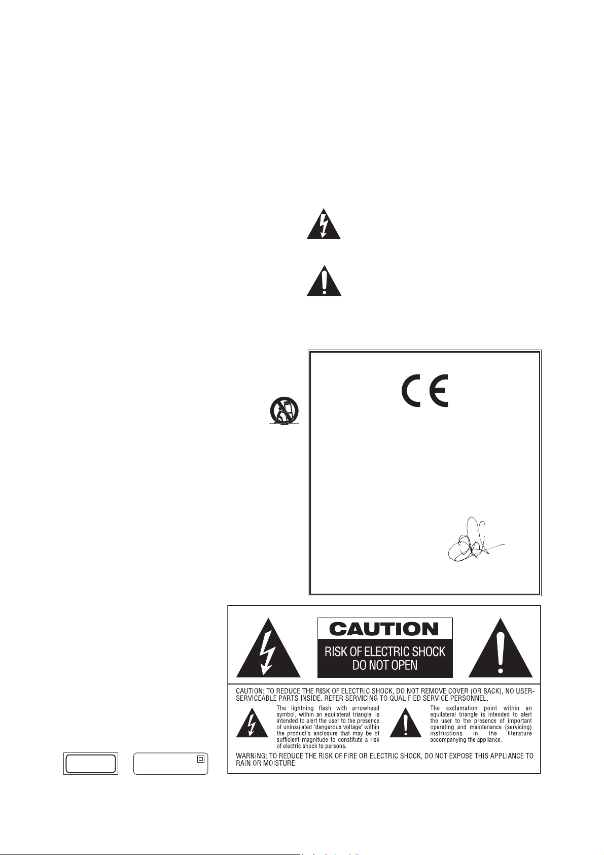
The lightning flash with arrowhead symbol, within an equilateral
triangle, is intended to alert the user to the presence of
uninsulated “dangerous voltage” within the product’s enclosure
The exclamation point within an equilateral triangle is intended
to alert the user to the presence of important operating and
maintenance (servicing) instructions in the literature
Declaration of Conformity
We, Harman Consumer Group, Inc.
2, Route de Tours
72500 Château-du-Loir,
FRANCE
Jurjen Amsterdam
Harman Consumer Group, Inc.
02/09
CLASS 1
LASER PRODUCT
2
Class II equipment symbol
This symbol indicates that the unit has
a double insulation system
for BDP10
Page 5

5
harman/kardon BDP 1 / BDP 10 Service Manual
SAFETY INFORMATION
for BDP10
Important Safety Information
Verify Line Voltage Before Use
Your BDP 10 has been designed for use with 110–240-volt AC current, and the
plug is specifically designed for 230-volt applications. Connection to a line voltage
other than that for which the plug is intended can create a safety and fire hazard
and may damage the unit.
If you have any questions about the voltage requirements for your specific model,
or about the line voltage in your area, contact your selling dealer before plugging
the unit into a wall outlet.
Do Not Use Extension Cords
To avoid safety hazards, use only the power cord attached to your unit. We do not
recommend that extension cords be used with this product. As with all electrical
devices, do not run power cords under rugs or carpets or place heavy objects on
them. Damaged power cords should be replaced immediately by an authorized service
center with a cord meeting factory specifications.
Handle the AC Power Cord Gently
When disconnecting the power cord from an AC outlet, always pull the plug; never
pull the cord. If you do not intend to use the unit for any considerable length of
time, disconnect the plug from the AC outlet.
Do Not Open the Cabinet
There are no user-serviceable components inside this product. Opening the
cabinet may present a shock hazard, and any modification to the product will
void your guarantee. If water or any metal object such as a paper clip, wire or
staple accidentally falls inside the unit, disconnect it from the AC power source
immediately, and consult an authorized service center.
Installation Location
s4OENSUREPROPEROPERATIONANDTOAVOIDTHEPOTENTIALFORSAFETYHAZARDSPLACE
the unit on a firm and level surface. When placing the unit on a shelf, be certain
that the shelf and any mounting hardware can support the weight of the product.
s-AKECERTAINTHATPROPERSPACEISPROVIDEDBOTHABOVEANDBELOWTHEUNITFOR
ventilation. If this product will be installed in a cabinet or other enclosed area,
make certain that there is sufficient air movement within the cabinet. Under
some circumstances, a fan may be required. The unit should be placed on its
own shelf, not directly on top of another component.
s$ONOTPLACETHEUNITDIRECTLYONACARPETEDSURFACE
s!VOIDINSTALLATIONINEXTREMELYHOTORCOLDLOCATIONSORINANAREATHATISEXPOSED
to direct sunlight or heating equipment.
s!VOIDMOISTORHUMIDLOCATIONS
s$ONOTOBSTRUCTTHEVENTILATIONSLOTSONTHEUNITORPLACEOBJECTSDIRECTLYOVER
them.
s $UETOTHEHEATGENERATEDBYOPERATIONOFTHE"$0ANDOTHER
componentsin your system, there is the remote possibility that the rubber
padding on the bottom of the unit’s feet may leave marks on certain wood or
veneer materials. Use caution when placing the unit on soft woods or other
materials that may be damaged by heat or heavy objects. Some surface
finishes may be particularly sensitive to absorbing such marks, due to a variety
of factors beyond Harman Kardon’s control, including the nature of the finish,
cleaning materialsused, and normal heat and vibration caused by the use of
the product, or otherfactors. We recommend that caution be exercised in
choosing an installation location for the component and in normal maintenance
practices, as your warranty will not cover this type of damage to furniture.
Cleaning
When the unit gets dirty, wipe it with a clean, soft, dry cloth. If necessary, and only
after unplugging the AC power cord, wipe it with a soft cloth dampened with mild
soapy water, then a fresh cloth with clean water. Wipe it dry immediately with a dry
cloth. NEVER use benzene, aerosol cleaners, thinner, alcohol or any other volatile
cleaning agent. Do not use abrasive cleaners, as they may damage the finish of
metal parts. Avoid spraying insecticide near the unit.
Moving the Unit
Before moving the unit, be certain to disconnect any interconnection cords with
other components, and make certain that you disconnect the unit from the AC
outlet.
NOTE: To avoid damage to the BDP 10 that may not be covered by the warranty,
remove the disc from the unit before it is moved. Once the BDP 10 is installed,
a disc may be left in the unit when it is turned off, but the unit should NEVER be
moved with a disc left in the disc tray.
Important Information for the User
This equipment has been tested and found to comply with the limits for a Class
B digital device, pursuant to Part 15 of the FCC Rules. The limits are designed
to provide reasonable protection against harmful interference in a residential
installation. This equipment generates, uses and can radiate radio-frequency
energy and, if not installed and used in accordance with the instructions, may
cause harmful interference to radio communication. However, there is no
guarantee that harmful interference will not occur in a particular installation. If this
equipment does cause harmful interference to radio or television reception, which
can be determined by turning the equipment off and on, the user is encouraged to
try to correct the interference by one or more of the following measures:
s2EORIENTORRELOCATETHERECEIVINGANTENNA
s)NCREASETHESEPARATIONBETWEENTHEEQUIPMENTANDRECEIVER
s#ONNECTTHEEQUIPMENTINTOANOUTLETONACIRCUIT
receiver is connected.
s#ONSULTTHEDEALERORANEXPERIENCEDRADIO46TECHNICIANFORHELP
This device complies with Part 15 of the FCC Rules. Operation is subject to the
following two conditions: (1) this device may not cause harmful interference, and
(2) this device must accept interference received, including interference that may
cause undesired operation.
NOTE: Changes or modifications may cause this unit to fail to comply with Part
the FCC Rules and may void the user’s authority to operate the equipment.
CAUTION: The BDP 10 uses a laser system. To prevent direct exposure to the laser
beam, do not open the cabinet enclosure or defeat any of the safety mechanisms
PROVIDEDFORYOURPROTECTION$/./434!2%).4/4(%,!3%2"%!-4OENSUREPROPER
USEOFTHISPRODUCTPLEASEREADTHIS/WNERS-ANUALCAREFULLYANDRETAINITFORFUTUREUSE
Should the unit require maintenance or repair, please contact your local Harman Kardon
service center. Refer servicing to qualified personnel only.
different from that to which the
15 of
Unpacking
The carton and shipping materials used to protect your new player during shipment
were specially designed to cushion it from shock and vibration. We suggest that
you save the carton and packing materials for use in shipping if you move, or
should the unit ever need repair.
To minimize the size of the carton in storage, you may wish to flatten it. This is
done by carefully slitting the tape seams on the bottom and collapsing the carton. Other
cardboard inserts may be stored in the same manner. Packing materials that cannot be
collapsed should be saved along with the carton in a plastic bag.
If you do not wish to save the packaging materials, please note that the carton
and other sections of the shipping protection are recyclable. Please
environment and discard those materials at a local recycling center.
It is important that you remove the protective plastic film from the front-panel lens.
Leaving the film in place will affect the performance of your remote control.
respect the
for BDP10
ENGLISH
3
Page 6
6
harman/kardon BDP 1 / BDP 10 Service Manual
SAFETY INFORMATION
Important Safety Instructions
1. Read these instructions.
2. Keep these instructions.
3. Heed all warnings.
4. Follow all instructions.
5. Do not use this apparatus near water.
6. Clean only with a dry cloth.
7. Do not block any ventilation openings. Install in accordance with the
manufacturer’s instructions.
8. Do not install near any heat sources such as radiators, heat registers, stoves or
other apparatus (including amplifiers) that produce heat.
9. Do not defeat the safety purpose of the polarized or grounding-type plug. A
polarized plug has two blades with one wider than the other. A grounding-type
plug has two blades and a third grounding prong. The wide blade or the third
prong is provided for your safety. If the provided plug does not fit into your
outlet, consult an electrician for replacement of the obsolete outlet.
10. Protect the power cord from being walked on or pinched, particularly at plugs,
convenience receptacles and the point where they exit from the apparatus.
11. Only use attachments/accessories specified by the manufacturer.
12. Use only with the cart, stand, tripod, bracket or table specified by
the manufacturer or sold with the apparatus. When a cart is used,
use caution when moving the cart/apparatus combination to avoid
injury from tip-over.
13. Unplug this apparatus during lightning storms or when unused for long periods
of time.
14. Refer all servicing to qualified service personnel. Servicing is required when the
apparatus has been damaged in any way, such as power supply cord or plug is
damaged, liquid has been spilled or objects have fallen into the apparatus, the
apparatus has been exposed to rain or moisture, does not operate normally, or
has been dropped.
15. Do not expose this apparatus to dripping or splashing and ensure that no
objects filled with liquids, such as vases, are placed on the apparatus.
16. To completely disconnect this apparatus from the AC Mains, disconnect the
power supply cord plug from the AC receptacle.
17. The mains plug of the power supply cord shall remain readily operable.
18. Do not expose batteries to excessive heat such as sunshine, fire or the like.
for BDP1
The lightning flash with arrowhead symbol, within an equilateral
triangle, is intended to alert the user to the presence of uninsulated
“dangerous voltage” within the product’s enclosure that may be of
sufficient magnitude to constitute a risk of electric shock to persons.
The exclamation point within an equilateral triangle is intended to alert
the user to the presence of important operating and maintenance
(servicing) instructions in the literature accompanying the product.
WARNING: To reduce the risk of fire or electric shock, do not expose this apparatus
to rain or moisture.
2
Page 7

7
harman/kardon BDP 1 / BDP 10 Service Manual
SAFETY INFORMATION
Important Safety Information
Verify Line Voltage Before Use
Your BDP 1 has been designed for use with 110–240-volt AC current, and the
plug is specifically designed for 120-volt applications. Connection to a line voltage
other than that for which the plug is intended can create a safety and fire hazard
and may damage the unit.
If you have any questions about the voltage requirements for your specific model,
or about the line voltage in your area, contact your selling dealer before plugging
the unit into a wall outlet.
Do Not Use Extension Cords
To avoid safety hazards, use only the power cord attached to your unit. We do not
recommend that extension cords be used with this product. As with all electrical
devices, do not run power cords under rugs or carpets or place heavy objects on
them. Damaged power cords should be replaced immediately by an authorized service
center with a cord meeting factory specifications.
Handle the AC Power Cord Gently
When disconnecting the power cord from an AC outlet, always pull the plug; never
pull the cord. If you do not intend to use the unit for any considerable length of time,
disconnect the plug from the AC outlet.
Do Not Open the Cabinet
There are no user-serviceable components inside this product. Opening the cabinet
may present a shock hazard, and any modification to the product will void your
guarantee. If water or any metal object such as a paper clip, wire or staple accidentally
falls inside the unit, disconnect it from the AC power source immediately, and consult
an authorized service center.
Installation Location
• To ensure proper operation and to avoid the potential for safety hazards, place
the unit on a firm and level surface. When placing the unit on a shelf, be certain
that the shelf and any mounting hardware can support the weight of the product.
• Make certain that proper space is provided both above and below the unit for
ventilation. If this product will be installed in a cabinet or other enclosed area,
make certain that there is sufficient air movement within the cabinet. Under some
circumstances, a fan may be required. The unit should be placed on its own shelf,
not directly on top of another component.
• Do not place the unit directly on a carpeted surface.
• Avoid installation in extremely hot or cold locations, or in an area that is exposed
to direct sunlight or heating equipment.
• Avoid moist or humid locations.
• Do not obstruct the ventilation slots on the unit, or place objects directly
over them.
• Due to the heat generated by operation of the BDP 1 and other components
in your system, there is the remote possibility that the rubber padding on
the bottom of the unit’s feet may leave marks on certain wood or veneer
materials. Use caution when placing the unit on soft woods or other materials
that may be damaged by heat or heavy objects. Some surface finishes may be
particularly sensitive to absorbing such marks, due to a variety of factors beyond
Harman Kardon’s control, including the nature of the finish, cleaning materials
used, and normal heat and vibration caused by the use of the product, or other
factors. We recommend that caution be exercised in choosing an installation
location for the component and in normal maintenance practices, as your
warranty will not cover this type of damage to furniture.
Cleaning
When the unit gets dirty, wipe it with a clean, soft, dry cloth. If necessary, and only after
unplugging the AC power cord, wipe it with a soft cloth dampened with mild soapy
for BDP1
water, then a fresh cloth with clean water. Wipe it dry immediately with a dry cloth.
NEVER use benzene, aerosol cleaners, thinner, alcohol or any other volatile cleaning
agent. Do not use abrasive cleaners, as they may damage the finish of metal parts.
Avoid spraying insecticide near the unit.
Moving the Unit
Before moving the unit, be certain to disconnect any interconnection cords with other
components, and make certain that you disconnect the unit from the AC outlet.
NOTE: To avoid damage to the BDP 1 that may not be covered by the warranty,
remove the disc from the unit before it is moved. Once the BDP 1 is installed, a disc
may be left in the unit when it is turned off, but the unit should NEVER be moved
with a disc left in the disc tray.
Important Information for the User
This equipment has been tested and found to comply with the limits for a Class B
digital device, pursuant to Part 15 of the FCC Rules. The limits are designed to
provide reasonable protection against harmful interference in a residential installation.
This equipment generates,
installed and used in accordance with the instructions, may cause harmful interference
to radio communication. However, there is no guarantee that harmful interference will
not occur in a particular installation. If this equipment does cause harmful interference
to radio or television reception, which can be determined by turning the equipment
off and on, the user is encouraged to try to correct the interference by one or more
of the following measures:
• Reorient or relocate the receiving antenna.
• Increase the separation between the equipment and receiver.
• Connect the equipment into an outlet on a circuit
receiver is connected.
• Consult the dealer or an experienced radio/TV technician for help.
This device complies with Part 15 of the FCC Rules. Operation is subject to the
following two conditions: (1) this device may not cause harmful interference, and
(2) this device must accept interference received, including interference that may
cause undesired operation.
NOTE: Changes or modifications may cause this unit to fail to comply with Part
the FCC Rules and may void the user’s authority to operate the equipment.
CAUTION: The BDP 1 uses a laser system. To prevent direct exposure to the laser beam,
do not open the cabinet enclosure or defeat any of the safety mechanisms provided for
your protection. DO NOT STARE INTO THE LASER BEAM. To ensure proper use of this
product, please read this Owner’s Manual carefully and retain it for future use. Should the
unit require maintenance or repair, please contact your local Harman Kardon service center.
Refer servicing to qualified personnel only.
uses and can radiate radio- frequency energy
different from that to which the
and, if not
15 of
Unpacking
The carton and shipping materials used to protect your new player during shipment
were specially designed to cushion it from shock and vibration. We suggest that you
save the carton and packing materials for use in shipping if you move, or should the
unit ever need repair.
To minimize the size of the carton in storage, you may wish to flatten it. This is
done by carefully slitting the tape seams on the bottom and collapsing the carton. Other
cardboard inserts may be stored in the same manner. Packing materials that cannot be
collapsed should be saved along with the carton in a plastic bag.
If you do not wish to save the packaging materials, please note that the carton
and other sections of the shipping protection are recyclable. Please
environment and discard those materials at a local recycling center.
It is important that you remove the protective plastic film from the front-panel lens.
Leaving the film in place will affect the performance of your remote control.
respect the
ENGLISH
3
Page 8
8
harman/kardon BDP 1 / BDP 10 Service Manual
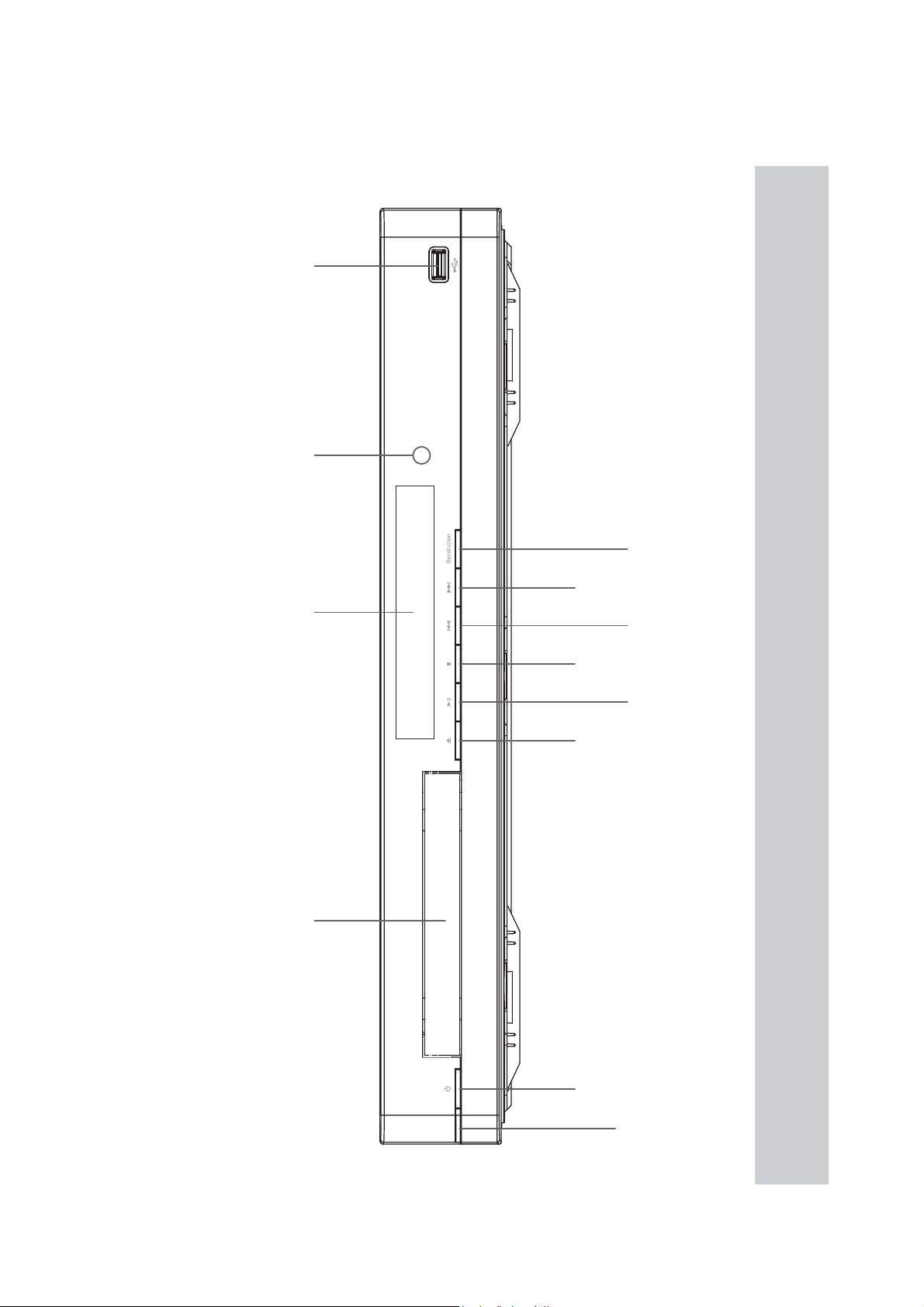
FRONT-PANEL CONTROLS
USB PortRemote IR Sensor-ESSAGE$ISPLAYDIsc Drawer
Forward
Skip/Step
Stop
Open / ClosePower
Resolution
Video Output
Skip /
Reverse
Play / Pause
PowerIndicator
NOTE: To make it easier to follow the instructions throughout the manual that refer to this illustration, a copy of this page may be downloaded from the Product Support section at
www.harmankardon.com.
Page 9

9
harman/kardon BDP 1 / BDP 10 Service Manual
FRONT-PANEL CONTROLS
Power Indicator: Turns amber when the BDP 10 is plugged in and
THEREARPANEL-ASTER0OWER3WITCHISTURNEDONINDICATINGTHATTHE
BDP 10 is in Standby mode and may be turned on using either the
front-panel or remote Power switch. Turns white when the BDP 10 is
turned on.
Power: Press to turn on the BDP 10, when it is connected to an AC
POWERSOURCEANDTHEREARPANEL-ASTER0OWER3WITCHISON
Disc Drawer: Holds the discs to be played. Carefully seat all discs in
the recess in the tray. To avoid damaging the drawer, do not press
down on it when open.
Message Display: Various status messages appear in the text display.
When content is playing, the track and chapter information and the
running time appear. Other indicators will light to display the current
playback mode, video settings or other aspects of the BDP 10’s
status. See page 10 for details.
Open/Close: Press to open or close the disc drawer.
t
II
Play/Pause (
Q
Stop (
): Press to start, pause or resume playback.
): Press to stop playback. When a video is playing, press it
once for Resume mode, and twice to fully stop playback.
ss
I
Skip Reverse (
): Press once to return to the beginning of the
current chapter or track. Quickly press again to skip to previous
chapters or tracks.
Skip/Step Forward (
tt
I): Each press advances to the next chapter
or track. For frame-by-frame advance (forward only), press the Pause
Button, then tap the Skip/Step Forward Button.
Video Output Resolution: Press to display the current video output
resolution. Each additional press changes to the next setting. Only
settings compatible with the TV and type of video connection will be
available.
Remote IR Sensor: This sensor receives infrared commands from the
REMOTECONTROL-AKESURETHATITISNOTBLOCKED
USB Port: Connect a USB storage device, such as a flash drive or
external hard-disc drive, to play additional content. DO NOT connect
card readers, computers, keyboards, pointing devices or other
peripheral products to the BDP 10. Do not connect an iPod here.
ENGLISH
9
Page 10
10
harman/kardon BDP 1 / BDP 10 Service Manual
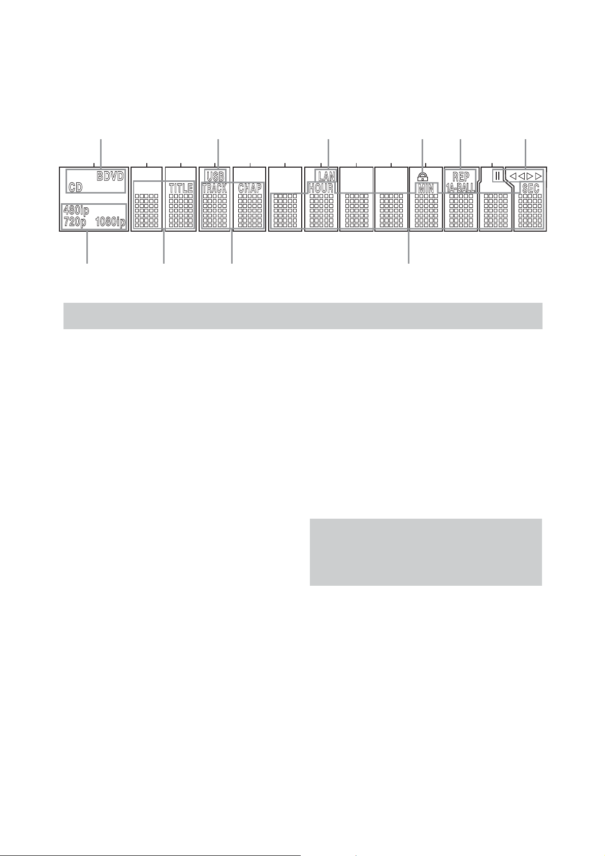
MESSAGE DISPLAY
Disc Type USB Network ParentalLock Repeat 0LAYBACK-ODE
TimeTrack / ChapterTitleVideo OutputResolution
NOTE: To make it easier to follow the instructions that refer to the controls and connectors in this illustration, a larger copy may be
downloaded from the Product Support section for this product at www.harmankardon.com.
Disc Type: Indicates the current disc as BD (Blu-ray Disc), DVD or
CD.
USB: Lights when a USB drive is selected as the playback source.
Network: This indicator lights when the RJ45 jack is connected to a
live network.
Parental Lock: Lights in red when the parental-lock system is active.
Repeat: These indicators light when any of the Repeat functions are in
use.
Playback Mode: These indicators light to show the current playback
mode:
t
Lights when content is playing in the Normal or Slow Play mode.
tt
Lights in the Fast Search Forward mode, with the speed shown on
screen.
II Lights when the disc is paused.
ss
Lights when the disc is in the Fast Search Reverse mode, with the
speed shown on screen.
Time: These positions show the running time of the current media.
Track/Chapter: When a video disc is playing, these two positions
show the current chapter. When a CD is playing, they will show the
current track number.
Title: These two positions show the current title number when a video
disc is playing.
Video Output Resolution: Indicates the current video output
RESOLUTION&ORTHE($-)/UTPUTTHERESOLUTIONISSETAUTOMATICALLYTO
the maximum capability of the TV, but may be changed to a lower
setting. For the Component Video Output, it must be adjusted manually
by pressing the front-panel Video Output Resolution Button, and it may
be set lower than the TV’s maximum capability. When the Composite
Video Output is in use, this indicator will always default to 576i/480i
(interlaced scan), and cannot be changed.
NOTE4HEIIRESOLUTIONISNOTAVAILABLEVIATHE($-)
/UTPUT)FTHE($-)/UTPUTISCONNECTEDSIMULTANEOUSLYWITH
THE#OMPOSITE6IDEO/UTPUTTHISINDICATORWILLREFLECTTHE($-)
Output’s resolution, and the signal at the Composite Video Output
will remain at 576i/480i.
Page 11
11
harman/kardon BDP 1 / BDP 10 Service Manual
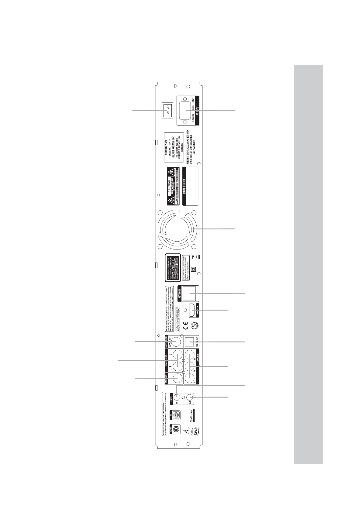
REAR-PANEL CONNECTIONS
for BDP10
-ASTER0OWER3WITCH
AC Power Input
ENGLISH
Fan Vents
Outputs
Analog Audio
Audio Output
Coaxial Digital
Output
Composite Video
Network Jack
($-)/UTPUT
Output
Optical DigitalAudio
Outputs
Component Video
Input
Remote IR
Output
Remote IR
NOTE: To make it easier to follow the instructions throughout the manual that refer to this illustration, a copy of this page may be downloaded from the Product Support section at
www.harmankardon.com.
Page 12

12
harman/kardon BDP 1 / BDP 10 Service Manual
REAR-PANEL CONNECTIONS
Remote Infrared (IR) Input and Output: When the front-panel
Remote IR sensor is blocked, connect the IR Output of your receiver/
processor or an optional IR receiver to the Remote IR Input jack. The
Remote IR Output may be connected to the Remote IR Input of a
compatible product for remote control through the BDP 10. When
several devices are used, connect them in “daisy chain” fashion.
Composite Video Output:)FYOURVIDEODISPLAYDOESNOTHAVE($-)
or component video inputs, connect this video output to your A/ V
receiver/processor or directly to the display.
Component Video Outputs: If your A/ V receiver, surround processor
ORVIDEODISPLAYISNOTEQUIPPEDFOR($-)OR$6)CONNECTTHESEJACKS
to the corresponding inputs on the receiver or TV. If your video display
has component input jacks marked “High Definition,” use those jacks.
Analog Audio Outputs:)FYOUARENOTUSINGEITHER($-)ORASEPARATE
optical or coaxial digital audio connection, connect these jacks to the
A/V receiver or TV. Connect these jacks in addition to a digital audio
connection to make recordings for personal use, or for a multizone
system.
Coaxial and Optical Digital Audio Outputs: If your A/ V receiver
or surround processor is not capable of processing the audio from an
($-)STREAMCONNECTEITHEROFTHESEDIGITALAUDIOOUTPUTSBUTNOT
both) to the receiver/processor.
HDMI Output:#ONNECTTOAN($-)COMPATIBLE! 6RECEIVERORVIDEO
display device. If your A/ V receiver or surround processor is capable of
DECODINGAUDIOFROMTHE($-)STREAMNOFURTHERAUDIOCONNECTIONIS
needed.
NOTE: If your A/V receiver or video display uses DVI connections,
USEANOPTIONAL($-)TO$6)ADAPTERORCABLEANDMAKEA
separate audio connection. If your DVI-equipped display is not
HDCP-compliant, you must use an analog video connection.
Network Jack: Connect this standard RJ45 jack to a broadband
network (Ethernet) connection so that you may take full advantage
of BD-Live updates, features and enhancements of the BonusView
system. When the network connection is “live,” the lights on either side
of the jack will flash to indicate network activity.
NOTE: When the BDP 10 is used with an IP-based or wireless
control device, connect a router/access point here, making certain
that one connection runs from the router to a broadband Internet
connection.
Master Power Switch: Flip on to apply power to the BDP 10,
placing it in the Standby mode. When the unit will not be used for an
extended period of time, or whenever it is necessary to remove the
unit from the AC power lines, flip the switch off.
AC Power Input: Connect the supplied AC power cord to this socket
first, and then to an unswitched AC outlet. Should the cord become
damaged, contact your authorized Harman Kardon dealer for a
replacement.
for BDP10
Fan Vents: This area contains vents used by the BDP 10’s fan to cool
THESYSTEM-AINTAINACLEARANCEOFATLEASTINCHESTOTHENEAREST
surface, to avoid overheating the unit.
12
Page 13
13
harman/kardon BDP 1 / BDP 10 Service Manual
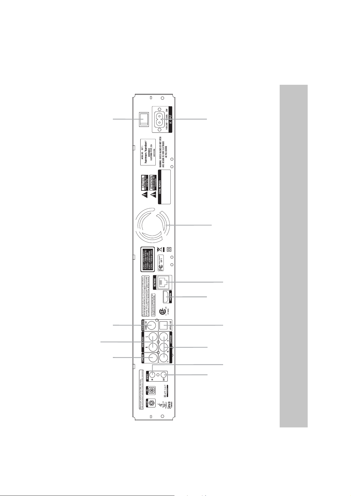
REAR-PANEL CONNECTIONS
for BDP1
Master Power
Switch
ON OFF
AC Power
Input
ENGLISH
Fan Vents
Coaxial Digital
Audio Output
Analog Audio
Outputs
Composite
Video Output
HDMI
Output
Component
Video Outputs
Remote
IR Output
Network Jack
Optical Digital
Audio Output
Remote
IR Input
www.harmankardon.com.
NOTE: To make it easier to follow the instructions throughout the manual that refer to this illustration, a copy of this page may be downloaded from the Product Support section at
Page 14

14
harman/kardon BDP 1 / BDP 10 Service Manual
REAR-PANEL CONNECTIONS
Remote Infrared (IR) Input and Output: When the front-panel Remote
IR sensor is blocked, connect the IR Output of your receiver/processor
or an optional IR receiver to the Remote IR Input jack. The Remote IR
Output may be connected to the Remote IR Input of a compatible
product for remote control through the BDP 1. When several devices
are used, connect them in “daisy chain” fashion.
Composite Video Output: If your video display does not have HDMI
or component video inputs, connect this video output to your A/ V
receiver/processor or directly to the display.
Component Video Outputs: If your A/V receiver, surround processor
or video display is not equipped for HDMI or DVI, connect these jacks
to the corresponding inputs on the receiver or TV. If your video display
has component input jacks marked “High Definition,” use those jacks.
Analog Audio Outputs: If you are not using either HDMI or a separate
optical or coaxial digital audio connection, connect these jacks to the
A/V receiver or TV. Connect these jacks in addition to a digital audio
connection to make recordings for personal use, or for a multizone
system.
Coaxial and Optical Digital Audio Outputs: If your A/V receiver or
surround processor is not capable of processing the audio from an HDMI
stream, connect either of these digital audio outputs (but not both) to
the receiver/processor.
HDMI Output: Connect to an HDMI-compatible A/ V receiver or video
display device. If your A/V receiver or surround processor is capable
of decoding audio from the HDMI stream, no further audio connection
is needed.
NOTE: If your A/V receiver or video display uses DVI connections,
use an optional HDMI-to-DVI adapter or cable, and make a
separate audio connection. If your DVI-equipped display is not
HDCP-compliant, you must use an analog video connection.
Network Jack: Connect this standard RJ45 jack to a broadband
network (Ethernet) connection so that you may take full advantage of
BD-Live updates, features and enhancements of the BonusView system.
When the network connection is “live,” the lights on either side of the
jack will flash to indicate network activity.
NOTE: When the BDP 1 is used with an IP-based or wireless
control device, connect a router/access point here, making
certain that one connection runs from the router to a broadband
Internet connection.
Master Power Switch: Flip on to apply power to the BDP 1, placing
it in the Standby mode. When the unit will not be used for an extended
period of time, or whenever it is necessary to remove the unit from the
AC power lines, flip the switch off.
AC Power Input: Connect the supplied AC power cord to this socket
first, and then to an unswitched AC outlet. Should the cord become
damaged, contact your authorized Harman Kardon dealer for a
replacement.
for BDP1
Fan Vents: This area contains vents used by the BDP 1’s fan to cool
the system. Maintain a clearance of at least 3 inches to the nearest
surface, to avoid overheating the unit.
12
Page 15
15
harman/kardon BDP 1 / BDP 10 Service Manual
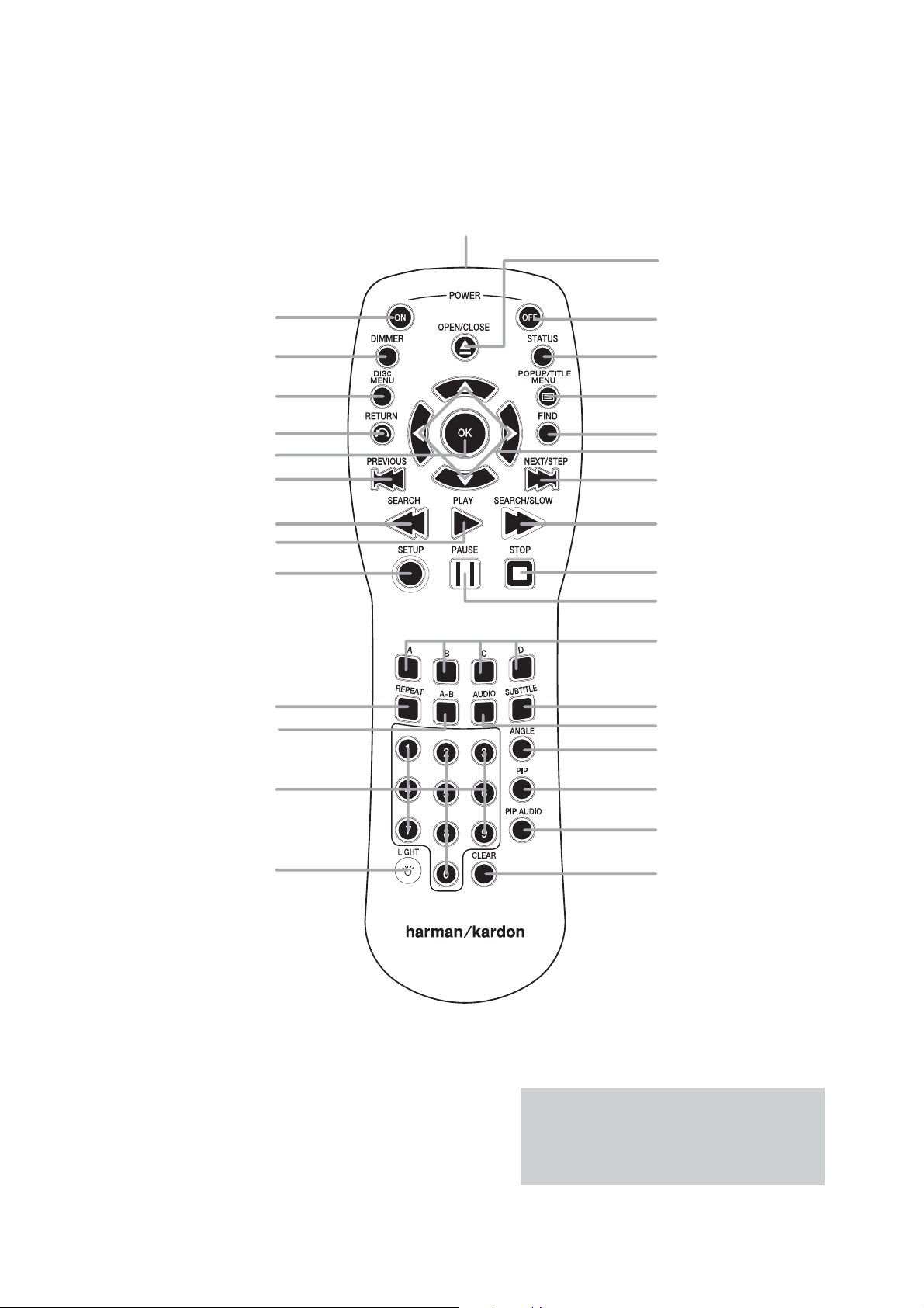
REMOTE CONTROL FUNCTIONS
IR Transmitter Lens
Open/Close
Power On
Dimmer
$ISC-ENU
Return
Previous
Search Reverse
Play
Setup
Repeat
A-B Repeat
Power Off
Status
ENGLISH
0OPUP4ITLE-ENU
Find
q/r
OK
/s/t Navigation
Next/Step
Search/Slow Forward
Stop
Pause
Soft Keys
Subtitle
Audio
Angle
Numeric Keys
Backlight
PIP
PIP Audio
Clear
NOTE: To make it easier to follow the instructions
throughout the manual that refer to this illustration, a
copy of this page may be downloaded from the Product
Support section at www.harmankardon.com.
Page 16

16
harman/kardon BDP 1 / BDP 10 Service Manual
REMOTE CONTROL FUNCTIONS
IR Transmitter Lens: When buttons are pressed on the remote,
INFRAREDCODESAREEMITTEDTHROUGHTHISLENS-AKESUREITISPOINTING
toward the BDP 10.
Power On: Press to turn on the BDP 10 when it is in the Standby
mode.
Power Off: Press to turn off the BDP 10, placing it in the Standby
mode.
Open/Close: Press to open or close the disc drawer.
Dimmer: Press to change the front-panel display to half- or full-
brightness, or to turn it off. When the indicators are fully dimmed, the
Power Indicator will remain lit to remind you that the unit is on. Press
any button to temporarily return the front panel to full-brightness.
Status: Press during playback to display the current title and chapter
or track.
Disc Menu: Press to view a disc’s main menu. Playback will pause.
Popup/Title Menu: Press while a BD-Video disc is playing to display
a menu bar at the bottom of the screen or elsewhere, depending
on the disc. This is one of the Blu-ray Disc system’s most exciting
innovations, as video playback will continue while you access the
disc’s setup, scene selection and special features submenus and make
ADJUSTMENTSONTHEFLY)FYOUSELECTh$ISC-ENUvPLAYWILLSTOPANDTHE
main disc menu will appear. Depending on the disc, other functions
may be implemented as popup menus during playback.
q/r
Navigation
on-screen menus. When still images are displayed, use the
Buttons to scroll through the images in the folder.
OK Button: Press to enter a menu selection.
Return: Press to return to the previous menu or menu selection level.
Find: While a disc is playing, press to jump to a different location
on the disc. Each press changes the search mode: Title, Chapter or
Time. Use the Numeric Keys to specify the location, and press the OK
Button.
Previous: Press once to return to the start of the current chapter or
track. Press it again to step through previous chapters or tracks.
(
t
/s/
): These buttons are used to navigate the
s/t
Pause: Press to momentarily pause playback. Press again to resume.
While paused, press the Next Step Button for frame-by-frame
advance, or press the Search Forward Button for slow-motion play.
Stop: When audio content is playing, press to stop playback. When a
BD or DVD disc is playing, press once to place the unit in the Resume
mode, where pressing the Play button will resume playback from the
place where it stopped. Press the Stop Button twice when a BD or
DVD disc is playing to bring the unit to a “full stop.”
Soft Keys: These four color-coded buttons are used for Blu-ray Disc
special features, and are defined by the disc.
Repeat: Press to repeat the current title or chapter while a DVD disc
is playing, or to repeat the current track or all tracks on an audio CD.
Each press changes the Repeat mode, or turns off Repeat play. To
repeat content on a data disc or USB drive, first create a playlist. See
pages 23 to 24 for more information.
A-B Repeat: Press to select a passage for repeat play. The first press
determines the beginning of the passage, the second press defines
the end point and the third press cancels A-B Repeat play. The A-B
Repeat function is only available for some Blu-ray Disc media.
Audio: Press to select from the available audio format and/or language
options.
Subtitle: Press to select from the available subtitle language options.
Angle: When a BD or DVD disc is playing and multiple-angle content
is available (as indicated on screen), press this button to toggle through
the available views.
PIP: Press to switch to a secondary video stream while playing a
BD-Video disc with BonusView special features.
PIP Audio: Press to switch to a secondary audio track while playing a
BD-Video disc with BonusView special features.
Numeric Keys: Press these buttons to enter numeric data.
Backlight: Press to activate the remote’s backlighting system.
Clear: Press to clear menus from the on-screen display, or to cancel
alphanumeric entries.
Next/Step: When content is playing, each press advances to the
next chapter or track. When video content is playing, press the Pause
Button first, then each press of this button advances the video one
frame. The Step function is not available in reverse.
Search Reverse: Press to scan backward through the current
program. Each press changes the speed: 2x, 4x, 8x, 16x, 32x, 64x or
128x. The slow-motion function is not available in reverse.
Play: Press to begin playback.
Search/Slow Forward: Press to scan forward through the current
program. Each press changes the speed: 2x, 4x, 8x, 16x, 32x, 64x
or 128x. For slow-motion play of video content, press the Pause
Button first, then each press of this button changes the speed: 1/8x,
1/4x or 1/2x.
Setup: Press to configure system options.
14
Page 17

17
harman/kardon BDP 1 / BDP 10 Service Manual
INSTALLATION
for BDP10
IMPORTANT NOTE: All components, including the BDP 10, should
be turned off and unplugged from AC power before beginning
installation. Do not plug any components back in until after all
connections are completed.
Step One – Placement
Other system components, especially audio/video receivers and
amplifiers, generate massive amounts of heat that will damage the
sensitive laser components of the BDP 10. Although the BDP 10 is
equipped with a fan that will turn on occasionally to compensate for
heat conditions, it is strongly recommended that you place the BDP 10
on its own shelf. Do not stack components on top of each other.
Step Two – Connect the BDP 10 to an A/V Receiver
or Processor (Preferred)
)FTHERECEIVERIS($-)CAPABLECONNECTTHE($-)/UTPUTTOTHE
RECEIVERS($-)INPUT3EE&IGURE
&IGUREn($-)/UTPUT
)FTHERECEIVERHASA$6)INPUTANDIS($#0COMPLIANTUSEAN($-)
to-DVI adapter, and make a separate audio connection.
)FTHERECEIVERDOESNOTHAVEAN($-)OR$6)INPUTSELECTONEVIDEO
connection, in order of preference: component video or composite
video. See Figure 2.
Figure 4 – Analog Audio Outputs
Skip to Step Four.
Step Three – Connect the BDP 10 Directly to a
Television (Alternate)
If an A/ V receiver or processor was used, you may skip this step, or
you may make a second connection from the BDP 10 directly to the
TV to bypass the home theater system for casual viewing. If you do
not have an audio system, connect the BDP 10 to the TV as explained
below.
)FTHETELEVISIONIS($-)CAPABLECONNECTTHE($-)/UTPUTTOTHE46S
($-)INPUT3EE&IGURE
)FTHE46HASONLYA$6)INPUTANDIS($#0COMPLIANTUSEAN($-)
to-DVI adapter, and make a separate audio connection.
)FTHETELEVISIONDOESNOTHAVEAN($-)OR$6)INPUTSELECTONEVIDEO
connection, in order of preference: component video or composite
video. See Figure 2.
&ORNON($-)46SASEPARATEAUDIOCONNECTIONISREQUIRED!LTHOUGH
some TVs may be equipped with an optical or coaxial digital audio
connection, most likely you will use a 2-channel analog connection.
Connect the Analog Audio Outputs shown in Figure 4 to the TV.
Step Four – Connect a USB Storage Device
Connect a compatible USB client device to the front-panel USB port.
The USB drive may be used as virtual memory for the BD-Live system,
or as a playback source. See Figure 5 and page 22.
ENGLISH
Figure 2 – Component and Composite Video Outputs
&ORNON($-)PRODUCTSASEPARATEAUDIOCONNECTIONISREQUIRED)F
available, connect either the Optical or Coaxial Digital Audio Output to
the receiver. See Figure 3.
Figure 3 – Coaxial and Optical Digital Audio Outputs
Connect the Analog Audio Outputs to a receiver that does not have
an available digital audio input. If digital audio connections have been
made to the receiver, make an analog connection for recording,
multizone systems or as a backup. See Figure 4.
Figure 5 – Front-Panel USB Port
Step Five – Connect the Remote IR Input and
Output (Optional)
Connect the BDP 10’s Remote IR Input to the compatible IR output
of another product, or to an IR receiver or controller, such as the
optional Harman Kardon HE 1000. When daisychaining devices to
allow for remote control up and down the chain, connect the Remote
IR Output to the next product’s IR input. See Figure 6. The BDP 10 is
compatible with “stripped carrier” IR signals.
Page 18

18
harman/kardon BDP 1 / BDP 10 Service Manual
INSTALLATION
Figure 6 – Remote IR Input and Output
for BDP10
Step Six – Network Connection
Connect the Network Jack to a router or Ethernet-compatible
controller. See Figure 7. The network connection is used for BD-Live
discs to access the Internet for updates to the disc content and special
features.
Figure 7 – Network Jack
for BDP10
Step Seven – Plug In AC Power
To avoid possible damage from a transient power surge at plug-in,
TURNOFFTHE-ASTER0OWER3WITCH0LUGTHEFEMALEENDOFTHE!#
Power cord into the receptacle (see Figure 8), and the male end into
an unswitched AC outlet.
Point the remote toward the front panel of the BDP 10. The IR receiver
ISLOCATEDIMMEDIATELYTOTHERIGHTOFTHE-ESSAGE$ISPLAY-AKESURE
no objects are blocking the remote’s path. Bright lights, fluorescent
lights and plasma video displays may interfere with the remote’s
functioning. The remote has a range of about 6 m, depending on the
lighting conditions. It may be used at an angle of up to 30 degrees to
either side of the BDP 10.
If the remote seems to operate intermittently, make sure the batteries
have been inserted correctly, or replace both batteries with fresh ones.
&IGUREn-ASTER0OWER3WITCHAND!#0OWER)NPUT
Step Eight – Insert Batteries in Remote
The BDP 10 remote control uses two AA batteries (included).
To remove the battery cover located on the back of the remote, lift
the tab until the latch releases, and lift the battery cover up. Insert the
batteries as shown in Figure 9, observing the correct polarity.
To replace the cover, insert the two small tabs at the top of the cover
into the recesses at the top of the battery compartment, and lower the
cover, pressing the latch at the bottom until it snaps shut.
Figure 9 – Remote Battery Compartment
16
Page 19

19
harman/kardon BDP 1 / BDP 10 Service Manual
INSTALLATION
for BDP1
IMPORTANT NOTE: All components, including the BDP 1,
should be turned off and unplugged from AC power before
beginning installation. Do not plug any components back in
until after all connections are completed.
Step One – Placement
Other system components, especially audio/video receivers and amplifiers,
generate massive amounts of heat that will damage the sensitive laser
components of the BDP 1. Although the BDP 1 is equipped with a fan
that will turn on occasionally to compensate for heat conditions, it is
strongly recommended that you place the BDP 1 on its own shelf.
Do not stack components on top of each other.
Step Two – Connect the BDP 1 to an A/ V
Receiver or Processor (Preferred)
If the receiver is HDMI-capable, connect the HDMI Output to the
receiver’s HDMI input. See Figure 1.
Figure 1– HDMI Output
If the receiver has a DVI input and is HDCP-compliant, use an HDMIto-DVI adapter, and make a separate audio connection.
If the receiver does not have an HDMI or DVI input, select one video
connection, in order of preference: component video or composite
video. See Figure 2.
to the receiver, make an analog connection for recording, multizone
systems or as a backup. See Figure 4.
Figure 4 – Analog Audio Outputs
Skip to Step Four.
ENGLISH
Step Three – Connect the BDP 1 Directly to a
Television (Alternate)
If an A/ V receiver or processor was used, you may skip this step, or
you may make a second connection from the BDP 1 directly to the TV
to bypass the home theater system for casual viewing. If you do not
have an audio system, connect the BDP 1 to the TV as explained below.
If the television is HDMI-capable, connect the HDMI Output to the TV’s
HDMI input. See Figure 1.
If the TV has only a DVI input and is HDCP-compliant, use an HDMIto-DVI adapter, and make a separate audio connection.
If the television does not have an HDMI or DVI input, select one video
connection, in order of preference: component video or composite
video. See Figure 2.
For non-HDMI TVs, a separate audio connection is required. Although
some TVs may be equipped with an optical or coaxial digital audio
connection, most likely you will use a 2-channel analog connection.
Connect the Analog Audio Outputs shown in Figure 4 to the TV.
Figure 2 – Component and Composite Video Outputs
For non-HDMI products, a separate audio connection is required. If
available, connect either the Optical or Coaxial Digital Audio Output
to the receiver. See Figure 3.
Figure 3 – Coaxial and Optical Digital Audio Outputs
Connect the Analog Audio Outputs to a receiver that does not have an
available digital audio input. If digital audio connections have been made
15
Step Four – Connect a USB Storage Device
Connect a compatible USB client device to the front-panel USB port.
The USB drive may be used as virtual memory for the BD-Live system,
or as a playback source. See Figure 5 and page 22.
Figure 5 – Front-Panel USB Port
Step Five – Connect the Remote IR Input
and Output (Optional)
Connect the BDP 1’s Remote IR Input to the compatible IR output of
another product, or to an IR receiver or controller, such as the optional
Harman Kardon HE 1000. When daisychaining devices to allow for
remote control up and down the chain, connect the Remote IR Output
to the next product’s IR input. See Figure 6. The BDP 1 is compatible
with “stripped carrier” IR signals.
15
Page 20

20
harman/kardon BDP 1 / BDP 10 Service Manual
INSTALLATION
for BDP1
for BDP1
Figure 6 – Remote IR Input and Output
Step Six – Network Connection
Connect the Network Jack to a router or Ethernet-compatible controller.
See Figure 7. The network connection is used for BD-Live discs to
access the Internet for updates to the disc content and special features.
Figure 7 – Network Jack
Step Seven – Plug In AC Power
To avoid possible damage from a transient power surge at plug-in, turn
off the Master Power Switch. Plug the female end of the AC Power cord
into the receptacle (see Figure 8), and the male end into an unswitched
AC outlet.
Point the remote toward the front panel of the BDP 1. The IR receiver is
located immediately to the right of the Message Display. Make sure no
objects are blocking the remote’s path. Bright lights, fluorescent lights
and plasma video displays may interfere with the remote’s functioning.
The remote has a range of about 20 feet (6 meters), depending on the
lighting conditions. It may be used at an angle of up to 30 degrees to
either side of the BDP 1.
If the remote seems to operate intermittently, make sure the batteries
have been inserted correctly, or replace both batteries with fresh ones.
Figure 8 – Master Power Switch and AC Power Input
Step Eight – Insert Batteries in Remote
The BDP 1 remote control uses two AA batteries (included).
To remove the battery cover located on the back of the remote, lift the
tab until the latch releases, and lift the battery cover up. To replace the
cover, insert the two small tabs at the top of the cover into the recesses
at the top of the battery compartment, and lower the cover, pressing the
latch at the bottom until it snaps shut.
Insert the batteries as shown in Figure 9, observing the correct polarity.
Figure 9 – Remote Battery Compartment
16
Page 21

21
harman/kardon BDP 1 / BDP 10 Service Manual
4-1
Software upgrade
Preparation to upgrade software
1) Start the CD Burning software and create a new CD
project (Data Disc)
2) Burn the oppointed data onto a blank CDR
A. Procedure for software upgrade:
1) Power on the set and insert the prepared Upgrade
CDR.
2) The set will starts reading disc & response with the
following display TV screen:
Upgrade File DETECTED
Upgrade?
Press Play TO START.
3) Press <OK> button to confirm, then screen will display :
Files coping…
UPGRADING…
4) The upgraded tray will automatically open when files
coping complete, then take out the disc.
5) About 1 minute later, the trace will automatically close
when upgrading complete.
*
B. Read out the software versions to confirm upgrading
1) Power on the set and press <Setup> button on the
remote control.
2) Then press down cursor on the remote control to choose
"System" , and press the right cursor on the remote control
to choose "software version".
The software version and other information are displayed
on the TV screen as follows:
Version information
CFE Version:X.XX.XX
APP Version:BDP_XX_VX.XX
LOADER Version:XXXX
FP MCU Version:HarmanXX_XXX
* The other upgrade SW way is by memory, the steps are the
same as CDR's, create the upgrade file into memory, and
connect the USB flash drive to the USB socket on set, then
press "USB" on remote control to access the content and
play the upgrade file as above upgrade procedure.
6) Restart the set after above steps;
Remark: If the upgraded software
shows an error message:
A. Same version: Upgrade software twice.
B. Different version: Upgrade the software versions one after
the other, and make sure to upgrade the current version first.
Caution: The set
MUST NOT be powered off
during upgrading, otherwise the Main Board
will be irreparably damaged.
Page 22

harman/kardon BDP 1 / BDP 10 Service Manual
22
Packaging/accessories
Item Description Part Number Qty
1 Outer Carton BDP1 76-982790-0ATB2 1
Outer Carton BDP10 76-982790-0ATB1 1
2 Front Protector 1
3 Plastic Bag 1
4 BDP1 BDP 1 1
BDP10 BDP 10 1
5 Foam End, Right 1
6 Corner Protectors 4
7 Corner Protectors 4
8 HDMI cable 46-HDI015-19G 1
3-conductor analog audio/video cable 41-UH1500-0KKCD 1
AC power cord BDP1 51-BC0150-0LSA9-M 1
AC power cord BDP10 51-DC0150-0CRA4 1
9 Owner’s Manual BDP1 or BDP10 Visit www.harmankardon.com 1
10 Plastic Bag 1
11 Remote control BDP1 or BDP10 RB17H00 or 06-RB17H0-00X 1
AA Batteries 2
12 Foam End, Left 1
Page 23

23
harman/kardon BDP 1 / BDP 10 Service Manual
Exploded View for BDP10 & BDP1:
It's a general mechanical exploded view for BDP10 & BDP1, please refer to
the model set for detailed information.
ASSY 1 includes components:3.7.25.26.28.30.31
Page 24

24
harman/kardon BDP 1 / BDP 10 Service Manual
Please note: Loader 05-BLURAY-BP04 is used last in serial number TL0001-09181.
New loader 05-BLURAY-BP06 is used first in serial number TL-0001-09182.
PARTS LIST: BDP10
Location No. TCL P/N. Description Q'ty
8 08-00BDP1-FB0
12 08-00BDP1-IR0
20 08-00BDP1-MA0
27 08-00BDP1-SW0
21 08-0BDP10-PW0
ASSY1 02-BDP1F1-XXOB2
1.2 08-00BDP1-XXO
22 05-BLURAY-BP04 LOADER BP-04 (later changed, see below 1
AVCABLE 41-UH1500-0KKCD AUDIO/VIDEO CABLE[LOW CADMIUM] 1500m
- 46-SATA03-XXX SATA POWER CORD 1
- 46-SATA10-XXX SATA SIGNAL CORD 15CM 1
POWERCORD 51-DC0150-0CRA4 EUROPEAN POWER CORD 1.5m 1
34 54-981610-000 RUBBER PAD 4
14 67-BDP1B1-1E0B2 BACK PANEL 1
35 67-BDP1R1-1E0B1 BOTTOM PLATE 1
17 67-BDP1T1-0E0B1 TOP COVER 1
IFU 72-0BDP10-120B1 USER MANUAL 1
DBOX 76-982790-0ATB1 DISPLAY BOX 1
CABLE 46-KS006T-03FG 2PIN CABLE 1
13 43-FS512S-214 DC FAN 1
HDMICABLE 46-HDI015-19G HDMI GILDED LINE 1.5M 1
RC 06-RB17H0-00X HARMAN REMOTE CONTROL 1
- 57-BDWDF1-000 LOADER BUCKLE 1
- 67-H97889-1A9 HEATSINK 1
- 48-POW036-XX0 POWER SWITCH 1
1 67-981640-0A0 LOGO 1
ASSY-FB BD
ASSY-IR BD
ASSY-MAIN BD
ASSY-SW BD
ASSY-PW BD
ASSY-FRONT PANEL
ASSY-DECORATIVE ALUMINIUM-BAR
m 1
1
1
1
1
1
1
1
SAFETY PRECAUTION
The parts identified by mark are critical for safety. Replace only with part
number
specified. The mounting position of replacement is to be identical with originals.
The substitute replacement parts which do not have the same safety characteristics
as specified in the parts list may create shock, fire or other hazards.
Page 25

25
harman/kardon BDP 1 / BDP 10 Service Manual
Please note: Loader 05-BLURAY-BP04 is used last in serial number TL0001-09181.
New loader 05-BLURAY-BP06 is used first in serial number TL-0001-09182.
PARTS LIST: BDP1
Location No. TCL P/N. Description Q'ty
8 08-00BDP1-FB0
12 08-00BDP1-IR0
20 08-00BDP1-MA1
27 08-00BDP1-SW0
21 08-00BDP1-PW0
ASSY1 02-BDP1F1-XXOB1
1.2 08-00BDP1-XXO
22 05-BLURAY-BP04 LOADER BP-04 (later changed, see below) 1
AVCABLE 41-UH1500-0KKCD AUDIO/VIDEO CABLE[LOW CADMIUM] 1500m
- 46-SATA03-XXX SATA POWER CORD 1
- 46-SATA10-XXX SATA SIGNAL CORD 15CM 1
POWERCORD 51-BC0150-0LSA9-M POWER CORD 1.5m 1
34 54-981610-000 RUBBER PAD 4
14 67-BDP1B1-1E0B1 BACK PANEL 1
35 67-BDP1R1-1E0B1 BOTTOM PLATE 1
17 67-BDP1T1-0E0B1 TOP COVER 1
IFU visit www.harmankardon.com OWNER'S MANUAL 1
DBOX 76-982790-0ATB2 DISPLAY BOX 1
CABLE 46-KS006T-03FG 2PIN CABLE 1
13 43-FS512S-214 DC FAN 1
HDMICABLE 46-HDI015-19G HDMI GILDED LINE 1.5M 1
RC 06-RB17H0-00X HARMAN REMOTE CONTROL 1
- 57-BDWDF1-000 LOADER BUCKLE 1
- 67-H97889-1A9 HEATSINK 1
- 48-POW036-XX0 POWER SWITCH 1
1 67-981630-0A0 LOGO 1
ASSY-FB BD
ASSY-IR BD
ASSY-MAIN BD
ASSY-SW BD
ASSY-PW BD
ASSY-FRONT PANEL
ASSY-DECORATIVE ALUMINIUM-BAR
1
1
1
1
1
1
1
m 1
SAFETY PRECAUTION
The parts identified by mark are critical for safety. Replace only with part
number
specified. The mounting position of replacement is to be identical with originals.
The substitute replacement parts which do not have the same safety characteristics
as specified in the parts list may create shock, fire or other hazards.
Page 26

26
harman/kardon BDP 1 / BDP 10 Service Manual
Trouble shooting chart
No display on VFD, and buttons do not work
No display on VFD, and
buttons do not work
Yes
Check every supply
voltage on main board is
normal
Yes
No
Check-28V,5V,+12V
voltage on the power
and front board
Yes
Check the front board
signal VDIN,VCLK,
VSTBˈ
No
Fix the connection XP1 on front board
and CN502 on power board
No
Refer to Power supply board part
Check the U3’s pin 45,46,47 singal
Yes
1.Check whether bad solder exists
on U2 and pins of VFD,
2.Check whether the circuit
connected to K7, K2, K3, K4, K5,
K6 is broken.
Yes
Replace U3
No
Correct connection
Page 27

p
27
harman/kardon BDP 1 / BDP 10 Service Manual
Trouble shooting chart
No audio output
No audio output
Go
Check whether the audio signal
is right from the U22 and
U24,U19,U20
Yes
Check whether the audio signal is
right from the U19.1 U19.7 and
U201, U20.7and
uuuU22.1,U22.7,U24.1,U24.7
Yes
Check the connection of
the 12PIN cable from
x
7 on the main board
No
NO
Check the U19,U20, U22,u24
power supply
Ye s
Replace the
U22,U24,U20,U19
NO
Check the U23 power supply
Replace the U23
Connect the 12pin cable
to xp7 properly on output
board
Yes
Replace the output
board
Page 28

28
harman/kardon BDP 1 / BDP 10 Service Manual
Trouble shooting chart
Remote control does not work
Remote control
does not work
Go
Check whether the remote
controller’s battery is
exhausted or not.
NO
Check the IR1 power
supply is vcc,vcc is about
Ye s
5V
Yes
Replace IR1
yes
No
Replace the battery for remote
controller
Check the VCC net no front board
Page 29

29
harman/kardon BDP 1 / BDP 10 Service Manual
Trouble shooting chart
Can’t read disc or can’t open the disk door
Can’t read disc or can’t
open the disk door
GO
Check whether the
DVD loader running is
normal
Yes
Check SATA cable from
main board connection to
the loader is normal
Yes
Replace the loader
NO
Check the connection of the 4PIN cable he
Power Board.
NO
Fix the connection the And SATA cable from
main board
Page 30

30
harman/kardon BDP 1 / BDP 10 Service Manual
Trouble shooting chart
No VFD display
No VFD display
Go
Check whether the voltage
+5Vstb on the front board is
normal work or not.
Yes
Check whether the voltage
between VFD F+&VFD F- is
DC 7V+0.5
Yes
Check whether the
voltage 33 V is normal
No
No
No
Fix the connection power board
CN502 front board XP1
Check DC5V to AC 3V switch circuit
Check the d5 on the front board
Yes
Replace U4,U3
Page 31

31
harman/kardon BDP 1 / BDP 10 Service Manual
Trouble shooting chart
Fan don’t work
Fan don’t work
Go
Check on Power board
whether CN503.1 is
+11V
Yes
Check the cable
connection fan to Power
board CN503
Yes
Replace Fan
No
Check U506.8 on Power board
No
Replace the cable
Page 32

32
harman/kardon BDP 1 / BDP 10 Service Manual
Front Board Print-layout (Top side):
Page 33

33
harman/kardon BDP 1 / BDP 10 Service Manual
Front Board Print-layout (Bottom side):
Page 34

34
harman/kardon BDP 1 / BDP 10 Service Manual
IR Board Print-layout (Bottom side):
Page 35

35
harman/kardon BDP 1 / BDP 10 Service Manual
Power Board Print-layout (Bottom side):
Page 36

36
harman/kardon BDP 1 / BDP 10 Service Manual
Main Board Print-layout (Top side):7-20
Page 37

37
harman/kardon BDP 1 / BDP 10 Service Manual
Main Board Print-layout (Bottom side):
Page 38

38
harman/kardon BDP 1 / BDP 10 Service Manual
Harman BDP 10/BDP 1 Block Diagram
PSU
CN505
4x3.96mm
+5V1GND2GND3+12V
4
1
4
3
+5V
GND2GND
+12V
4x3.96mm
LOADER
SATA
CN502
5 x2.0mm
CN504
+5V STBY
9x2.0mm
+12V
GND
-28V
GND
+5V
PCON
DC in
DC/DC 3.3V
XP1
9x2.0mm
J8
P.11
DC/DC 1.2V
P.11
SATA1
U10
+5V
1
+5V
+5V
2
+5V
GND
3
GND
GND
4
GND
+12V
5
+12V
+12V
6
-12V
GND
7
GND
+5VSTB
8
PCON
9
+12V
5
4
-28V
3
GND
2
+5V
1
Ethernet
J2 J3 J4 J4
USB0 (Header)
XP6
CLOCK
DDR2-0H
P.7
HDMI
Sil9134
7440C
SOC
U3
S/PDIF
TOSLINK
Video buffer
U6
CVBS-L-R
Component
Video buffer
U7
U15
XP5
4PIN,PI CH=2.0
XP4
UARTsBBS
5VSTBY
IR IN
GND
IR OUT
PICH=2.0
JP7
1
2
3
4
NAND
DDR2-0L
P.7
U13
DC/DC 1.8V
P.11
Note: Buses on this drawing represent interchip connections and do not reflect pin or bus location on chip.
U17
U14
IR_LOOP
JP7
J1
main board
U18
DDR2-1H
P.8
DDR2-1L
P.8
XP2
9PIN/2.0mm
DOUT/KEY
VDIN
FPANEL
123456789
㒭䘹༈
ź
REMOTE OUT
POW_SW
3V3-FB
VCLK
GND
VSTB
GND
XP2
CON4
VCC1
4
USB_DP
3
USB_DN
2
GND
1
SWITCH BOARD
5 x2.0mm
XP4
KEY
LED1
LED2
1
2
3
4
PICH=2.0
GND
9PIN/2.0mm
CONS4-L
Page 39

39
harman/kardon BDP 1 / BDP 10 Service Manual
change t o 47UF 0805,add C 0.1UF
2008ׂᬍ .5.19
+1V2
+2V5_BCM7440
21
+3V3
5%
100MW
2.2
R37
+3V3_AUD
12
12
CE8
C582
C580
+
4.7UF
0.1UF
6.3V
470uF/16V
20%
+2V5_BCM7440
100OHMS
L7
+2V5_VDAC
12
C579
4.7UF
12
+3V3_VDAC
12
C578
0.1UF
12
L8
100OHMS
12
C577
22UF
+3V3
Add the 22 uF CAP,change C567 to 0.1UF
+1V8
+1V2
+3V3
+2V5_BCM7440
DDR0_A[13:0]
G1
H3
H4
J5
A3
B3
E4
F4
E8
D9
C9
C8
F6
C7
C5
D5
E5
E7
E15
E14
D15
H15
D14
H14
E11
E12
H11
H13
F12
B15
G16
C15
D17
E17
F17
H17
A15
D16
E16
F16
Y8
Y6
V8
U4
T8
T6
P8
N4
M8
M6
J4
AG6
AG18
AG14
AG10
AE9
AE4
AE17
AE13
AD6
AC17
AC15
AC13
AC11
AA4
Y20
T20
Y19
Y17
Y16
Y15
Y14
Y12
Y11
W20
W16
W15
W11
V16
V15
U20
U11
T19
T18
T13
T12
T11
R20
R19
R18
R13
R12
R11
P20
P11
N16
N15
M20
M16
M15
M11
L20
L19
L17
L16
L15
L14
L12
L11
Y27
W23
U25
T27
R23
N25
M27
L23
J25
J23
H27
H22
F24
F20
D27
D23
B12
AG26
AG22
AE25
AE21
AD27
AC23
AC21
AC19
AA25
AD20
AD19
T23
AC20
R8
AC12
AF4
AE5
AD9
AD8
AC9
AC8
AB8
U23
L8
L7
K8
K7
K5
H20
H19
H10
H9
H6
G20
G19
G10
G6
F21
F19
F10
F5
C23
B23
+1V2
+2V5_BCM7440
A2
J6
SATA_AVDD_1_1E3SATA_AVDD_1_0D3SATA_AVDD_0_1C3SATA_AVDD_0_0
SATA_XTAL_VDD25
SATA_AVSS_0_0
SATA_AVSS_0_1
SATA_AVSS_0_2
SATA_AVSS_0_3
SATA_AVSS_1_0
SATA_AVSS_1_1
SATA_AVSS_2_0
SATA_AVSS_2_1
EPHY_AVDD12
EPHY_BIAS_VDD25
EPHY_AGND
EPHY_PLLVSS
USB_AVDD12
USB_PLLVDD12
USB_AVDD25
USB_AVDD33_0
USB_AVSS_0
USB_AVSS_1
AUDIO_RVDDO33
AUDIO_LVVDDO33
AUDIO_RVSSO_0
AUDIO_RVSSO_1
AUDIO_LVSSO_0
AUDIO_LVSSO_1
HDMI_TVDD12_1
HDMI_PLL_VDD12
HDMI_OUT_VDD25
HDMI_GND_0
HDMI_GND_1
VDAC_DVDD12
VDAC_BGVDD12
VDAC_AVDD25
VDAC_AVDD33_0
VDAC_AVDD33_1
VDAC_AVDD33_2
VDAC_BGVSS
VDAC_VSS
VDAC_AVSS_0
VDAC_AVSS_1
VDAC_AVSS_2
DDRV_24
DDRV_23
DDRV_22
DDRV_21
DDRV_20
DDRV_19
DDRV_18
DDRV_17
DDRV_16
DDRV_15
DDRV_14
DDRV_13
DDRV_12
DDRV_11
DDRV_10
DDRV_9
DDRV_8
DDRV_7
DDRV_6
DDRV_5
DDRV_4
DDRV_3
DDRV_2
DDRV_1
DDRV_0
VDDC_43
VDDC_42
VDDC_41
VDDC_40
VDDC_39
VDDC_38
VDDC_37
VDDC_36
VDDC_35
VDDC_34
VDDC_33
VDDC_32
VDDC_31
VDDC_30
VDDC_29
VDDC_28
VDDC_27
VDDC_26
VDDC_25
VDDC_24
VDDC_23
VDDC_22
VDDC_21
VDDC_20
VDDC_19
VDDC_18
VDDC_17
VDDC_16
VDDC_15
VDDC_14
VDDC_13
VDDC_12
VDDC_11
VDDC_10
VDDC_9
VDDC_8
VDDC_7
VDDC_6
VDDC_5
VDDC_4
VDDC_3
VDDC_2
VDDC_1
VDDC_0
VDDO_25
VDDO_24
VDDO_23
VDDO_22
VDDO_21
VDDO_20
VDDO_19
VDDO_18
VDDO_17
VDDO_16
VDDO_15
VDDO_14
VDDO_13
VDDO_12
VDDO_11
VDDO_10
VDDO_9
VDDO_8
VDDO_7
VDDO_6
VDDO_5
VDDO_4
VDDO_3
VDDO_2
VDDO_1
VDD0_0
REG_VDD33
REG_OUT_2P5
VDD25_1
VDD25_0
VDD25DDR_2
VDD25DDR_1
NC_27
NC_26
NC_25
NC_24
NC_23
NC_22
NC_21
NC_20
NC_19
NC_18
NC_17
NC_16
NC_15
NC_14
NC_13
NC_12
NC_11
NC_10
NC_9
NC_8
NC_7
NC_6
NC_5
NC_4
NC_3
NC_2
NC_1
NC_0
6$7
3Z
+
U
Z
7
(
3
%
U
6
Z
8
3
2
,
U
'
Z
8
3
$
,
0
U
'
Z
+
3
&
$
'
U
Z
2
3
(
'
,
9
9
5
'
'
ᤢ
(
5
2
&
ᤡ
9
ᤢ
2
,
ᤡ
9
9
7
&
(
1
1
2
&
2
1
DDR2_0_ADDR_13
DDR2_0_ADDR_12R6DDR2_0_ADDR_11R5DDR2_0_ADDR_10P4DDR2_0_ADDR_09P5DDR2_0_ADDR_08R3DDR2_0_ADDR_07N7DDR2_0_ADDR_06L2DDR2_0_ADDR_05P7DDR2_0_ADDR_04N5DDR2_0_ADDR_03K4DDR2_0_ADDR_02N6DDR2_0_ADDR_01L6DDR2_0_ADDR_00N3DDR2_0_BA1R1DDR2_0_BA0N1DDR2_0_CLK1Y5DDR2_0_CLK1NY4DDR2_0_CKEM5DDR2_0_CASNL3DDR2_0_WENN2DDR2_0_ODT_2_3
R2
DDR0_A9
DDR0_A10
DDR0_A8
DDR0_A7
DDR0_A6
DDR0_A12
DDR0_A11
DDR0_A13
DDR0_BA2
DDR0_BA1
DDR0_BA0
DDR0_CLK1
DDR0_CLK1N
DDR0_CLK0
DDR0_CLK0N
DDR0_CKE
DDR0_CS1N
DDR0_CS0N
DDR0_RASN
DDR0_CASN
+2V5_7440_XVDD
J8
G3
G18
C4
D4
PLL_AVSS
VVCXO_AVSS
CCLK54_XVSS
SATA_PLLVDD12_1G2SATA_PLLVDD12_0
$
&/.
U
3ZU
6
(
5
2
&
5
(
:
2
3
6
(
5
2
&
5
(
:
2
3
DDR2_0_BA2
J1
DDR0_BA1
DDR0_A1
DDR0_A3
DDR0_A5
DDR0_BA2
DDR0_A0
DDR0_A2
DDR0_A4
DDR0_BA0
DDR0_WEN
DDR0_ODT23
DDR0_ODT01
DDR0_DQM0
Main Board Electric Diagram: BLOCK
+1V2_7440_PLL
+1V2_7440_XTAL
+1V2_7440_VCXO
H8
H18
H7
AA8
AB23
AB27
AB6
AC10
AC14
AC18
AC22
AC25
AC29
AC4
AD2
AE11
AE15
AE19
AE23
AE7
AF27
AG12
AG20
AG24
AG29
AG4
AG8
AH2
AJ11
AJ15
AJ19
AJ3
AJ7
A12
B20
B24
B28
C29
D21
D25
F22
F27
G25
G29
H21
K23
K27
L13
L18
L25
L29
M12
AJ23
AJ27
M13
M14
M17
M18
M19
N11
N12
N13
N14
N17
N18
N19
N20
P12
P13
P14
P15
P16
AG16
VSS_00
VSS_01
VSS_02
VSS_03
VSS_04
VSS_05
VSS_06
VSS_07
VSS_08
VSS_09
VSS_10
VSS_11
VSS_12
VSS_13
VSS_14
VSS_15
VSS_16
VSS_17
VSS_18
VSS_20
VSS_21
VSS_22
VSS_23
VSS_24
VSS_25
VSS_26
VSS_27
VSS_28
VSS_29
VSS_30
VSS_33
VSS_34
VSS_35
VSS_36
VSS_39
VSS_43
VSS_44
VSS_50
VSS_51
VSS_53
VSS_54
VSS_57H2VSS_58
VSS_60
VSS_61
VSS_62K6VSS_63
VSS_64
VSS_65
VSS_66
VSS_67L4VSS_68
VSS_69
VSS_70
VSS_71
VSS_72
VSS_73
VSS_74
VSS_75
VSS_76M2VSS_77
VSS_78
VSS_79
VSS_80
PLL_AVDD12
XTAL_VDD12
VCX0_AVDD12
CLK54_XVDD25
VSS_19
VSS_81
P17
VSS_82
VSS_83
VSS_84
VSS_85N8VSS_86
VSS_87
VSS_88
VSS_89
VSS_90
*1'
%
&
0%%
01 02 0 3 04 05 06 07 08 09 10 11 12 13 14 15 16 17 18 19 20 21 22 23 24 25 26 27 28 29 30
A
B
USB1+
USB1-
USB0+
USB0-
C
D
E
F
G
H
J
K
L
M
N
P
R
T
U
V
W
Y
AA
AB
DEPOP DEPOP
DEPOP
DEPOP DEPOP DEPOP DEPOP DEPOP DEPOP DEPOP DEPOP DEPOP DEPOP DEPOP
DEPOP
DEPOP
DEPOP
VDD12 VDD12
DEPOP
DEPOP
DEPOP
DEPOP
DEPOP
DEPOP
VDD12
DEPOP
DEPOP
VDD12
DEPOP
DEPOP
VDD12
DEPOP
DEPOP
VDD12
DEPOP
DEPOP
VSS
DEPOP
DEPOP
VDD12
DEPOP
DEPOP
VDD12 VDD12 VDD12VDD12 VDD12VDD12 VDD12 VDD12
VSS
VSS VSS VSS
VSS
VDD12 VDD12
VDD12
VDD12
VSSVSSVSS
VDD12 VDD12
VSS
VSS VSS VSS
VSSVSS
VSS VSS VSS
VSS
VDD12 VDD12
VSSVSS
VSS
VSS VSS
VSS
VSS
VSS
VDD12
VSS
DEPOP
DEPOP DEPOP DEPOP DEPOP DEPOP DEPOP DEPOP DEPOP DEPOP DEPOP DEPOP DEPOP DEPOP DEPOP
AC
AD
AE
AF
AG
AH
AJ
AK
01 02 0 3 04 05 06 07 08 09 10 11 12 13 14 15 16 17 18 19 20 21 22 23 24 25 26 27 28 29 30
''5%$1.
''5%$1.
DDR2_0_CS1NL1DDR2_0_CS0NL5DDR2_0_RASN
DDR2_0_CLK0
DDR0_CLK1
DDR0_CLK1N
DDR0_D[31:24]
DDR2_0_CLK0N
AA2
AA1
DDR0_CLK0N
DDR0_CLK0
DDR0_CKE
DDR2_0_ODT_0_1M1DDR2_0_DATA_31T7DDR2_0_DATA_30T3DDR2_0_DATA_29T1DDR2_0_DATA_28U2DDR2_0_DATA_27U3DDR2_0_DATA_26U5DDR2_0_DATA_25U6DDR2_0_DATA_24U7DDR2_0_DATA_23V7DDR2_0_DATA_22V5DDR2_0_DATA_21V4DDR2_0_DATA_20W3DDR2_0_DATA_19W7DDR2_0_DATA_18W5DDR2_0_DATA_17W8DDR2_0_DATA_16W6DDR2_0_DATA_15Y7DDR2_0_DATA_14Y3DDR2_0_DATA_13
M3
M4
DDR0_RASN
DDR0_D31
DDR0_WEN
DDR0_ODT01
DDR0_CS0N
DDR0_CS1N
DDR0_ODT23
DDR0_CASN
DDR0_D30
DDR0_D[23:16]
DDR0_DQS3P
DDR0_DQS3N
DDR0_DQS2P
DDR0_DQS2N
DDR0_DQS1P
DDR0_DQS1N
DDR0_DQS0P
DDR0_DQS0N
DDR0_DQM3
DDR0_DQM2
DDR0_DQM1
DDR2_0_DATA_12
DDR2_0_DATA_11
DDR2_0_DATA_10
DDR2_0_DATA_09
DDR2_0_DATA_08
DDR2_0_DATA_07
DDR2_0_DATA_06
DDR2_0_DATA_05
DDR2_0_DATA_04
DDR2_0_DATA_03
DDR2_0_DATA_02
DDR2_0_DATA_01
DDR2_0_DATA_00
DDR2_0_DQS_3_PT5DDR2_0_DQS_3_NT4DDR2_0_DQS_2_PW2DDR2_0_DQS_2_NW1DDR2_0_DQS_1_P
DDR2_0_DQS_1_N
DDR2_0_DQS_0_P
DDR2_0_DQS_0_N
DDR0_DQS3P
12
GND
DDR0_DQS2P
DDR0_DQS3N
C622
0.1UF
add C,closer to M7
DDR2_0_DM_3R7DDR2_0_DM_2U1DDR2_0_DM_1Y1DDR2_0_DM_0
AB5
AC2
AC1
AD5
AD4
DDR0_DQS2N
DDR0_DQM0
DDR0_DQM2
DDR0_DQS0P
DDR0_DQM3
DDR0_DQM1
DDR0_DQS1N
DDR0_DQS1P
DDR0_DQS0N
DDR1_A[13:0]
+1V8
R543
33.2
1%
100MW
12
R544
C626
301
1%
100MW
0.1UF
100MW
R545
AA3
AA5
AA6
AA7
AB4
AB7
AE3
AE2
AE1
AC3
AC5
AD3
AD1
AC6
DDR0_D7
DDR0_D1
DDR0_D6
DDR0_D5
DDR0_D0
DDR0_D3
DDR0_D4
DDR0_D25
DDR0_D21
DDR0_D27
DDR0_D28
DDR0_D26
DDR0_D29
DDR0_D16
DDR0_D11
DDR0_D14
DDR0_D12
DDR0_D18
DDR0_D15
DDR0_D20
DDR0_D24
DDR0_D22
DDR0_D23
DDR0_D17
DDR0_D19
DDR0_D[15:8]
DDR0_D13
DDR0_D[7:0]
+VREF_DDR
DDR0_D2
DDR0_D9
DDR0_D10
DDR0_D8
+VREF_DDR
12
C634
22UF
GND
DDR2_0_NCOMPH1DDR2_0_RCOMPJ3DDR2_0_PCOMPJ2DDR2_0_VREF1M7DDR2_0_VREF0
DDR0_RCOMP
DDR0_NCOMP
DDR0_PCOMP
21
21
1%
21
33.2
AC7
+VREF_DDR
DDR0_NCOMP
DDR0_RCOMP
AK7
DDR1_A13
DDR0_PCOMP
DDR2_1_ADDR_13
DDR2_1_ADDR_12
DDR2_1_ADDR_11
DDR2_1_ADDR_10
DDR2_1_ADDR_09
DDR2_1_ADDR_08
DDR2_1_ADDR_07
DDR2_1_ADDR_06
DDR2_1_ADDR_05
DDR2_1_ADDR_04
DDR2_1_ADDR_03
DDR2_1_ADDR_02
AJ8
AF8
AF6
AF5
AF7
AE8
AK8
AH8
AH7
AH3
AG7
AG3
DDR1_A10
DDR1_A9
DDR1_A11
DDR1_A8
DDR1_A4
DDR1_A5
DDR1_A2
DDR1_A3
DDR1_A6
DDR1_A12
DDR1_A1
DDR1_A7
VSS_91
DDR2_1_ADDR_01
P18
VSS_92
DDR2_1_ADDR_00
AK6
DDR1_A0
P19
P23
P27
VSS_93
VSS_94
*
VDD12VDD12
VSSVSS
VDD12VDD12
DDR2_1_BA2
AG1
AG5
DDR1_BA1
DDR1_BA2
R14
VSS_95
VSS_96P6VSS_97
DDR2_1_BA1
DDR2_1_BA0
AH6
DDR1_BA0
R15
R16
VSS_98
VSS_99
$
DDR2_1_CLK1
DDR2_1_CLK1N
AF13
AG13
DDR1_CLK1N
DDR1_CLK1
DDR1_CLK0
DDR1_D[31:24]
DDR1_BA2
DDR1_BA1
DDR1_BA0
DDR1_CLK1
DDR1_CLK1N
DDR1_CLK0
DDR1_CLK0N
DDR1_CS0N
DDR1_CS1N
DDR1_RASN
DDR1_CASN
DDR1_WEN
R17
R25
R29
T14
T15
T16
T17
VSS_100
VSS_101
VSS_102
VSS_103R4VSS_104
VSS_105
VSS_106
VSS_107
VSS
VSS VSS VSS
VSS
VSS
VSS VSS
VSSVSS
VSS
VDD12 VDD12
VSS
VDD12
VSSVSSVSSVSS
VSS VSS
VSS VSS
VSS VSS
VSSVSS
VSS
VSS
DDR2_1_CLK0
DDR2_1_CLK0N
DDR2_1_CKE
DDR2_1_CS1N
DDR2_1_CS0N
DDR2_1_RASN
DDR2_1_CASN
AJ4
AJ6
AK4
AH4
AH1
AG2
AJ14
AK14
DDR1_WEN
DDR1_RASN
DDR1_CASN
DDR1_CLK0N
DDR1_CS1N
DDR1_CS0N
DDR1_CKE
DDR1_D[23:16]
U12
U13
U14
U15
U16
U17
U18
U19
V11
V12
V13
V14
V17
V18
V19
V20
V23
V27
W12
W13
W14
W17
W18
W19
VSS_108T2VSS_109
VSS_110
VSS_111
VSS_112
VSS_113
VSS_114
VSS_115
VSS_116
VSS_117U8VSS_118
VSS_119
VSS_120
VSS_121
VSS_122
VSS_123
VSS_124
VSS_125
VSS_126
VSS_127
VSS_128V6VSS_129
VSS_130
VSS_131
VSS_132
VSS_133
DEPOPDEPOPDEPOPDEPOPDEPOPDEPOPDEPOPDEPOPDEPOPDEPOPDEPOPDEPOP
DEPOP
VDD12VDD12VDD12VDD12VDD12VDD12
VDD12
VDD12
VDD12
VDD12
VDD12
VDD12VDD12
DEPOP
DEPOP
DEPOP
DEPOP
DEPOP
DEPOP
DEPOP
DEPOP
DEPOP
DEPOPDEPOPDEPOPDEPOPDEPOPDEPOPDEPOPDEPOPDEPOPDEPOPDEPOPDEPOP
DEPOP
DEPOP
DEPOP
DEPOP
DEPOP
DEPOP
DEPOP
DEPOP
DEPOP
DEPOP
DEPOP
DEPOP
''5%$1.
DDR2_1_WEN
DDR2_1_ODT_2_3
DDR2_1_ODT_0_1
DDR2_1_DATA_31
DDR2_1_DATA_30
AK3
AK2
AG9
AE10
DDR1_ODT23
DDR1_ODT01
DDR1_D30
DDR1_D31
DDR2_1_DATA_29
DDR2_1_DATA_28
AF10
AH10
DDR1_D28
DDR1_D29
DDR1_D[15:8]
DDR2_1_DATA_21
DDR2_1_DATA_20
DDR2_1_DATA_19
DDR2_1_DATA_18
DDR2_1_DATA_17
DDR2_1_DATA_16
DDR2_1_DATA_15
DDR2_1_DATA_14
DDR2_1_DATA_13
DDR2_1_DATA_12
DDR2_1_DATA_11
AF14
DDR1_D18
AD13
AH14
DDR1_D17
DDR1_D16
AH15
AG15
DDR1_D15
DDR1_D14
DDR1_D[7:0]
DDR2_1_DATA_10
AF15
AE14
AD14
AD15
AH16
DDR1_D13
DDR1_D9
DDR1_D12
DDR1_D11
DDR1_D10
DDR2_1_DATA_27
DDR2_1_DATA_26
DDR2_1_DATA_25
DDR2_1_DATA_24
DDR2_1_DATA_23
DDR2_1_DATA_22
AJ12
AF12
AK12
AE12
AD11
AH11
AD12
AD10
AH12
DDR1_D24
DDR1_D25
DDR1_D23
DDR1_D19
DDR1_D27
DDR1_D22
DDR1_D20
DDR1_D21
DDR1_D26
IR_INN
IR_INN
I2S_T_CLK
I2S_T_DATA3
W25
W29
Y13
Y18
AJ29
F25
G24
A23
IR_IN0
VSS_134
VSS_135
VSS_136
VSS_137W4VSS_138
VSS_139
VSS_140Y2VSS_141
,
5
GPIO_32/MII_TX _ER/LED_LD_4/I 2S_T_CLK
.(<3$'/(
&21752//(
*3,26)52173$1(/
DDR2_1_DATA_09
DDR2_1_DATA_08
DDR2_1_DATA_07
DDR2_1_DATA_06
DDR2_1_DATA_05
DDR2_1_DATA_04
DDR2_1_DATA_03
DDR2_1_DATA_02
DDR2_1_DATA_01
DDR2_1_DATA_00
AJ10
AJ18
AF16
AF18
AE16
AK18
AE18
AD16
AD17
AH18
DDR1_D1
DDR1_D3
DDR1_D2
DDR1_D5
DDR1_D0
DDR1_D8
DDR1_D6
DDR1_D7
DDR1_D4
DDR1_DQS3P
DDR1_ODT23
DDR1_ODT01
DDR1_CKE
GPIO_31/MII_TX D_03/LED_LD_3/I2S _T_DATA3
'
DDR2_1_DQS_3_P
DDR1_DQS3N
I2S_T_DATA2
E24
D24
GPIO_30/MII_TX D_02/LED_LD_2/I2S _T_DATA2
5
DDR2_1_DQS_3_N
AF11
AK10
DDR1_DQS2P
I2S_T_DATA1
I2S_T_DATA0
I2S_T_LR
E26
E25
GPIO_27/MII_TX _EN/LED_LS_4/I 2S_T_LR
GPIO_29/MII_TX D_01/LED_LD_1/I2S _T_DATA1
GPIO_28/MII_TX D_00/LED_LD_0/I2S _T_DATA0
DDR2_1_DQS_2_P
DDR2_1_DQS_2_N
DDR2_1_DQS_1_P
AJ16
AG11
DDR1_DQS2N
DDR1_DQS1P
DDR1_DQS3P
DDR1_DQS3N
DDR1_DQS2P
DDR1_DQS2N
DDR1_DQS1P
DDR1_DQS1N
DDR1_DQS0P
DDR1_DQS0N
DDR1_DQM3
DDR1_DQM2
DDR1_DQM1
DDR1_DQM0
PCB_SV_REF
FP_4SEC_~RESET
AUD1_SPDIF
E27
D29
D28
C25
D30
AD21
FP_4SEC_RESETN
GPIO_24/MII_RXD _03/EXT_-IR Q5/LED_LS_1
GPIO_23/MII_RXD _02/EXT_-IR Q4/LED_LS_0
GPIO_19/MII_RX_CLK/EXT_-IRQ0/LED_KD_0
GPIO_25/MII_RX_ER/EXT_-IRQ6/SPI_-SS2/LED_LS_2
GPIO_26/MII_TX _CLK/EXT_-I RQ7/LED_LS_3/A UD1_SPDIF
DDR2_1_DQS_1_N
DDR2_1_DQS_0_P
DDR2_1_DQS_0_N
DDR2_1_DM_3
DDR2_1_DM_2
AF9
AF17
AK16
AK11
AG17
DDR1_DQS1N
DDR1_DQS0N
DDR1_DQM3
DDR1_DQS0P
DDR1_DQM2
+1V8
100MW
100MW
GND
9134_~INT
A24
AK15
DDR1_DQM1
FP_~INT
C24
GPIO_21/MII_RX_00/ EXT_-IRQ2/ LED_KD_2
GPIO_20/MII_RX_EN/EXT_-IRQ1/LED_KD_1
DDR2_1_DM_1
DDR2_1_DM_0
AC16
DDR1_DQM0
+VREF_DDR
33.2
33.2
100MW
DVO_D13
CLK54_XTALP
PCB_REV_2
DVO_D13
PCB_REV_1
PCB_REV_-2
PCB_REV_-1
HDMI_7440_~PWR_FAULT
H29
L28
F23
D22
D26
GPIO_02/I2S_I_CLK/PWM_0
GPIO_03/I2S_I_DATA/PWM_1
GPIO_22/MII_RXD _01/EXT_-IR Q3/LED_KD_3
1
$
)
0
:
3
B25
G23
I2S_I_LR/GPIO_04
*3,26
G22
AA23
C28
C27
AD23
AC24
A4
AB24
H30
CLK54_XTALP
BYP_AVD_CLK
BYP_DSP_CLK
BYP_CPU_CLK
BYP_SYS9_CLK
BYP_USB60_CLK
TTX0_REQ/GPIO_45
TTX0_DATA/GPIO_46
I2S_I_LR/PWM_0/GP IO_59
PWM_0/VEC_VSYNC_0/GPIO_17
PWM_1/VEC_VSYNC_1/GPIO_18
&/2&.
UART_RXD_2/TTX0_DATA/VEC_HSYNC_1/GPIO_12
A
B
C
D
E
F
G
H
J
K
L
M
N
P
R
T
U
V
W
Y
AA
AB
AC
AD
AE
AF
AG
AH
AJ
AK
1(7:25.63(5,3+(5$/
DDR2_1_NCOMP
DDR2_1_RCOMP
DDR2_1_PCOMP
DDR2_1_VREF1
DDR2_1_VREF0
IDE_ADDR2
IDE_ADDR1
IDE_ADDR0
IDE_DATA15
IDE_DATA14
IDE_DATA13
IDE_DATA12
IDE_DATA11
IDE_DATA10
IDE_DATA09
AJ2
AJ1
AK1
AD7
AD18
AH20
DDR1_PCOMP
DDR1_RCOMP
DDR1_NCOMP
12
C624
0.1UF
R555
GND
1%
DDR1_NCOMP
21
R554
DDR1_RCOMP
21
1%
301
DDR1_PCOMP
21
R556
1%
IDE_DATA08
AJ22
AF20
AF22
AE20
AE22
AK22
AK23
AH22
AH23
AG21
R43
1.5K
1%
PCB_SV_REF
+1V2_7440_XVDD
+2V5_7440_XVDD
C590
0.1UF
+1V2_74 40_VCXO
C575
0.1UF
+1V2_74 40_PLL
C596
0.1UF
+1V2_7440_XTAL
C592
0.1UF
12
C41
8.2PF
12
GND
C37
8.2PF
21
100MW
R538
1.5K
100MW
R537
1.5K
100MW
R44
4.64K
100MW
R45
1.5K
100MW
RESET_OUT
JTAG_TARGET_~RST
BSC_M0_SDA
BSC_M0_SCL
BSC_M1_SDA
BSC_M1_SCL
FP_4SEC_~RESET
FP_~INT
USB0_PWRON
IR_INN
HDMI_7440_~PWR_FAULT
EBI_A25
+2V5_BCM7440
3
2
4
GND
GND
+3V3
21
1%
21
1%
21
1%
21
1%
GND
Y2
54MEGHZ
N11N3
GND1
GND2
TOLERANCE_PPM = 30
STABILITY_PPM = 30
CAPACITANCE_PF = 10
ESR_OHM = 100
G17
H16
C17
A17
B17
C16
A16
B16
G12
H12
D10
E10
D11
C11
F11
G11
C12
D12
F30
F29
F28
F26
P28
M26
M25
M30
M28
M29
N27
N26
P29
P30
L24
K24
K25
J27
J26
K28
K30
K29
K26
B27
B30
B29
A21
B21
H26
M24
A28
A25
A27
G21
H28
L30
H25
A29
A30
L27
L26
N23
M23
P24
N24
H24
G26
G27
G28
G30
F13
R27
R26
AF28
AF26
AF25
AE26
AF24
AD30
AD29
AD28
AD26
AD25
AE24
AC30
AC28
AC27
AC26
AD24
AB30
AB29
AB28
AB26
AB25
AA26
Y30
Y29
Y28
Y26
Y25
AA24
W30
W28
W27
W26
Y24
V30
V29
V28
V26
V25
W24
U27
U26
T28
AJ26
AF29
U24
T30
R28
T26
T29
T25
R30
T24
R24
AF23
P25
AG25
V24
AE27
AG27
AF30
AH30
AH29
AG30
AH28
AH27
AH26
AA27
AG28
AJ28
AJ30
AK30
E23
E22
E9
D8
B8
A8
B9
A9
G7
F7
G8
F8
F9
G9
D7
E6
D6
B5
A5
B7
A7
SATA_XTALO_A
21
Y1
25MEGHZ
VDAC0_RBIAS
VDAC1_RBIAS
DVO_D11
DVO_D10
DVO_D9
DVO_D8
DVO_D7
DVO_D6
DVO_D5
DVO_D4
DVO_D3
DVO_D2
DVO_D1
DVO_D0
DVO_CLK_P
DVO_D12
DVO_DE
DVO_HSYNC
DVO_VSYNC
DVO_D17
DVO_D15
DVO_D16
DVO_D14
RESET_OUT
DVO_D19
DVO_D20
DVO_D21
DVO_D22
DVO_D23
EBI_A25
EBI_D7
EBI_D6
EBI_D5
EBI_D4
EBI_D3
EBI_D2
EBI_D1
EBI_D0
EBI_~TSIZE1
EBI_~TSIZE0
PCI-EBI _CLK_IN_A
EPHY_RDAC
USB1_PWRFLT
USB1_PWRON
USB0_PWRFLT
USB0_PWRON
USB_RREF
USB1_DN
USB1_DP
USB0_DN
USB0_DP
C607
22PF
50V
10%
C608
BBS_SCL
BBS_SDA
9134_~INT
12
12
AUD0_SPDIF
+3V3
562R539
562R540
S/C
VDAC0_CVBS
S/Y
VDAC1_PB
VDAC1_Pr
VDAC1_Y
HDMI_CEC
DVO_D11
DVO_D10
DVO_D9
DVO_D8
DVO_D7
DVO_D6
DVO_D5
DVO_D4
DVO_D3
DVO_D2
DVO_D1
DVO_D0
DVO_CLK_P
DVO_D12
DVO_DE
DVO_HSYNC
DVO_VSYNC
DVO_D17
DVO_D15
DVO_D16
DVO_D14
RESETN
UART0_TXD
UART0_RXD
UART1_TXD
UART1_RXD
UART2_TXD
UART2_RXD
UART3_TXD
UART3_RXD
SPI_M_~SS0
SPI_M_~SS1
SPI_M_MISO
SPI_M_MOSI
SPI_M_SCK
BSC_M0_SDA
BSC_M0_SCL
BSC_M1_SDA
BSC_M1_SCL
DVO_D19
DVO_D20
DVO_D21
DVO_D22
DVO_D23
EBI_D[7:0]
EBI_~CS1
EBI_~CS0
EBI_~RD
EBI_R~W
EBI_~WE1
EBI_~WE0
EBI_~TS
NAND_R~B
EBI_~DS
EBI_~CS1
EBI_~CS0
EBI_~RD
EBI_R~W
EBI_~WE1
EBI_~WE0
EBI_~TS
NAND_R~B
EBI_~DS
ENET_LINK
ENET_ACTIVITY
21
1KR35
EPHY_TDN
EPHY_TDP
EPHY_RDN
EPHY_RDP
R542
2 1
C39
10K
15PF
50V
5%
USB1_PWRON
USB0_PWRFLT
USB0_PWRON
USB0_DN
USB0_DP
USB1_PWRFLT
USB1_DN
USB1_DP
TOLERANCE_PPM = 50
STABILITY_PPM = 100
CAPACITANCE_PF = 18
ESR_OHM = 100
GND
PCB_REV_-1
H1
H2
GND
21
R25
2.2
2 1
100MW
L502
600Ohms
L4
600Ohms
L5
600Ohms
54MHZ
(CLUSTER)
XTAL54M_I
CLK54_XTALP_A
CLK54_XTALN_A
PCI-EBI _CLK_IN_A
21
PCB_REV_-2
PCB_REV_2
PCB_REV_1
8
8
7
7
6
6
5
GND
8
8
7
7
6
6
5
GND
RESETBTN
(CLUSTER)
JTAG_TARGET_~RST
5%
12
12
C589
22UF
GND
GND
12
12
12
C576
47UF
GND
GND
12
12
12
C597
47UF
GND
GND
12
12
12
C594
47UF
GND
GND
12
L6
2.7UH
XTAL54M_O
21
GND
21
1
1
2
2
3
3
445
1
1
2
2
3
3
445
+3V3
R70
10K
SW1
2 1
21
4 3
12
EVQ-PJG04Q
C71
47UF
R71
GND
301
+3V3
EBI_D[7:0]
EBI_~TSIZE1
EBI_~TSIZE0
+2V5_BCM7440
+1V2
*Nois e measu red at thi s point
+1V2
*Nois e measu red at thi s point
+1V2
*Nois e measu red at thi s point
change 22.1 OHM to 18.2 OHM
R33
18.2
change 22.1 OHM to 18.2 OHM
PCI-EBI _CLK_IN
2 1
1%
2 1
R31
301
100MW
R27
301
2 1
C38
15PF
50V
2 1
R26
22.1
63MW
R58
33.2
63MW
15PFC40
50V
12
5%
1%
1%
100MW
12
5%
1%
CLK54_XTALP
12
GND
CLK54_XTALN
DVO_D18
AUD0_R_N
I2S_0_DATA1
AUD0_R_P
I2S_0_DATA2
I2S_0_DATA3
+3V3
JTAG_TDO
JTAG_TDI
JTAG_TMS
JTAG_TCK
JTAG_~TRST
PCI-EBI_CLK_IN
BBS_SDA
BBS_SCL
CLK54_XTALN
P26
Y23
B4
F18
AE6
E18
CBSRV_PLL
CLK54_XTALN
TESTOUT_800
CBSRV_VCXO
CLK33_OUT/CLK27_OU T
D18
E19
E21
D19
VCXO27A
EJTAG_CE
BSC_S_SCL
BSC_S_SDA
&
7(6
6
%
$9',*,7$
,1387
5
2
1
'
1
$
1
C21
E20
EJTAG_TCK
EJTAG_TMS
EJTAG_TRSTN
-7$
7
8
3
7
8
2
2
(
'
,
9
A20
C20
A19
B19
D20
C19
EJTAG_TDI
EJTAG_TDO
TEST_MODE0
TEST_MODE1
TEST_MODE2
TEST_MODE3
*
7
8$5
7
32576
63,0$67(
3257
,&0$67(
3257
(;7
,5
4
'
1
$
1
,
&
3
,
%
(
,'(
IDE_DATA07
IDE_DATA06
IDE_DATA05
IDE_DATA04
IDE_DATA03
IDE_DATA02
IDE_DATA00
IDE_DATA01
IDE_CS1-3FX
IDE_CS0_1FX
IDE_DICR
IDE_DMARQ
IDE_IORDY
IDE_IRQ
IDE_DMACK
IDE_DIOW
AJ24
AK24
AK26
AK27
AK29
AK28
AK19
AH24
AH19
AG23
H23
AJ20
AF21
AF19
AK20
AD22
AG19
+1V8
R569
1K
AUD_FS_CLK_0
AUD0_L_P
AUD0_L_N
DVO_D18
I2S_0_CLOCK
AUD0_SPDIF
G15
J24
C30
F14
F15
E13
A13
G14
I2S_CLOCK
AUDIO_SPDIF
AUDIO_LEFT_P
AUDIO_LEFT_N
AUDIO_RIGHT_P
AUDIO_RIGHT_N
GPIO_47/AUD_FS _CLK_1
GPIO_16/AUD_FS _CLK_0
$8'287
2
9
'
6
UART_RXD_0/EXT_IRQ1/SGPIO_09/BSC_M4_SDA
UART_RXD_1/I2S_S_LR_VEC_HSYNC_0/GPIO_11
UART_RXD_3/EXT_IRQ0/SGPIO_08/BSC_M4_SCL
5
6
5
6
EXT_-IRQ3/PKT_ERROR_1/SGPIO_07/BSC_M3_SDA
EXT_-IRQ2/PKT_VALID_1/SGPIO_06/BSC_M3_SCL
EXT_-IRQ1/PKT_ERROR_0/SGPIO_05/BSC_M2_SDA
EXT_-IRQ0/PKT_VALID_0/SGPIO_04/BSC_M2_SCL
6
6$7
GPIO_01_UART_TX D_2/IDE_HRS T_O
SATA_TXDP1C1SATA_TXDN1C2SATA_RXDP1B1SATA_RXDN1B2SATA_TXDP2D1SATA_TXDN2D2SATA_RXDP2E1SATA_RXDN2E2SATA_CLK25_XTA L1G4SATA_CLK25_XTA LOH5SATA_PLLTESTJ7SATA_FSTEST
SATA_TXDN1
SATA_RXDN1
SATA_RXDP1
SATA_TXDP1
+VREF_DDR
21
12
R570
C649
1K
0.1UF
2 1
GND
I2S_0_DATA0
I2S_0_LR
I2S_S_DATA
A11
C13
D13
B11
G13
B13
I2S_LR
I2S_DATA_0
I2S_DATA_1
I2S_DATA_2
I2S_DATA_3
I2S_DATA_4
2
(
'
,
9
,
0
'
+
GPIO_36/MII_CRS/DVO_11
GPIO_35/LED_LD_7/MII_MDC/DVO_10
GPIO_34/LED_LD_6/MII_COL/DVO_09
GPIO_33/LED_LD_5/MII_MDIO/DVO_08
VO_656_CLK_P/DVD_CLK_P
VO_656_CLK_N/DVD_CLK_N
GPIO_56/EXT_-IRQ7/DVD_CE
GPIO_55/EXT_-IRQ6/DVD_HSYNC
GPIO_54/EXT_-IRQ5/DVD_VSYNC
PKT_DATA_0/I2S_LR/GPIO_49
PKT_CLK_0/I2S_CLK/GPIO_48
PKT_DATA_1/SPI_S_MISO/GPIO_52
PKT_SYNC_1/SPI_S_-SS0/GPIO_53
I2S_I_LR/PWM_1/GPIO_15
UART_TXD_1/I2S_S_CLK/GPIO_09
UART_TXD_2/TTX0_REQ/GPIO_10
SPI_M_-SS1/PWM_1/GPIO_08
SPI_M_MISO/PWM_0/GPIO_07
SPI_M_MOSI/I2S_I_DATA/GPIO_58
SPI_M_SCK/I2S_I_CLK/GPIO_57
PCI_-DEVSEL/EBI_ADDR23
GPIO_05/ENET_ACTIVITY
5
(
+
7
(
$
%
6
8
G5
SATA_XTALO
SATA_XTALI
12
C650
22UF
VDAC0_RB
VDAC1_RB
VDAC0_0
VDAC0_2
VDAC0_1
&
VDAC1_0
$
VDAC1_2
'
VDAC1_1
HDMI_CLK_P
HDMI_CLK_N
HDMI_2_P
HDMI_2_N
HDMI_1_P
HDMI_1_N
HDMI_0_P
HDMI_0_N
HDMI_HTPLG
HDMI_CEC
VO_656_6/DVD_07
VO_656_6/DVD_06
VO_656_5/DVD_05
VO_656_4/DVD_04
VO_656_3/DVD_03
VO_656_2/DVD_02
VO_656_1/DVD_01
VO_656_0/DVD_00
PKT_SYNC_0/GPIO_50
PKT_CLK_1/GPIO_51
I2S_I_CLK/GPIO_13
I2S_I_DATA/GPIO_14
RESETN_OUTN
RESETN
UART_TXD_3/GPIO_43
UART_RXD_2/GPIO_00
UART_TXD_3/GPIO_44
SPI_M_-SS0/GPIO_42
BSC_M0_SDA/SGPIO_01
BSC_M0_SCL/SGPIO_00
BSC_M1_SDA/SGPIO_03
BSC_M1_SCL/SGPIO_02
EXT_-IRQ4/GPIO_41
EBI_ADDR25
NAND_R-B/EBI_ADDR24
PCI_-STOP/EBI_ADDR22
PCI_-IRDY/EBI_ADDR21
PCI_PAR/EBI_ADDR20
PCI_CBE3/EBI_ADDR19
PCI_CBE2/EBI_ADDR18
PCI_CBE1/EBI_ADDR17
PCI_CBE0/EBI_ADDR16
PCI_AD31/EBI_ADDR15
PCI_AD30/EBI_ADDR14
PCI_AD29/EBI_ADDR13
PCI_AD28/EBI_ADDR12
PCI_AD27/EBI_ADDR11
PCI_AD26/EBI_ADDR10
PCI_AD25/EBI_ADDR9
PCI_AD24/EBI_ADDR8
PCI_AD23/EBI_ADDR7
PCI_AD22/EBI_ADDR6
PCI_AD21/EBI_ADDR5
PCI_AD20/EBI_ADDR4
PCI_AD19/EBI_ADDR3
PCI_AD18/EBI_ADDR2
PCI_AD17/EBI_ADDR1
PCI_AD16/EBI_ADDR0
PCI_AD15/EBI_DATA15
PCI_AD14/EBI_DATA14
PCI_AD13/EBI_DATA13
PCI_AD12/EBI_DATA12
PCI_AD11/EBI_DATA11
PCI_AD10/EBI_DATA10
PCI_AD09/EBI_DATA9
PCI_AD08/EBI_DATA8
PCI_AD07/EBI_DATA7
PCI_AD06/EBI_DATA6
PCI_AD05/EBI_DATA5
PCI_AD04/EBI_DATA4
PCI_AD03/EBI_DATA3
PCI_AD02/EBI_DATA2
PCI_AD01/EBI_DATA1
PCI_AD00/EBI_DATA0
EBI_TSIZE1N
EBI_TSIZE0N
NAND_GNT2/EBI_CS5N
NAND_PEQ2/EBI_CS4N
NAND_GNT3/EBI_CS3N
NAND_PEQ3/EBI_CS2N
NAND_CE1/EBI_CS1N
NAND_CE0/EBI_CS0N
NAND_RE/EBI_RDN
EBI_R-W
EBI_WE1N
NAND_WE/EBI_WE0N
NAND_CLE/EBI_-TS
PCI_TRDY/EBI_TAN
NAND_R~B
PCI_SERR/EBI_TEAN
NAND_ALE/EBI_-DS
PCI_FRAMEN
PCI_PERRN
PCI_REQ1N
PCI_REQ0N
PCI_GNT1N
PCI_GNT0N
PCI_INT_A2
PCI_INT_A1
PCI_INT_A0
PCI_CLK_IN
PCI_RSTN
PCI_VIO_0
PCI_VIO_1
PCI_VIO_2
GPIO_06/ENET_LINK
EPHY_RDAC
EPHY_VREF
EPHY_TDN
EPHY_TDP
EPHY_RDN
EPHY_RDP
USB1_PWFLT
USB1_PWRON
USB0_PWFLT
USB0_PWRON
USB_MONCDR
USB_MONPLL
USB_RREF
USB_XTALO
USB_XTALI
USB1_DN
USB1_DP
USB0_DN
USB0_DP
R547
2 1
220
SATA_TXDP1
SATA_TXDN1
SATA_RXDP1
SATA_RXDN1
NMI
Page 40

40
harman/kardon BDP 1 / BDP 10 Service Manual
A
B
C
D
E
Front Board Electric Diagram: MCU+VFD(FUTABA)
1 1
3V3-FB
C48
220p/NC
XP2
9PIN/2.0mm
1
2
3
4
5
6
7
8
9
XP1
PICH=2.0
1
2
3
4
5
R32
R33
10K
680
K3
BCM7440_IR
3V3-FB
R63 0
POW_SW
VSTB
VCLK
KEY
VDIN
C103
C104
C102
100p
100p
100p
5V
12V
R35
R36
R34
1.2K
820
K4
K5
VCC
C105
C99
C101
100p
100p
100p
KEY
LED1
LED2
1.5K
K6
R37
2.2K
K7
XP4
1
2
3
4
PICH=2.0
R40
3.3K
K2
VCC
GND
VCC3GND
R46
4.7k
1
IR
2
BCM7440_IR
R48
100 ohm
+
C54
C51
CE4
47pF
0.1u
47uF
12V
+
CE3
47uF/16V
R49
1
R60
1K/1%
R50
1
VCC
R47
47k
R45
D11
1N4148
C52
0.47uF
C55
1500pF
D8
D9
1N4148
C50
0.47uF
1 2
L1
220uH
D10
BYV10-40
1N4148
C49
0.47uF
F+
+
CE5
100uF/16v
100
C106
0.47uF
CE2
10uF/50V
+
33V
D5
33V
D7
1N4148
U4
34063
DRC
Lpk
VCC
CLL
R61
4.7K/1%
SWC
SWE
GND
1
2
3
TC
4
8
7
6
5
5V
R55 10
C56
0.1uF
C57
0.1uF
IR1
REM
5
GND
4
R65
KEY
0/NC
2 2
TO MAIN BOARD
TO POWER BOARD
33V
D3
1N4002
D6
1N4002
1N4002
VDIN
VSTB
R66 33K
R56
10
D1
1N4148/NC
R43
10/0.125W
R64
10/0.125W
D2
VCLK
F+
5V
RST
R39
1K
C53
0.01uF
U3
1
F-
5
NC
6
NC
7
NC
8
NC
9
NC
10
NC
11
NC
12
NC
13
NC
14
NC
15
NC
43
TSB
44
TSA
45
DA
46
CP
47
CS
48
RESET
49
OSC
50
VDD
51
VH
R59
52
PGND
10
53
LGND
57
F+
FUTABA
RST
3 3
POW_SW
R41 0
3V3-FB5V
Q7
3906/SMT
R31
R54
6.8K
1K
Q9
3904/SMT
R58
10K
Q8
3906/SMT
R29
330
LED1
R38
R30
330
4K7
R42
1K
LED2
USB
P600
USB
47-USB003-XX2
GND
1
2
VCC1
3
4
5
GND
6
USB_DN
USB_DP
2
1
U1
PRTR5V0U2X
3
4
USB_DN USB_DP
VCC1
GND
USB_DNGND
USB_DP
VCC1
J1
1
2
3
4
CON4
4 4
A
B
C
D
E
Page 41

41
harman/kardon BDP 1 / BDP 10 Service Manual
A
B
C
D
E
Switch Board Electric Diagram:
1 1
K1
XP5
1
2
2 2
3
4
PICH=2.0
LED1
LED2
SWITCH BOARD
3 3
4 4
A
B
C
D
E
Page 42

42
harman/kardon BDP 1 / BDP 10 Service Manual
A
B
C
D
E
Power Board Electric Diagram:
1 1
PAS
+M
CY504
ZD506
3.6V /0.5W
R514
18K
102/400Vac
PAS
6
3
2
4
1
T501
EER28/28
PAS
43
MBR1045
12
U502
PC123X
D505
CE505
47uF/35V
D504
FR107
L6
6.8uH
+
470uF/10V
R525
1.2k
+
1000uF/16V
+
+5VSTB
CE510
R526
2.4k 1%
D503
SR306
11
8
10
12
7
R504
5.1
C506
9
222/50V
+
CE509
2200uF/10V
R523
470R
R524
1k
C508
3
0.1uF
1
U503
2
TL431
R538
33K
U501
FSQ0565RN
6
Vstr
2
GND
4
Vfb
C502
0.01UF/50V
ZD508
P6K200
PAS
Drain
Sync
5
VCC
1
3
C509
100PF
C503
0.1uF
BD501
KBP306
1
+
2
3
-
4
+
CE501
100uF/400V
R505
33K
2 2
CX502
0.22uF/275Vac
R539
470K
R501
470K
CY501
1000P/400Vac
PAS
TR501
5D205
3 3
LF501
30mH
CX501
0.22uF/275Vac
CY502
1000P/400Vac
PAS
RV501
14K471
PAS
N1L
CN506
AC INPUT
+1+
CN501
AC INPUT
R540
470K
R503
470K
PAS
PAS
F501
T2AL/250Vac
2
CN507
+
AC INPUT
+
1
2
2
R511
100K
R513
+
CE502
47UF/35V
R535
100
R512
22
222/1KV
D501
FR107
10
15V /0.5W
C501
ZD501
R515
12K
D502
FR102
CE503
U504
KA278R12
GND3C
R527
1.2k 1%
2
VO
4
R517
C511
10k
0.1UF
1
IN
R516
10k
R521
10k
ZD504
5.6V0.5W
R528
1k
C505
0.1uF
R520
1k
Q502
S8050
+12V
+5V
ZD505
15V0.5W
R529
1k
R536
10k
+
CE504
1000uF/16V
ZD502
33V 1/2W
+M
R530
10k
R531
1k
Q504
2N3904
Q505
2N3904
R509
22R
Q503
2N3906
+12V
R542
10k
R543
10k
R518
3.3k
C504
0.1uF
R522
100
2
TR502A
IN
AOD472
4 3
R541
10k
R533
10k
R534
10k
TR502
10K
U505
LM79L12
GND
1
Q8
3
2
10K
1
84
+
-
VO
R532
10k
+
CE513
22uF/35V
PCON
C507
0.1uF
27V 1/2W
3
47uF/35V
+5V
U506A
LM358
ZD503
+
CE508
CE511
+
47uF/25V
R544
100k
1
R519
3.3k
+
CE507
47uF/35V
-28V
CN502
4 x2.0mm
+5V
1
+5V
2
GND
-28V
3
-28V
4
GND
+12V
5
+12V
PCON
+5VSTB
+12V
+12V
R545
10R
Q501
S8050
L3
6.8uH
1
2
9
8
7
6
5
4
3
2
1
CN504
9x2.0mm
1
2
3
4
CN505
4x3.96mm
FAN
GND
CN503
2x2.0mm
PCON
+5V STBY
GND
-12V
+12V
GND
GND
+5V
+5V
+5V
GND
GND
+12V
84
U506B
LM358
5
+
7
6
-
* CAUTION :
PAS
THE PARTS MARKED WITH ARE IMPORTANT PARTS ON THE SAFETY.
PLEASE USE THE PARTS HAVING THE DESIGNATED PARTS NUMBER WITHOUT FAIL.
4 4
A
B
C
D
E
Page 43

43
harman/kardon BDP 1 / BDP 10 Service Manual
Audio & VDAC
AUD0_L_P
AUD0_R_P
AUD0_L_N
AUD0_R_N
AUD0_SPDIF
AUD0_L_P
AUD0_L_N
AUD_FS_CLK_0
+5V
AUD0_R_P
AUD0_R_N
R41
33.2
100MW
SOC
R511
10
16.5K
(CLUSTER)
100MW
16.5K
R55
16.5K
100MW
R53
100MW
AUD0_SPDIF
CE6
470UF/16V
R48
16.5K
R51
100MW
1%
1%
1%
1%
AUD0_R_N_A
R42
21
33.2
21
AUD0_ L_P_A
21
21
AUD0_R _P_A
21
21
C521
0.1UF
AUD0_L_N_A
+5VA
C522
0.1UF
GND
12
C44
150PF
12
C45
150PF
AUD_F S_CLK_0_A
R46
25.5K
100MW
R47
24.9K
1%
100MW
R49
24.9K
1%
100MW
R50
1%
25.5K
100MW
R57
1%
25.5K
100MW
R56
24.9K
1%
100MW
R54
24.9K
1%
100MW
R52
25.5K
1%
100MW
AUD_ FS_CLK_0_B
1%
AUD0_ L_P_B
21
AUD0_L_N_B
21
21
21
AUD0 _R_P_B
21
AUD0_R_N_B
21
21
Main Board Electric Diagram: Audio & VDAC
R16
10
100MW
R17
10
100MW
RCA-SPDIF
21
+12VA
-12VA
B
E
BAV99
D5
C
1%
21
21
1%
R11
220
1%
RCA-SPDIF_A
21
EC
100MW
B
MMBT2907ALT1G
Q7
GND
21
C12
1 2
47PF
5%
50V
C523
+12VA
0.1UF
16V
1 2
NE5532D
C15
47PF
NE5532D
8
IN+
IN-
-12VA
1 2
IN+
IN-
-12VA
10%
V+
OUT
V-
C520
0.1UF
4
C13
47PF
8
V+
OUT
V-
4
C14
47PF
7
16V
1
1 2
1 2
50V5%
1 2
GND
10%
GND
50V5%
GND
50V
5%
U5B
5
6
SO8
+12VA
U5A
3
2
SO8
100MW
C131
10UF/10V
10V
1 2
10%
1 2
10%
10V
C132
10UF/10V
+5V
R12
301
1%
100MW
R15
301
1%
AUD0_SPDIF_A
21
-12VA
+12VA
B
E
BAV99
D4
C
BAV99
A_MUTE
2 1
R693
Q28
A_MUTE
3904
4.7K
B
E
D3
C
RCA-SPDIF_B
R10
121
R715
R716
22K
22K
GND
C7
1 2
1UF
10%
16V
12
C9
47PF
A_MUTE
RCA-AUD-L _A
RCA-AUD-R_ A
R694
Q29
3904
4.7K
J4
AUD0_SPDIF
1
1
+5VA
2
2
C110
10pf
C107
10pf
3
1 2
4
5
GND
1 2
OPTICAL
3
4
5
AUD_FS_CLK_0 --> Des ign notes:
1- Match the lenght of AUD_FS_CLK_0_A and AUD_FS_CLK_0_B.
+12VA
-12VA
VDAC0_CVBS
VDAC1_Y
VDAC1_PR
VDAC1_PB
AUD_FS_CLK_0
AUD_FS_CLK_0_A
VDAC0_CVBS
AUD_FS_CLK_0_BUF
VDAC1_Y
VDAC1_PR
VDAC1_PB
VIDEO ANALOG --> Design notes and Layout Guidelines:
1- The Fairchild active filter are EDS protected.
2- The Fairchild active filter and terminations must be place close to video connectors.
3- Analog video outputs are sensitive to noise coming from the power. Beads and inductors must be consider to clean the noise.
Try to keep a good noise immunity of your power traces and plane areas into the video output PCB area.
4- 37.4 Ohms resistors terminate the lines between BCM7440 and the active filters. They also polarize the 7440 VDAC outputs.
They 3.3V used for these pull-up must be very clean.
5- VDAC outputs traces must be routed according to the isolated traces rule. Trace_to_trace clearance >= 10 mils.
6- Place VDAC0/1_RBIAS resistors very very close to their BCM7440 pins (trace lenght <= 100mils).
VDAC1_Y
VDAC1_PR
VDAC1_PB
S/C
S/Y
2 1
+3V3_VDAC0-PU
2 1
R503
37.4
R509
37.4
R505
37.4
2 1
R719
R718
37.4
37.4
2 1
2 1
+3V3_VDAC1-PU
R507
12
37.4
0.1UF
2 1
GND GND
For layout facility Y,PR
C511
12
C516
0.1UF
GND GND
12
C510
0.1UF
12
C517
0.1UF
2 1
GND
C695
2 1
GND
6.3V
2200UF/6.3V
6.3V
CE33
2200UF/6.3V
1 2
CE32
1 2
16V
1 2
16V
L12
1 2
4.7UH
1 2
C18
0.1UF
16V
1 2
C19
0.1UF
16V
C20
1 2
0.1UF
16V
4.7UHL9
0.1UF
C16
0.1UFC694
16V
10%
0.1UF
10%
10%
10%
10%
+5VB
+3V3
R510
7.5MEG
10%
1 2
+3V3
+5VB +5VB +5VB
VDAC1_PR_A
VDAC1_Y_A
VDAC1_PB_A
C573
0.1UF
16V
GND
NC7SZ125M5X_NL
SOT23-5
+5VB
R22
R69
7.5MEG
7.5MEG
2 1
2 1
2 1
VDAC0_CVBS_AVDAC0_CVBS
R502
R504
7.5MEG
7.5MEG
2 1
2 1
+5V +5VB
R506
7.5MEG
2 1
DC_5VB
1
IN1
IN22OUT2
3
IN3
FMS6143CSX
1
IN1
IN22OUT2
3
IN3
FMS6363CS
10R508
U6
4
VCC
8
OUT1
7
6
OUT3
5
GND
GND
SO8
+5VB
U7
4
VCC
8
OUT1
7
6
OUT3
5
GND
GND
SO8
21
6.3V
CE3
470UF/16V
2 1
1 2
1
2
C519
22UF
6.3V
C518
0.1UF
16V
RCA-CVBS
C513
22UF
C512
0.1UF
RCA-PR
RCA-Y
RCA-PB
12
1 2
1 2
1 2
6.3V
1 2
16V
+3V3
10%
5
U11
4
3
GND
20%
R720
10%
75
100MW
20%
10%
C514
0.1UF
16V
10%
1%
75
GND
R18
1%
GND
12
GND
21
100MW
RCA-C VBS_A
21
R721
1%
75
21
100MW
10pf
100MW1%
75
R19
21
75R20
100MW
21
R21
1%
75
100MW
BAV99
C515
0.1UF
16V
10%
33R1
AUD_FS_ CLK_0_BUF
21
C108
1 2
1000pf
RCA-AUD-R_ A
C109
XP9
3
2
1
GND
C
12
C11
1%21
C
E
+5VB
GND
BAV99
12
10pf
C17
GND
BAV99
D27
E
B
+5VB
C
E
+5VB
RCA-PR_A
RCA-Y_A
RCA-PB_A
B
GND
D24
B
GND
C
BAV99
D26
E
+5VB
GND
1000pf
1 2
CVBS (Yellow)
RCA-PB_A
RCA-PR_A
C113
C112
C111
10pf
10pf
D25
B
10pf
1 2
1 2
RCA-AUD-L_A
Pr (Red)
PB (Blue)
Y (Green)
C114
1 2
Right (Red)
10pf
1 2
8
9
1
6
7
2
4
5
3
J5
RCA-6
Left (W hite)
Page 44

44
harman/kardon BDP 1 / BDP 10 Service Manual
DDR2 BANK-0
Main Board Electric Diagram:DDR2 BANK-0
DDR0_A[13:0]
DDR0_WEN
DDR0_ODT23
DDR0_ODT01
DDR0_DQM0
DDR0_DQS3P
DDR0_DQS3N
DDR0_DQS2P
DDR0_DQS2N
DDR0_DQS1P
DDR0_DQS1N
DDR0_DQS0P
DDR0_DQS0N
DDR0_DQM3
DDR0_DQM2
DDR0_DQM1DDR0_CASN
DDR0_D[15:8]
DDR0_D[7:0]
DDR0_BA2
DDR0_BA1
DDR0_BA0
DDR0_CLK1
DDR0_CLK1N
DDR0_CLK0
DDR0_CLK0N
DDR0_CKE
DDR0_CS1N
DDR0_CS0N
DDR0_RASN
+VREF_DDR
DDR0_BA1
DDR0_BA0
DDR0_CLK0
DDR0_CLK0N
DDR0_CKE
DDR0_CS0N
DDR0_RASN
DDR0_CASN
DDR0_WEN
DDR0_ODT01
DDR0_D[15:8]
DDR0_DQS1P
DDR0_DQS1N
DDR0_DQS0P
DDR0_DQS0N
DDR0_DQM1
DDR0_DQM0
DDR0_CLK0
DDR0_CLK0N
DDR0_A13
DDR0_A12
DDR0_A11
DDR0_A10
DDR0_A9
DDR0_A8
DDR0_A7
DDR0_A6
DDR0_A5
DDR0_A4
DDR0_A3
DDR0_A2
DDR0_A1
DDR0_A0
DDR0_D8
DDR0_D14
DDR0_D9
DDR0_D15
DDR0_D11
DDR0_D12
DDR0_D10
DDR0_D13
DDR0_D0
DDR0_D6
DDR0_D5
DDR0_D7
DDR0_D3
DDR0_D2
DDR0_D4
DDR0_D1
DDR2-0L
(CLUSTER)
DDR2
32Mx16
FBGA 84
R7
RFU/A15
R3
RFU/A14
R8
RFU/A13
R2
A12
P7
A11
M2
A10/AP
P3
A9
P8
A8
P2
A7
N7
A6
N3
A5
N8
A4
N2
A3
M7
A2
M3
A1
M8
A0
L1
BA2
L3
BA1
L2
BA0
J8
CK
K8
CK*
K2
CKE
L8
CS*
K7
RAS*
L7
CAS*
K3
WE*
K9
ODT
B9
DQ15
B1
DQ14
D9
DQ13
D1
DQ12
D3
DQ11
D7
DQ10
C2
DQ9
C8
DQ8
F9
DQ7
F1
DQ6
H9
DQ5
H1
DQ4
H3
DQ3
H7
DQ2
G2
DQ1
G8
DQ0
B7
UDQS
A8
UDQS*/NU
F7
LDQS
E8
LDQS*/NU
B3
UDM
F3
LDM
HYB18TC1G160CF-2.5
R558
121
2 1
BGA84
DDR2-0H
(CLUSTER)
U13
+1V8
J9
VDD5
VDD4
VDD3
VDD2
VDD1
VDDQ10
VDDQ9
VDDQ8
VDDQ7
VDDQ6
VDDQ5
VDDQ4
VDDQ3
VDDQ2
VDDQ1
VDDL
VREF
VSS5
VSS4
VSS3
VSS2
VSS1
VSSQ10
VSSQ9
VSSQ8
VSSQ7
VSSQ6
VSSQ5
VSSQ4
VSSQ3
VSSQ2
VSSQ1
VSSDL
NC1
NC2
12
12
12
12
12
12
12
R1
C630
C633
C643
C632
M9
E1
0.1UF
A1
G9
G7
G1
E9
G3
C9
C7
C3
C1
A9
J1
J2
P9
N1
J3
E3
A3
H8
H2
F8
F2
E7
D8
D2
B8
B2
A7
J7
A2
E2
0.1UF
+VREF_DDR
12
C635
0.1UF
C644
0.1UF
0.1UF
0.1UF
12
C631
C642
C645
0.1UF
22UF
22UF
DDR0_A[13:0]
DDR0_D[31:24]
DDR0_D[23:16]
DDR0_A[13:0]
DDR0_BA2DDR0_BA2
DDR0_BA1
DDR0_BA0
DDR0_CLK1
DDR0_CLK1N
DDR0_CKE
DDR0_CS1N
DDR0_RASN
DDR0_CASN
DDR0_WEN
DDR0_ODT23
DDR0_D[31:24]
DDR0_D[23:16]
DDR0_DQS3P
DDR0_DQS3N
DDR0_DQS2P
DDR0_DQS2N
DDR0_DQM3
DDR0_DQM2
DDR0_CLK1
DDR0_CLK1N
DDR0_A13
DDR0_A12
DDR0_A11
DDR0_A10
DDR0_A9
DDR0_A8
DDR0_A7
DDR0_A6
DDR0_A5
DDR0_A4
DDR0_A3
DDR0_A2
DDR0_A1
DDR0_A0
DDR0_D26
DDR0_D30
DDR0_D25
DDR0_D31
DDR0_D28
DDR0_D27
DDR0_D29
DDR0_D24
DDR0_D19
DDR0_D22
DDR0_D16
DDR0_D23
DDR0_D18
DDR0_D17
DDR0_D21
DDR0_D20
DDR2
R7
RFU/A15
R3
RFU/A14
R8
RFU/A13
R2
A12
P7
A11
M2
A10/AP
P3
A9
P8
A8
P2
A7
N7
A6
N3
A5
N8
A4
N2
A3
M7
A2
M3
A1
M8
A0
L1
BA2
L3
BA1
L2
BA0
J8
CK
K8
CK*
K2
CKE
L8
CS*
K7
RAS*
L7
CAS*
K3
WE*
K9
ODT
B9
DQ15
B1
DQ14
D9
DQ13
D1
DQ12
D3
DQ11
D7
DQ10
C2
DQ9
C8
DQ8
F9
DQ7
F1
DQ6
H9
DQ5
H1
DQ4
H3
DQ3
H7
DQ2
G2
DQ1
G8
DQ0
B7
UDQS
A8
UDQS*/NU
F7
LDQS
E8
LDQS*/NU
B3
UDM
F3
LDM
HYB18TC1G160CF-2.5
R557
121
2 1
U10
32Mx16
FBGA 84
BGA84
VDD5
VDD4
VDD3
VDD2
VDD1
VDDQ10
VDDQ9
VDDQ8
VDDQ7
VDDQ6
VDDQ5
VDDQ4
VDDQ3
VDDQ2
VDDQ1
VDDL
VREF
VSSQ10
VSSQ9
VSSQ8
VSSQ7
VSSQ6
VSSQ5
VSSQ4
VSSQ3
VSSQ2
VSSQ1
VSSDL
+1V8
J9
12
12
12
12
12
12
12
R1
C599
C638
C637
C605
M9
E1
0.1UF
A1
G9
G7
G1
E9
G3
C9
C7
C3
C1
A9
J1
J2
P9
VSS5
N1
VSS4
J3
VSS3
E3
VSS2
A3
VSS1
H8
H2
F8
F2
E7
D8
D2
B8
B2
A7
J7
GNDGND
A2
NC1
E2
NC2
0.1UF
+VREF_DDR
12
C600
0.1UF
C639
0.1UF
0.1UF
0.1UF
12
C598
C640
C604
0.1UF
22UF
22UF
GNDGND
BCM7440 DDR2 2x16 --> Design notes and Layout Guidelines:
1- Place 121 ohms clock termination at the end of the differencial trace.
2- Pin swaping can only be done on data lines inside each group of 8 bit (Byte Lane).
3- Length of all Data signals into a Byte Lane should be matched together (<100 mils).
4- Length of all Data signals between Byte Lane should be matched together (<400 mils).
5- DDR2 clock and DQS P/N traces must be routed as 100 Ohms Differential pairs. Traces width and gap according to PCB stackup.
6- When developing the PCB floor plan, the proximity of the DDR2 device to the memory controller is an important factor.
- To avoid the use of external address termination on high-speed DDR2, the address trace length should be less than 2.5in.
* If those requirements can not be reached, refer to JEDEC JESD79-2B standard for design rules and terminations.
Page 45

45
harman/kardon BDP 1 / BDP 10 Service Manual
DDR2 BANK-1
Main Board Electric Diagram: DDR2 BANK-1
DDR1_A[13:0]
DDR1_D[15:8]
DDR1_D[7:0]
+VREF_DDR
DDR1_BA2
DDR1_BA1
DDR1_BA0
DDR1_CLK1
DDR1_CLK1N
DDR1_CLK0
DDR1_CLK0N
DDR1_CS0N
DDR1_CS1N
DDR1_RASN
DDR1_CASN
DDR1_WEN
DDR1_ODT23
DDR1_ODT01
DDR1_CKE
DDR1_DQS3P
DDR1_DQS3N
DDR1_DQS2P
DDR1_DQS2N
DDR1_DQS1P
DDR1_DQS1N
DDR1_DQS0P
DDR1_DQS0N
DDR1_DQM3
DDR1_DQM2
DDR1_DQM1
DDR1_DQM0
DDR1_A[13:0]
DDR1_BA1
DDR1_BA0
DDR1_CLK0
DDR1_CLK0N
DDR1_CKE
DDR1_CS0N
DDR1_RASN
DDR1_CASN
DDR1_WEN
DDR1_ODT01
DDR1_D[15:8]
DDR1_D[7:0]
DDR1_DQS1P
DDR1_DQS1N
DDR1_DQS0P
DDR1_DQS0N
DDR1_DQM1
DDR1_DQM0
DDR1_CLK0
DDR1_CLK0N
DDR1_A13
DDR1_A12
DDR1_A11
DDR1_A10
DDR1_A9
DDR1_A8
DDR1_A7
DDR1_A6
DDR1_A5
DDR1_A4
DDR1_A3
DDR1_A2
DDR1_A1
DDR1_A0
DDR1_D11
DDR1_D12
DDR1_D9
DDR1_D13
DDR1_D15
DDR1_D8
DDR1_D10
DDR1_D14
DDR1_D2
DDR1_D4
DDR1_D3
DDR1_D7
DDR1_D0
DDR1_D1
DDR1_D6
DDR1_D5
DDR2-1L
DDR2
64Mx16
FBGA 84
R7
RFU/A15
R3
RFU/A14
R8
RFU/A13
R2
A12
P7
A11
M2
A10/AP
P3
A9
P8
A8
P2
A7
N7
A6
N3
A5
N8
A4
N2
A3
M7
A2
M3
A1
M8
A0
L1
BA2
L3
BA1
L2
BA0
J8
CK
K8
CK*
K2
CKE
L8
CS*
K7
RAS*
L7
CAS*
K3
WE*
K9
ODT
B9
DQ15
B1
DQ14
D9
DQ13
D1
DQ12
D3
DQ11
D7
DQ10
C2
DQ9
C8
DQ8
F9
DQ7
F1
DQ6
H9
DQ5
H1
DQ4
H3
DQ3
H7
DQ2
G2
DQ1
G8
DQ0
B7
UDQS
A8
UDQS*/NU
F7
LDQS
E8
LDQS*/NU
B3
UDM
F3
LDM
HYB18TC1G160CF-2.5
R571
121
2 1
(CLUSTER)
U18
BGA84
DDR2-1H
+1V8 +1V8
VDD5
VDD4
VDD3
VDD2
VDD1
VDDQ10
VDDQ9
VDDQ8
VDDQ7
VDDQ6
VDDQ5
VDDQ4
VDDQ3
VDDQ2
VDDQ1
VDDL
VREF
VSSQ10
VSSQ9
VSSQ8
VSSQ7
VSSQ6
VSSQ5
VSSQ4
VSSQ3
VSSQ2
VSSQ1
VSSDL
J9
12
12
12
12
12
12
12
R1
C656
C653
C652
C654
M9
E1
0.1UF
A1
G9
G7
G1
E9
G3
C9
C7
C3
C1
A9
J1
J2
P9
VSS5
N1
VSS4
J3
VSS3
E3
VSS2
A3
VSS1
H8
H2
F8
F2
E7
D8
D2
B8
B2
A7
J7
A2
NC1
E2
NC2
0.1UF
12
C659
0.1UF
C655
0.1UF
0.1UF
0.1UF
+VREF_DDR
12
C657
C658
C651
0.1UF
22UF
22UF
DDR1_A[13:0]
DDR1_D[31:24]
DDR1_D[23:16]
DDR1_BA2DDR1_BA2
DDR1_BA1
DDR1_BA0
DDR1_CLK1
DDR1_CLK1N
DDR1_CKE
DDR1_CS1N
DDR1_RASN
DDR1_CASN
DDR1_WEN
DDR1_ODT23
DDR1_D[23:16]
DDR1_DQS3P
DDR1_DQS3N
DDR1_DQS2P
DDR1_DQS2N
DDR1_DQM3
DDR1_DQM2
DDR1_CLK1
DDR1_CLK1N
DDR1_A13
DDR1_A12
DDR1_A11
DDR1_A10
DDR1_A9
DDR1_A8
DDR1_A7
DDR1_A6
DDR1_A5
DDR1_A4
DDR1_A3
DDR1_A2
DDR1_A1
DDR1_A0
DDR1_D27
DDR1_D31
DDR1_D25
DDR1_D24
DDR1_D30
DDR1_D29
DDR1_D28
DDR1_D26
DDR1_D23
DDR1_D21
DDR1_D16
DDR1_D19
DDR1_D18
DDR1_D20
DDR1_D17
DDR1_D22
R7
RFU/A15
R3
RFU/A14
R8
RFU/A13
R2
A12
P7
A11
M2
A10/AP
P3
A9
P8
A8
P2
A7
N7
A6
N3
A5
N8
A4
N2
A3
M7
A2
M3
A1
M8
A0
L1
BA2
L3
BA1
L2
BA0
J8
CK
K8
CK*
K2
CKE
L8
CS*
K7
RAS*
L7
CAS*
K3
WE*
K9
ODT
B9
DQ15
B1
DQ14
D9
DQ13
D1
DQ12
D3
DQ11
D7
DQ10
C2
DQ9
C8
DQ8
F9
DQ7
F1
DQ6
H9
DQ5
H1
DQ4
H3
DQ3
H7
DQ2
G2
DQ1
G8
DQ0
B7
UDQS
A8
UDQS*/NU
F7
LDQS
E8
LDQS*/NU
B3
UDM
F3
LDM
HYB18TC1G160CF-2.5
2 1
(CLUSTER)
U17
DDR2
64Mx16
FBGA 84
VDDQ10
VSSQ10
BGA84
R572
121
VDD5
VDD4
VDD3
VDD2
VDD1
VDDQ9
VDDQ8
VDDQ7
VDDQ6
VDDQ5
VDDQ4
VDDQ3
VDDQ2
VDDQ1
VDDL
VREF
VSS5
VSS4
VSS3
VSS2
VSS1
VSSQ9
VSSQ8
VSSQ7
VSSQ6
VSSQ5
VSSQ4
VSSQ3
VSSQ2
VSSQ1
VSSDL
J9
12
12
12
12
12
12
12
R1
C664
C667
C663
C668
M9
E1
0.1UF
A1
G9
G7
G1
E9
G3
C9
C7
C3
C1
A9
J1
J2
P9
N1
J3
E3
A3
H8
H2
F8
F2
E7
D8
D2
B8
B2
A7
J7
GNDGND
A2
NC1
E2
NC2
0.1UF
12
C669
0.1UF
C666
0.1UF
0.1UF
0.1UF
+VREF_DDR
__
12
C665
C670
C662
0.1UF
22UF
22UF
GNDGND
BCM7440 DDR2 2x16 --> Design notes and Layout Guidelines:
1- Place 121 ohms clock termination at the end of the differencial trace.
2- Pin swaping can only be done on data lines inside each group of 8 bit (Byte Lane).
3- Length of all Data signals into a Byte Lane should be matched together (<100 mils).
4- Length of all Data signals between Byte Lane should be matched together (<400 mils).
5- DDR2 clock and DQS P/N traces must be routed as 100 Ohms Differential pairs. Traces width and gap according to PCB stackup.
6- When developing the PCB floor plan, the proximity of the DDR2 device to the memory controller is an important factor.
- To avoid the use of external address termination on high-speed DDR2, the address trace length should be less than 2.5in.
* If those requirements can not be reached, refer to JEDEC JESD79-2B standard for design rules and terminations.
Page 46

NAND
46
harman/kardon BDP 1 / BDP 10 Service Manual
Main Board Electric Diagram: NAND
NAND
(CLUSTER)
+3V3
12
12
C609
C59
0.1UF
22UF
GND
EBI_~CS1
EBI_~CS0
EBI_~RD
EBI_R~W
EBI_~WE1
EBI_~WE0
EBI_~TS
NAND_R~B
EBI_~DS
EBI_A25
EBI_~TS
EBI_~DS
EBI_~CS1
EBI_~CS0
EBI_~RD
EBI_~WE0
+3V3
NAND_R~B
R551
4.64K
4.64K
100MW
U15
NAND FLASH
1Gx8
21
29
I/O0
30
I/O1
31
I/O2
32
I/O3
41
I/O4
42
I/O5
43
I/O6
44
I/O7
19
WP*
16
CL
17
AL
15
NC_E4*
14
NC_E3*
10
NC_E2*
9
E1*
8
R*
18
W*
4
NC_R/B4*
5
NC_R/B3*
6
NC_R/B2*
7
R/B1*
38
PRE
NAND08GW 3B2AN6E
GND
8Gbit
TSOP48
37
VDD1
12
VDD0
36
VSS1
13
VSS0
48
NC21
47
NC20
46
NC19
45
NC18
40
NC17
39
NC16
35
NC15
34
NC14
33
NC13
28
NC12
27
NC11
26
NC10
25
NC9
24
NC8
23
NC7
22
NC6
21
NC5
20
NC4
11
NC3
3
NC2
2
NC1
1
NC0
EBI_D[7:0]
EBI_D[7:0]
+3V3
+3V3
+3V3
R553
4.64K
R550
2 1
4.64K
2 1
2 1
NAND_CE2
NAND_CEN
R552
1%
21
NAND_WPN
EBI_D0
EBI_D1
EBI_D2
EBI_D3
EBI_D4
EBI_D5
EBI_D6
EBI_D7
0
R80
EBI PCINAND
EBI_ADDR25
EBI_ADDR24 ------EBI_ADDR15
EBI_ADDR14
EBI_ADDR13
EBI_ADDR12
EBI_ADDR11 ------- PCI_AD27
EBI_ADDR10 ------- PCI_AD26
EBI_ADDR9 ------- PCI_AD25
EBI_ADDR8 ------- PCI_AD24
EBI_ADDR7 ------- PCI_AD23
EBI_ADDR6 ------- PCI_AD22
EBI_ADDR5 ------- PCI_AD21
EBI_ADDR4 ------- PCI_AD20
EBI_ADDR3 ------- PCI_AD19
EBI_ADDR2 ------- PCI_AD18
EBI_ADDR1 ------- PCI_AD17
EBI_ADDR0 ------- PCI_AD16
EBI_DATA15 ------- PCI_AD15
EBI_DATA14 ------- PCI_AD14
EBI_DATA13 ------- PCI_AD13
EBI_DATA12 ------- PCI_AD12
EBI_DATA11 ------- PCI_AD11
EBI_DATA10 ------- PCI_AD10
EBI_DATA9 ------- PCI_AD9
EBI_DATA8 ------- PCI_AD8
EBI_DATA7
EBI_DATA6 NAND_I/O6 PCI_AD6
EBI_DATA5
EBI_DATA4 NAND_I/O4 PCI_AD4
EBI_DATA3 NAND_I/O3 PCI_AD3
EBI_DATA2 NAND_I/O2 PCI_AD2
EBI_DATA1
EBI_DATA0 NAND_I/O0 PCI_AD0
EBI_ADDR19 ------- P CI_~CBE03
EBI_ADDR18 ------- P CI_~CBE02
EBI_ADDR17 ------- P CI_~CBE01
EBI_ADDR16 ------- P CI_~CBE00
EBI_ADDR20 ------- PCI_PAR
------- ------- PCI_~FRAME
EBI_~TA ------- PCI_~TDRY
EBI_ADDR21 ------- PCI_~IRDY
EBI_ADDR22
EBI_ADDR23 ------- PCI_~DEVSEL
EBI_~TEA ------- PCI_~SERR
------- ------- P CI_~PERR
EBI_~CS2
EBI_~CS4
-------
-------
EBI_~CS3
EBI_~CS5
-------
-------
-------
-------
-------
-------
------EBI_~CS1
EBI_~CS0 NAND_CE0
EBI_~RD
EBI_~WE1
EBI_~WE0
EBI_~TSIZE1
EBI_~TSIZE0
EBI_~TA2
EBI_~DS NAND_ALE -------
-------
-------
-------
-------
------- PCI_AD28
NAND_I/O7 PCI_AD7
NAND_I/O5
NAND_I/O1 PCI_AD1
------- PCI_~STOP
-------
-------
-------
-------
-------
-------
-------
-------
-------
-------
-------
-------
------NAND_CE1
NAND_RE
------NAND_WE
-------
------NAND_CLEEBI_~TS
NAND_R~B
-------
-------
------PCI_AD31
PCI_AD30
PCI_AD29
PCI_AD5
PCI_~REQ3
PCI_~REQ2
PCI_~REQ1
PCI_~REQ0
PCI_~GNT3
PCI_~GNT2
PCI_~GNT1
PCI_~GNT0
PCI_CLK_IN
PCI_~RST
PCI_INT_A2
PCI_INT_A1
PCI_INT_A0
-------
-------
-------
-------
-------
-------
-------
-------
-------
-------EBI_R~W
Page 47

DVO, SIL9134, HDMI
47
harman/kardon BDP 1 / BDP 10 Service Manual
Main Board Electric Diagram: DVO, SIL9134, HDMI
9134
(CLUSTER)
+1V8
L500
1 2
100Ohms
12
L501
100Ohms
+5V
C530
0.1UF
GND
12
C535
0.1UF
GND
R500
1%
1.5K
100MW
R501
1%
1.5K
100MW
ࡴ 2008. 5.19
+3V3
R13
25.5K/NC
Q6
2 1
HDMI_CEC
21
21
INA-1KV
INA-1KV
TVS2
+5V
GND
INA-1KV
TVS3
12
C524
0.1UF
TVS1
HDMI_CEC
12
C10
47PF/NC
GND
+5V
GND
INA-1KV
TVS4
TVS5
TVS6
INA-1KV
INA-1KV
U4
5
VIN1OUT
3
ON
2
FLAGB4GND
FPF2100
SOT23-5
GND
ҹࠡЎ5VA
R9
2 1
100K/NC
100MW
1%
TVS7
INA-1KV
TVS8
INA-1KV
HDMI_CEC_FET-G
4.64K
12
12
C501
C527
C500
0.1UF
47UF
0.1UF
1 2
12
12
C503
C502
C504
0.1UF
47UF
0.1UF
GNDGNDGND
+1V8
1%
21
R528
47.5K
2 1
GND
9134_~INT
RESET_OUT
BSC_M1_SCL
BSC_M1_SDA
9134_~INT
DVO_CLK_P
I2S_T_DATA0
I2S_T_DATA1
I2S_T_DATA2
I2S_T_DATA3
AUD_FS_CLK_0_A
AUD1_SPDIF
I2S_T_CLK
I2S_T_LR
DVO_DE
DVO_HSYNC
DVO_VSYNC
R512
1.5K
BSC_M1_SCL
BSC_M1_SDA
DVO_CLK_P
DVO_D0
DVO_D1
DVO_D2
DVO_D3
DVO_D4
DVO_D5
DVO_D6
DVO_D7
DVO_D8
DVO_D9
DVO_D10
DVO_D11
DVO_D12
DVO_D13
DVO_D14
DVO_D15
DVO_D16
DVO_D17
DVO_D18
DVO_D19
DVO_D20
DVO_D21
DVO_D22
DVO_D23
+3V3
2 1
R526
1.5K
2 1
RESET_OUT
9134_~INT
I2S_T_DATA0
I2S_T_DATA1
I2S_T_DATA2
I2S_T_DATA3
AUD_F S_CLK_0_A
AUD1_SPDIF
I2S_T_CLK
I2S_T_LR
R717
DVO_DE
DVO_HSYNC
DVO_VSYNC
GND
DVO_D0
DVO_D1
DVO_D2
DVO_D3
DVO_D4
DVO_D5
DVO_D6
DVO_D7
GND
DVO_D8
DVO_D9
DVO_D10
DVO_D11
DVO_D12
DVO_D13
DVO_D14
DVO_D15
GND
DVO_D16
DVO_D17
DVO_D18
DVO_D19
DVO_D20
DVO_D21
DVO_D22
DVO_D23
R527
1.5K
2 1
33
21
GND
SD09CVCC18-1
8
SD1
7
SD2
6
SD3
5
MCLK
4
SPDIF
11
SCK
10
WS
88
IDCK
1
DE
2
HSYNC
3
VSYNC
98
D0
97
D1
96
D2
95
D3
94
D4
93
D5
92
D6
91
D7
90
D8
86
D9
85
D10
84
D11
83
D12
82
D13
81
D14
80
D15
79
D16
78
D17
77
D18
75
D19
74
D20
73
D21
72
D22
71
D23
70
D24
69
D25
68
D26
67
D27
63
D28
62
D29
61
D30
60
D31
59
D32
58
D33
57
D34
56
D35
17
DL0
16
DR0
19
DL1
18
DR1
21
DL2
20
DR2
23
DL3
22
DR3
15
DCLK
48
CSCL
49
CSDA
50
CI2CA
52
RSVDL
25
RESET*
24
INT
I2C ADDR:
U3
DDCPWR5V
EXT_SWING
SIL9134CTU
TQFP100
CVCC18-2
CVCC18-3
CVCC18-4
CVCC18-5
PVCC1
PVCC2
AVCC18-1
AVCC18-2
IOVCC33-1
IOVCC33-2
IOVCC33-3
IOVCC33-4
AVCC33
TX2+
TX1+
TX0+
TXC+
DSCL
DSDA
AGND1
AGND2
AGND3
AGND4
AGND5
GND1
GND2
GND3
GND4
GND5
76h/W
77h/R
+1V8
12
55
64
76
99
9134_PVCC1
28
9134_PVCC2
42
+1V8
32
38
14
53
66
89
44
45
9134_EXT_SWING
27
40
39
TX2-
37
36
TX1-
34
33
TX0-
31
30
TXC-
46
47
51
HPD
26
29
35
41
43
13
54
65
87
100
GNDGND
+3V3
+5V
12
GND GND GND
12
R513
698
100MW
1080P_HDMI_DATA2_P
1080P_HDMI_DATA2_N
1080P_HDMI_DATA1_P
1080P_HDMI_DATA1_N
1080P_HDMI_DATA0_P
1080P_HDMI_DATA0_N
1080P_HDMI_CLK_P
1080P_HDMI_CLK_N
1080P_HDMI_SCL
1080P_HDMI_SDA
1080P_HDMI_HTPLG
PMBF170/NC
ds
g
GND
R14
1%
21
100MW
HDMI_7440_~PWR_FAULT
HDMI
(CLUSTER)
J3
HDMI CONNECTOR
1
TMDS_DATA_2_P
2
TMDS_DATA_2_SHIELD
3
TMDS_DATA_2_N
4
TMDS_DATA_1_P
5
TMDS_DATA_1_SHIELD
6
TMDS_DATA_1_N
7
TMDS_DATA_0_P
8
TMDS_DATA_0_SHIELD
9
TMDS_DATA_0_N
10
TMDS_DATA_CLK_P
11
TMDS_DATA_CLK_SHIELD
12
HDMI_CEC_A
HDMI_PWR
12
C8
0.1UF
+3V3
HDMI_7440_~PW R_FAULT
TMDS_DATA_CLK_N
13
CEC
14
RESERVED
15
SCL
16
SDA
17
DDC/CEC_GROUND
18
5V_SUPPLY
19
HOT_PLUG_DETECT
20
MTG1
21
MTG2
22
MTG3
23
MTG4
500254-1931
GND
I2C ADDR:A0 h/W
(CLUSTER)
A1h/R
*Noise measured at this point
+1V8
12
12
12
12
12
C540
C538
C529
0.1UF
0.1UF
0.1UF
12
12
C528
0.1UF
HDMI --> Design notes and Layout Guidelines:
1- HDMI Data and clockP/N traces must be routed as 100 Ohms Differential pairs. Traces width and gap according to PCB stackup.
2- Match trace lenght of P/N differential pairs. 20 mils max within a pair and 100 mils max between pairs.
3- Route differential pairs above the GND plane. Do not split the GND plane under differential pairs.
4- Use minimum number of VIA.
5- When possible, use higher clearance distance between differantials pairs and any others traces (>15 mils).
6- If higher than 2KV protection is necessary on HDMI port use low capacitance ESD protections close to the HDMI connector.
7- Consider limiting current to Maximum 500mA on HDMI 5V power.
C532
C533
C531
47UF
0.1UF
0.1UF
GND GND
12
C526
0.1UF
+3V3
12
12
12
C536
C539
C537
10UF/10V
0.1UF
0.1UF
Page 48

48
harman/kardon BDP 1 / BDP 10 Service Manual
Main Board Electric Diagram: BOOT STRAP OPTIONS & BCM7440B
Boot Strap Options
BOOTSTRAP
(CLUSTER)
R67
1.5K
21
21
100MW 1%
100MW
100MW
100MW 1%
100MW 1%
100MW 1%
R522
100MW 1%
1.5K
100MW 1%
100MW 1%
100MW 1%
R36
100MW 1%
R38
100MW 1%
100MW 1%
100MW 1%
100MW
100MW
1.5KR66
21
1%
1.5KR65
21
1%
1.5KR514
21
1.5KR 520
21
1.5KR515
21
DEPOP
21
1.5KR 541
21
1.5KR34
21
1.5KR30
21
1.5K
21
1.5K
21
1.5KR29
21
1.5KR40
21
1.5KR62
21
1%
1.5KR39
21
1%
GND
strap_ebi_invert_addr
0
strap_nand_flash
1
strap_NMI_polarity
0
strap_ebi_cs_swap
0
strap_reset_ext_mode
0
strap_test_debug_en_1
0
strap_test_debug_en_0
0
strap_ddr2_0_size_1
1
strap_ddr2_0_size_0
1
strap_ddr2_1_size_1
1
strap_ddr2_1_size_0
1
strap_ddr2_mhz_1
1
strap_ddr2_mhz_0
1
strap_spi_slave_enable
0
strap_ebi_boot_memory
0
strap_system_big_endian
0
strap_pci_client
0
strap_pci_memwin1_en
0
strap_pci_memwin2_en
0
strap_pci_memwin_size_1
0
strap_pci_memwin_size_0
0
strap_33_27_MHZ_clock
1
strap_reset_outb_def_value
0
strap_xtal_adj3
0
strap_xtal_adj2
0
strap_xtal_adj1
0
strap_xtal_adj0
0
strap_ebi_rom_size1
0
strap_ebi_rom_size0
0
1: Invert upper bits of EBI address
0: Do not invert EBI address
1: External NAND FLASH present
0: External NOR FLASH present
1: High-active interrupt
0: Low-active interrupt
1: Swap CS_0 and CS_1 signals
0: No swap
3: DDR2 Controller Manual Initialization
2: DDR2 bank 0 size = 256/512 MB
1: DDR2 bank 0 size = 128 MB
0: DDR2 bank 0 size = 64 MB
3: DDR2 Controller Manual Initialization
2: DDR2 bank 0 size = 256/512 MB
1: DDR2 bank 0 size = 128 MB
0: DDR2 bank 0 size = 64 MB
3: DDR2 Banks = 400/800 MHZ
2: DDR2 Banks = 333/667 MHZ
1: DDR2 Banks = 266/533 MHZ
0: DDR2 Banks = 200/400 MHZ
1: SPI slave port configured
0: BSC slave port configured
1: Boot Flash = 16 bits
0: Boot Flash = 8 bits
1: Syst em is big endian
0: Syst em is little endian
1: PCI in client (slave) mode
0: PCI in bridge (master) mode
1: PCI me mwin 1 enable
0: PCI me mwin 1 di sable
1: PCI me mwin 2 enable
0: PCI me mwin 2 di sable
3: 256 MByte window
2: 128 MByte window
1: 64 MByte window
0: 32 MByte window
1: 33 MHz clock output
0: 27 MHz clock output
int Fix.
Adjust the 54MHz oscillator bias current
3: NOR: 4 MBytes NAND: Disable ECC
2: NOR: 8 MBytes NAND: Disable ECC
1: NOR: 16 MBytes NAND: Ebable ECC
0: NOR 64 MBytes NAND: Ebable ECC
+3V3
100MW
DEPOP
DEPOP
100MW
100MW 1%
100MW 1%
100MW 1%
100MW 1%
100MW 1%
100MW 1%
DEPOP
100MW 1%
100MW 1%
100MW 1%
100MW 1%
100MW 1%
100MW 1%
100MW 1%
R59
4.64K
R518
4.64K
100MW
4.64K
R60
4.64K
4.64K
R63
4.64K
4.64K
1%
21
1%
21
4.64KR516
21
1%
R519
4.64K
21
R517
4.64K
21
R525
4.64K
21
R523
4.64K
21
R521
4.64K
21
R524
4.64K
21
R32
4.64K
21
R64
21
21
1.5KR28
R529
21
21
R61
21
Boot s trap option --> Des ign notes and Layout Guidelines:
1- Note these configuration resis tors do not need to be close to the BCM7440. So, plac e them at the destination of the trace.
It will clear the BCM7440 area and help the chip layout.
strap_ebi_invert_addr
strap_nand_flash
strap_NMI_polarity
strap_ebi_cs_swap
strap_reset_ext_mode
strap_test_debug_en_1
strap_test_debug_en_0
strap_ddr2_0_size_1
strap_ddr2_0_size_0
strap_ddr2_1_size_1
strap_ddr2_1_size_0
strap_ddr2_mhz_1
strap_ddr2_mhz_0
strap_ebi_boot_memory
strap_system_big_endian
strap_pci_client
strap_pci_memwin1_en
strap_pci_memwin2_en
strap_pci_memwin_size_0
strap_pci_memwin_size_1
I2S_S_DATA
strap_33_27_MHZ_clock
strap_reset_outb_def_value
strap_xtal_adj3
strap_xtal_adj2
strap_xtal_adj1
USB1_PWRON
USB0_PWRON
strap_xtal_adj0
strap_ebi_rom_size1
strap_ebi_rom_size0
EBI_~RD
EBI_~WE1
EBI_~TS
EBI_~DS
DVO_D0
DVO_D2
DVO_D1
DVO_D4
DVO_D3
DVO_D6
DVO_D5
DVO_CLK_P
DVO_D7
EBI_~WE0
EBI_R~W
EBI_~TSIZE1
EBI_~TS
EBI_~DS
DVO_D0
DVO_D2
DVO_D1
DVO_D6
DVO_D5
DVO_CLK_P
I2S_0_LR
I2S_0_DATA0
I2S_0_DATA1
I2S_0_DATA2
EBI_A25
USB1_PWRON
USB0_PWRON
EBI_~TSIZE0
EBI_~RD
EBI_~WE1
DVO_D4
DVO_D3
DVO_D7
I2S_0_CLOCK
AUD0_SPDIF
EBI_~TSIZE1
EBI_~WE0
I2S_0_CLOCK
I2S_0_LR
I2S_0_DATA0
I2S_0_DATA1
I2S_0_DATA2
I2S_0_DATA3
I2S_S_DATA
EBI_R~W
EBI_A25
EBI_~TSIZE0
I2S_0_DATA3
AUD0_SPDIF
+2V5_BCM7440
BCM7440 Power
SOC
(CLUSTER)
12
12
C646
0.1UF
12
C534
22UF
12
C584
0.1UF
12
12
C641
C606
0.1UF
0.1UF
12
12
C56
C627
22UF
22UF
12
12
C583
C625
0.1UF
0.1UF
12
12
C36
C35
22UF
22UF
12
12
C611
C525
0.1UF
0.1UF
12
C613
22UF
GND
+2V5_BCM7440
12
12
C42
C616
0.1UF
10UF/10V
GND
12
C65
C55
0.1UF
0.1UF
12
C68
C67
22UF
22UF
12
C615
C621
0.1UF
0.1UF
C623
4.7UF
12
12
C43
C572
0.1UF
0.1UF
2008.5.19
12
12
C581
C547
47UF
47UF
12
12
12
12
12
12
C660
C617
0.1UF
0.1UF
12
12
C50
C671
22UF
22UF
12
12
C588
C585
0.1UF
0.1UF
12
12
C620
C618
4.7UF
4.7UF
12
12
C541
C57
0.1UF
0.1UF
12
12
C69
C636
0.1UF
C672
22UF
C586
0.1UF
C619
4.7UF
Place 4.7uF directly
under chip.
C51
0.1UF
0.1UF
12
12
C66
C52
22UF
22UF
12
12
C34
C33
0.1UF
0.1UF
12
GNDGND
C612
0.1UF
12
12
GND
12
C70
C647
0.1UF
0.1UF
12
12
C629
C54
0.1UF
0.1UF
+1V2
12
C587
0.1UF
GND
C574
C614
0.1UF
0.1UF
+1V8
12
12
C628
C661
0.1UF
C53
0.1UF
0.1UF
12
12
12
12
+3V3
12
12
12
C610
0.1UF
12
GND
C648
C58
0.1UF
0.1UF
GND
Page 49

49
DC/DC Converters
harman/kardon BDP 1 / BDP 10 Service Manual
Main Board Electric Diagram: DC/DC CONVERTERS
SHUTDOWN
SHUTDOWN
FPANEL
(CLUSTER)
100MW
R564
1.5K
2 1
GND
TP2
1
GND
GND
+1V8
ᬷ⛁఼
HS1
1 2
+5V
U1
5
BST
6.3V
12
CE1
C563
2 1
GND
2 1
GND
2 1
GND
CE5
470UF/16V
CE2
2 1
GND
22UF
12
C683
22UF
12
C557
22UF
470UF/16V
R565
0
21
5%
SHUTDOWN_A
CE4
470UF/16V
470UF/16V
12
C565
12
C564
0.1UF
22UF
g
12
12
C682
C684
0.1UF
22UF
g
12
12
C559
C558
0.1UF
22UF
g
12
12
C567
C566
0.01UF
0.1UF
+3V3_COMP
ds
R2
1.5K
Q5
PMBF170
2 1
GND
+3V3_COMP_A
12
C555
0.015UF
GND
12
12
C679
C680
0.1UF
0.01UF
+1V8_COMP
ds
R68
Q10
1.5K
PMBF170
2 1
GND
12
C62
0.015UF
GND
12
12
C561
C560
0.01UF
0.1UF
+1V2_COMP
ds
R546
Q8
1.5K
PMBF170
2 1
GND
+1V2_COMP_A +1V8_COMP_A
12
C602
0.015UF
GND
VCC
12
C568
0.01UF
12
C681
0.01UF
12
C61
560PF
12
C562
0.01UF
12
12
C601
560PF
C554
560PF
5
5
COMP/DISN7GND
NCP1582DR2G
SO8
U16
VCC
PHASE
COMP/DISN7GND
NCP1582DR2G
SO8
U9
VCC
PHASE
COMP/DISN7GND
NCP1582DR2G
SO8
PHASE
TG
FB
BG
1
BST
2
TG
8
6
FB
4
BG
3
1
BST
2
TG
8
6
FB
4
BG
3
+3V3_BST
12
C556
0.1UF
1
2
8
6
4
3
+3V3_TG
+3V3_PHASE
+3V3_FB
+3V3_BG
GND
+1V8_BST
12
C63
0.1UF
+1V8_TG
+1V8_PHASE
+1V8_FB
+1V8_BG
GND
+1V2_BST
12
C603
0.1UF
+1V2_TG
+1V2_PHASE
+1V2_FB
+1V2_BG
GND
D1
MBR0520LT1G
G
G
D9
AK
MBR0520LT1G
G
G
D6
MBR0520LT1G
G
D
G
G
+5V
AK
DS
Q1
NTD40N03RT4G
DS
Q2
NTD40N03RT4G
+5V
DS
Q9
NTD40N03RT4G
DS
Q11
NTD40N03RT4G
+5V
AK
DS
Q3
NTD40N03RT4G
DS
Q4
NTD40N03RT4G
S
1 2
100MW
R532
316
2 1
GND
L11
4.8UH
1 2
R574
1K
100MW 1%
R573
806
2 1
GND
The value must be ordered
L2
1.6UH
1 2
7.5A
R23
100MW 1%
R24
1.91K
2 1
GND
L1
6.9UH
1.85A
R531
1K
21
1%
2 1
2200UF/6.3V
2.25A
CE34
21
2200UF/6.3V
2 1
1K
21
2 1
CE30
CE31
2200UF/6.3V
2.5V
12
12
C550
C548
0.1UF
22UF
12
12
C673
C675
0.1UF
22UF
12
12
C595
C544
0.1UF
22UF
12
12
C553
C552
0.01UF
0.1UF
12
12
C678
C677
0.01UF
0.1UF
12
12
C591
C545
0.1UF
0.01UF
+3V3
12
12
C551
C549
0.01UF
0.01UF
GND
12
12
C676
C674
0.01UF
0.01UF
GND
+1V2
12
12
C546
C593
0.01UF
0.01UF
GND
DC_3.3V
3.3V @ 1.0A = 3.3W
+1V8
DC_1.8V
1.8V @2.0A = 3.6W
DC_1.2V
1.2V @ 4.0A = 4.8W
(CLUSTER)
(CLUSTER)
(CLUSTER)
DC/DC Power --> Design notes and Layout Guidelines:
1- Note that the current c onsumption for each rail are es timated. They must be must be
mea sured with the c omplet e player applic ation running.
2- Power se quencing: 3. 3V, 1.8V and 1.2V ram p up at the same time.
TP71TP9
TP6
1
GND
TP3
+1V2 +3V3
1
TP8
1
1
GND
TP4
1
Page 50

50
harman/kardon BDP 1 / BDP 10 Service Manual
RTC, FPANEL, UART, BBS
RESET, CLOCK, GPIO, IRQ
XP4
+3v3
1
UART0_TXD
PBC04SAAN
2
UART0_RXD
3
4
UART0_TXD
UART0_RXD
GND
Main Board Electric Diagram: RTC, FPANEL, UART, BBS
CONNECT TO UART
BOARD INTERFACE
+3V3
(5V tol erant LVTTL i/o)
J10
1
3
5
7
13
15
17
FTSH-106-01-L-DV-P
BBS_SCL_A
BBS_SDA_A
2
JTAG_TDI
4
JTAG_~TRST
6
JTAG_TARGET_~RST
8
UART1_RXDUART2_RXD
109
UART1_TXD
1211
UART0_TXD
14
UART0_RXD
16
18
JTAG_TDI
JTAG_~TRST
JTAG_TARGET_~RST
BBS_SCL
BBS_SDA
UART1_TXD
UART1_RXD
BBS_SCL
BBS_SDA
JTAG_TDO
JTAG_TDO
JTAG_TMS
JTAG_TMS
JTAG_TCK
JTAG_TCK
UART2_RXD
UART2_TXD
UART2_TXD
UART3_RXD
UART3_RXD
+3V3+3V3
R535
R533
1.5K
1.5K
2 1
2 1
UART3_TXD
R536
220
2 1
2 1
R534
220
100MW
UART3_TXD
100MW1%
1%
GND
+3V3 +3V3
B
D7
C
B
E
BAV99
E
GNDGND
BAV99
D8
+3V3
C
GND
XP5
1
2
3
4
PBC04SAAN
BBS
(CLUSTER)
Page 51

51
harman/kardon BDP 1 / BDP 10 Service Manual
Main Board Electric Diagram: Ethemet, SATA, USB
Ethernet, SATA, IDE
USB1_PWRON
USB0_PWRFLT
USB0_PWRON
USB0_DN
USB0_DP
USB1_PWRFLT
USB1_DN
USB1_DP
USB0_PWRON
USB0_PWRFLT
USB0_DP
USB0_DN
+VBUS_USB0
USB0_PWRON
USB0_PWRFLT
EPHY_RDP
EPHY_RDN
EPHY_TDP
EPHY_TDN
ENET_LINK
ENET_ACTIVITY
GND
+2V5_BCM7440
$3N572
2 1
+3V3
2 1
R5
49.9
TVS9
INA-1KV
R530
0
+5V
R4
49.9
2 1
ENE T_ACTIVITY
TVS10
INA-1KV
USB
(CLUSTER)
12
GND
+5V
2
3
8
5
4
C542
0.1UF
GND
U2
IN
EN1
OC1
OC2
EN2
TPS2052B
SO8
L3
1 2
35MOHMS
12
C685
0.1UF
EPHY_RDP
EPHY_RDN
EPHY_TDP
EPHY_TDN
ENET_LINK
TVS11
INA-1KV
OUT1
OUT2
GND
+2V5_ENET
12
12
C6
C5
0.1UF
22UF
GND
GND
$3N576
R6
12
R7
C686
49.9
49.9
0.1UF
GND
2 1
2 1
+3V3
TVS13
INA-1KV
12
C543
0.1UF
DEPOP
XP6
1
2
3
4
PBC04SAAN
TVS14
INA-1KV
GND
TVS12
INA-1KV
7
6
1
GND
ENET_LED-G
100MW
220R8100MW
1%
1%
21
ENET_LED-Y
21
R3
220
J0026D21BNLJ2
7
RDP
6
RDC
8
RDN
1
TDP
3
TDC
2
TDN
11
LED1-C
RIGHT LED
12
LED1-A
10
LEFT LED
LED2-C
9
LED2-A
5
GND_2
4
GND_1
GND
MTG1
MTG2
ETHERNET
MTG1
MTG2
(CLUSTER)
ETHERNET : Design notes and Layout Guidelines:
1- Ethernet Data DP/DN traces must be routed as 100 Ohms Differential pairs.
2- Match trace lenght of DP/DN differential pairs. 100 mils max within a pair.
3- Route differential pairs above the GND plane. Do not split the GND plane under differential pairs.
4- Use minimum number of VIA.
5- When possible, use higher clearance distance between differantials pairs and any others traces (>15 mils).
6- For fanout facility, all the ethernet terminations can be place close to the connector.
7- Use a 15 mils trace to route 2.5V.
8- Place EPHY_RDAC resistor close to BCM7440.
P600
USB
USB
47-USB003-XX2
SATA_TXDP1
SATA_TXDN1
SATA_RXDN1
SATA_RXDP1
+5V
1
USB1_DN
2
USB1_DP
3
4
5
GND
6
GND
GND
USB1_DN USB1_DP
SATA_TXDP1
SATA_TXDN1
SATA_RXDN1
SATA_RXDP1
+VBUS_USB1
U01
2
1
PRTR5V0U2X
3
4
+5V
USB1_PWRON
USB1_PWRFLT
USB1_PWRON
USB1_PWRFLT
0.01UF
0.01UF
0.01UF
50V
0.01UF
C28
1 2
10%
1 2
1 2
1 2
SATA_TXDP1_A
SATA_TXDN1_A
10%
SATA_RXDN1_A
SATA_RXDP1_A
10%
10%
USB
(CLUSTER)
+5V
+3V3
12
C0542
0.1UF
R0530
0
U02
GND
+5V
2
2 1
IN
3
8
5
4
EN1
OC1
OC2
EN2
TPS2052B
SO8
7
OUT1
6
OUT2
1
GND
50V
C27
50V
C26
C25
50V
J8
1
2
3
4
SATA1
5
6
7
MTG1
MTG2
67491-0020
GND
12
C0543
0.1UF
GND
(CLUSTER)
SATA : Design notes and Layout Guidelines:
* SATA speed is 1.5Gbs, keep traces as short as possible.
1- SATA Data DP/DN traces must be routed as 100 Ohms Differential pairs.
2- Match trace lenght of DP/DN differential pairs. 20 mils max within a pair.
3- Route differential pairs above the GND plane. Do not split the GND plane under differential pairs.
4- Use minimum number of VIA.
5- When possible, use higher clearance distance between differantials pairs and any others traces (>15 mils).
6- Place series capacitors close to connectors.
7- Place SATA 25MHz xtal and passive component close close to BCM7440.
Page 52

52
harman/kardon BDP 1 / BDP 10 Service Manual
7.1 AUDIO OUTPUTS
mute circuit
+5V
R685
(
ᓔᴎ)䴭䷇
0R
R686
+12V
R688
NC
R690
3.3K
SPI_M_~SS1
+12V
R602 75R
R606 75R
R608 75R
4.7K
A_MUTE_SW
C1
10UF/10V
0.1uF
R691
4.7K
C79
R689
10K
CE20
220uF/16v
(
݇ᴎ)䴭䷇
78L05
3
IN
Q25
3906
R687
4.7K
Q26
+
3906
Q27
3904
R692
22K
U21
R603
0R
1
OUT
GND
2
C2
10UF/10V
MUTE
D23
1N4148
A K
C80
0.1uF
A_MUTE
Main Board Electric Diagram:7.1 AUDIO OUTPUTS
C115 1 0UF/10V
AUO_L_OUT1
C117 1 0UF/10V
AUO_R_OUT1
28-CC0106-KBX(10UF/16V 1206)
28-BA0106-ZFX(10UF/16V 0805)
A5V
AUO_L_OUT2
AUO_R_OUT2
C119 1 0UF/10V
C121 1 0UF/10V
R575
C72 220PF
20k
R577
C73
1500pF
3.3K
-
2
1
+
3
8 4
U19A
NJM4558 OPA
R576
10k
FL
28-BA0106- ZFX
C116 10UF/10V
R699
470
R700
4.7K
A_MUTE
FL_OUT
Q30
3904
+12VA
R581
C74 220PF
20k
R587
3.3K
R586
10k
C75
1500pF
-
6
7
+
5
U19B
8 4
NJM4558 OPA
-12VA
C118 10UF/10V
FR
R701 470
A_MUTE
R702
FR_OUT
Q31
3904
4.7K
+12VA
R592
C76 220PF
20k
C77
1500pF
R595
3.3K
-
2
1
+
3
8 4
U20A
NJM4558 OPA
C120 10UF/10V
SL
R594
10k
R703
470
R704
4.7K
A_MUTE
SL_OUT
Q32
3904
+12VA
R599
C78 220PF
20k
R605
3.3K
R604
10k
C81
1500pF
-
6
7
+
5
U20B
8 4
NJM4558 OPA
-12VA
SR
C122 10UF/10V
R705
470
R706
A_MUTE
4.7K
SR_OUT
Q33
3904
+12VA
+5V
AUD_FS_CLK_0_BUF
DZF1_OUT
A_MUTE
R610
0R
+12VA
-12VA
BSC_M0_SDA
BSC_M0_SCL
BSC_M0_SCL
BSC_M0_SDA
I2S_0_CLOCK
I2S_0_DATA0
I2S_0_DATA1
I2S_0_DATA2
I2S_0_DATA3
R635
10K
A5V
I2S_0_LR
I2S_0_CLOCK
A5V
R609
C82 220PF
C83
1500pF
C87
1500pF
C89
1500pF
C91
1500pF
20k
R613
3.3K
R616
20k
R620
3.3K
R622
20k
R624
3.3K
R627
20k
R634
3.3K
-
2
+
3
8 4
U22A
NJM4558 OPA
+12VA
C84 220PF
-
6
+
5
U22B
8 4
NJM4558 OPA
+12VA
C88 220PF
-
2
+
3
8 4
U24A
NJM4558 OPA
+12VA
C90 220PF
-
6
+
5
U24B
8 4
NJM4558 OPA
R707
C124 1 0UF/10V
1
-12VA
7
1
-12VA
7
CEN
C126 10UF/10V
LFE
RL
RR
470
R708
4.7K
A_MUTE
R709
470
A_MUTE
C127 10UF/10V
C129 10UF/10V
RR
Q34
3904
R710
Q35
3904
4.7K
A_MUTE
A_MUTE
CENT_OUT
LFE_OUT
R711
470
R712
4.7K
R713
470
R714
4.7K
XP7
FL_OUT
FR_OUT
SL_OUT
SR_OUT
CENT_OUT
LFE_OUT
RL_OUT
RR_OUT
Q36
3904
Q37
3904
1
GND
2
3
4
GND
5
6
7
GND
8
9
10
GND
11
12
12 HEADER
RL_OUT
RR_OUT
R611
1K
A5V DAC_-RST
C3
10UF/10V
+3V3
A5V
C22
C85
+12V
A_MUTE
C86
0.1uF
0.1uF
28
AVDD
14
DVDD
26
VREFH
30
DZF1
29
DZF2
25
LOUT1+
24
ROUT1+
22
LOUT2+
21
ROUT2+
20
LOUT3+
19
ROUT3+
18
LOUT4+
17
ROUT4+
15
DVSS
27
AVSS
L10
BEAD BGH0805B501LT 500 OHM
1 2
1.85A
DZF1_OUT
AUO_L_OUT1
AUO_R_OUT1
AUO_L_OUT2
AUO_R_OUT2
AUO_L_OUT3
AUO_R_OUT3
AUO_L_OUT4
AUO_R_OU T4
R548
1.5K
2 1
33R73
21
21
R74
33
I2S_0_D ATA0
I2S_0_D ATA1
I2S_0_D ATA2
I2S_0_D ATA3
AUD_F S_CLK_0_BUF
DAC_-RST
R72
33
21
I2S_0_LR
A5V
R632
R630
4.7K
10K
Q15
3904
R636
4.7K
C21
R549
1.5K
2 1
3904
R631
1K
Q16
10UF/10V
6
7
8
12
13
3
9
10
11
1
5
2
4
23
16
D19
1N4148
A K
10UF/10V
U23
AK4359
CAD0
CCLK/SCL
CDTI/SDA
DIF1
DEM0
SDTI1
SDTI2
SDTI3
SDTI4
MCLK
RSTB
BICK
LRCK
PS
I2C/DEM1
C4
R638
10R
CE16
220uF/16v
10UF/10V
C687
0.1uF
BEAD BGH0805B501LT 500 OHM
1 2
-12V
L13
1.85A
R639
10R
CE17
220uF/16v
-12VA
C689
C690
C688
C93
+
0.1uF
0.1uF
0.1uF
0.1uF
+12VA
C92
+
C692
C691
0.1uF
0.1uF
C693
0.1uF
0.1uF
AUO_L_OUT3
AUO_R_OUT3
AUO_L_OUT4
AUO_R_OUT4
R612
C123 1 0UF/10V
10k
C125 10UF/10V
R619
10k
R623
C128 1 0UF/10V
10k
C130 1 0UF/10V
R633
10k
+12VA
Page 53

Ⳉ 䖲 ࠄ
䗮 䖛 ⬉ ᑇFDǂ ǂ ᙓ ǂ ㌡
53
harman/kardon BDP 1 / BDP 10 Service Manual
MCU
R650 100k
Y3
8MHz
C94
27pF
R651 33R
C95
27pF
Main Board Electric Diagram: MCU
MCLK_OUTMCLK_IN
3V3-FB
R722
10k
Q40
2N3904
IR_IN
s d
R727
10K
s d
R728
100k
R724
10k
R725
10K/NC
R726
100k
g
IR_SS
Q41
3042
IR IN1
IR OUT
Q42
3042
g
SPI_M_MOSI
SPI_M_MISO
SPI_M_~SS0
3V3-FB
GND
SHUTDOWN
21
DEPOP
4.64K
R560
+5V
MCLK_IN
MCLK_OUT
1K/NC
R680
MCU_BOOT
MCU_RST
4.7K
R81
MCU_TXD
MCU_RXD
R657 NC[OR]
R659 NC[OR]
R660 NC[OR]
R661 NC[OR]
REMOTE OUT
C696
100p
GND
U25
2
XIN
3
XOUT
4
TEST
8
RESET
10
P00/TXD0
11
P01/RXD0
12
P02/SCLK
13
P03/MOSI
14
P04/MISO
15
P05/SS
18
P06/INT3/PPG
19
P07/TC1/INT4
9
P20/STOP/INT5
6
P21/XTIN
7
P22/XTOUT
TMP86FH92DMG
3V3-FB
5
VDD
P31/TC4/PDO4/PWM4/PPG4
VSS
1
Q44
3904
P10/INT0
PP11/INT1
P12/DVO
P13/SDA/RXD1
P14/SCL/TXD1
P30/TC3/PDO3/PWM3
P32/AIN0
P33/AIN1
P34/AIN2/STOP2
P35/AIN3/STOP3
P36/AIN4/STOP4
P37/AIN5/STOP5
5VSTBY
R731
1K
3V3-FB
R729
1K
Q43
3904
R77
4.7K/NC
+3V3
R76
JP7
1
2
3
4
R75
IR_IN
10K
1K
Q38
2N3904
2N3904
R78
1K
Q39
IR_INN
R723
2.2K
R683 NC[OR]
IR IN1
+3V3
R681 NC[OR]
+3V3
R563
4.64K
FP_4SEC_~RESET
2 1
FP_~INT
+3V3
R730
IR IN
10K
21
4.64K
R566
5VSTBY
IR IN
IR OUTO
PICH=2.0
20
21
22
16
17
23
24
25
26
27
28
29
30
IR_SS
POW_SW
FP_4SEC_~RESET 1
PCONSPI_M_SCK
DOUT/KEY
DIN
CLK
STB
FP_~INT1
IR ֵ 叹㹒∆㓣
XP2
1
2
3
4
5
6
7
8
9
9PIN/2.0mm
XP1
XP8
1
2
3
4
5
REMOTE OUT
3V3-FB
ǂ˛䌱佁ź
¸
POW_SW
VCLK
DOUT/KEY
μ
㔁にᅧ㸫䵐
+5V
1
2
3
4
5
+12V
6
7
8
PCON
9
+3V3
+5V
GND
GND
+12V
Lϝ᯳ OADERկ⬉
GND
VDIN
VSTB
GND
C99
100p
C102
100p
GND
-12V
GND
C101
100p
C103
100p
L503 FB500R
3V3-FB
D22
1N4148
R672
10K
R673
MCU_RST
A K
1K
C23
10UF/10V
C105
C104
100p
100p
GND
5VSTBY
U26
3
5VSTBY
CE35
+
C133
0.1uF
100uF/16v
C96
1uF
SPI_M_SCK
SPI_M_MOSI
SPI_M_~SS0
CLK
DIN
STB
AMS1117
2
OUT
IN
GND
1
MCU_RXD
MCU_TXD
R684
10
3V-FB 3V3-FB
CE19
100uF/16v
3V3-FB
R677
R678
2.2K
2.2K
C97
47pF
C98
47pF
+
1
2
3
4
4PIN/2mm
XP3
C106
0.1uF
SPI_M_SCK
SPI_M_MOSI
SPI_M_MISO
SPI_M_~SS0
VFD
R668 NC[OR]
R669 NC[OR]
R671 NC[OR]
R695 NC[OR]
R696 NC[OR]
R698 NC[OR]
SHUTDOWN
FP_4SEC_~RESET
FP_~INT
IR_INN
VSTB
VCLK
VSTB
VCLK
VDIN
VDIN
5VSTBY
R674
10K
5VSTBY
VCLK
R676
10K
VSTB
Q23
R675
CLK
5VSTBY
R665
10K
Q22
R667
DIN
3904
10K
VDIN
STB
3904
10K
Q24
R679
3904
10K
Page 54

54
harman/kardon BDP 1 / BDP 10 Service Manual
harman/kardon TECH TIPS
Troubleshooting tips and solutions to common service problems
BDP1/BDP10 TIP# HKTT2010-01
Subject: Retrieve a Blu-ray/DVD/CD disc from the tray without power
This method will allow you to retrieve a disc without power in the BDP1/10 or pull out the disc tray if needed.
Remove all screws holding the top cover on: four screws at the rear and four on the sides. Remove the top
cover.
Tip the unit up to view the bottom of the chassis near the front panel; there are two open slots under the
disc mechanism.
(With one free hand, reach inside the unit to support the Blu-ray/DVD/CD disc; it may fall out when you
release the loader mechanism in the next step.)
In the slots, you can see a white bar inside. Using a small flat-blade screwdriver, move the slotted bar as
far to the right as it will go; this will unlock the loader mechanism and free the disc.
The disc should now be free and can be pulled out the rear of the loader mechanism, if it has not fallen out
already. Now move the white bar back to the left, to its original location.
NOTE there is also a method where you can open the tray without removing the top cover, but in the
process of tipping the unit up to slide the mechanism release, the disc may drop out of the tray (and may
possibly scratch the disc) and into the unit, so you would still need to remove the top cover.
In this method, you will need to locate the white locking bar under the unit as described above, without
tipping the unit upright. Once this is done, open the hinged tray door with your fingernail. Use a pair of
long-nosed pliers to reach in and pull the tray out of the loader, exposing the disc.
harman/kardon, Incorporated 8500 Balboa Blvd. Northridge, CA. 91329
 Loading...