

Page 1
Data Sheet
October 2008
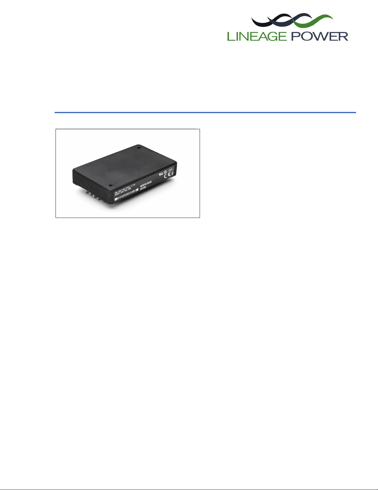
QW030xx DUAL Series Power Modules: dc-dc Converters;
18 Vdc to 36 Vdc or 36 Vdc to 75 Vdc Inputs
Features
The QW030-Series Power Modules use advanced, surfacemount technology and deliver high-quality, efficient, and
compact dc-dc conversion.
Applications
n Distributed power architectures
n Workstations
n Computer equipment
n Communications equipment
n Optical transport equipment
Options
n Heat sinks available for extended operation
n Choice of remote on/off logic configurations
n Choice of two pin lengths
n Small size: 36.8 mm x 57.9 mm x 12.7 mm
(1.45 in. x 2.28 in. x 0.50 in.)
n High power density
n High efficiency: 88% typical
n Low output noise
n Constant frequency
n Industry-standard pinout
n Metal case
n 2:1 input voltage range
n Overvoltage and overcurrent protection
n Remote on/off
n Adjustable output voltage
n ISO* 9001 and ISO 14001 Certified manufacturing
facilities
†
n UL
60950 Recognized, CSA‡ C22.2 No. 60950-00
Certified, VDE
n CE mark meets 73/23/EEC and 93/68/EEC
directives
* ISO is a registered trademark of the International Organization
for Standardization.
† UL is a registered trademark of Underwriters Laboratories, Inc.
‡ CSA is a registered trademark of Canadian Standards Assn.
§ VDE is a trademark of Verband Deutscher Elektrotechniker e.V.
**This product is intended for integration into end-use equipment.
All the required procedures for CE marking of end-use equip-
ment should be followed. (The CE mark is placed on selected
products.)
§
0805 (IEC60950) Licensed
**
Description
The QW030-Series Power Modules are dc-dc converters that operate over an input voltage range of 36 Vdc to
75 Vdc and provide precisely regulated dc outputs. The outputs are fully isolated from the inputs, allowing versatile polarity configurations and grounding connections. The modules have maximum power ratings of 30 W
to 36 W at a typical full-load efficiency of up to 88%.
These encapsulated modules offer a metal case for optimum thermal performance. Threaded-through holes are
provided to allow easy mounting or addition of a heat sink for high-temperature applications. The standard feature
set includes remote sensing, output trim, and remote on/off for convenient flexibility in distributed power
applications.
Page 2

QW030xx DUAL Series Power Modules: dc-dc Converters;
18 Vdc to 36 Vdc or 36 Vdc to 75 Vdc Inputs
Data Sheet
October 2008
Absolute Maximum Ratings
Stresses in excess of the absolute maximum ratings can cause permanent damage to the device. These are
absolute stress ratings only. Functional operation of the device is not implied at these or any other conditions in
excess of those given in the operations sections of the data sheet. Exposure to absolute maximum ratings for
extended periods can adversely affect device reliability.
Parameter Device Symbol Min Max Unit
Input Voltage:
Continuous
Transient (100 ms)
Operating Case Temperature
QW030xx
QW030xx
QW030xx Tc –40 105* °C
I
VI
VI, trans
(See Thermal Considerations section.)
Storage Temperature QW030xx T
I/O Isolation Voltage
QW030xx — — 1500 Vdc
stg –55 125 °C
(Note case is tied to input)
* Maximum case temperature varies based on power dissipation. See power derating curves for details.
—
—
—
80
100
Vdc
V
Electrical Specifications
Unless otherwise indicated, specifications apply over all operating input voltage, resistive load, and temperature
conditions.
Table 1. Input Specifications
Parameter Device Symbol Min Typ Max Unit
Operating Input Voltage:
QW030xx QW030xx V
Maximum Input Current
I = 0 V to 75 V; IO = IO, max):
(V
QW030xx QW030xx I
Inrush Transient QW030xx i
Input Reflected-ripple Current, Peak-to-peak
QW030xx I 15 — mAp-p
(5 Hz to 20 MHz, 12 µH source impedance;
see Test Configurations section.)
Input Ripple Rejection (120 Hz) QW030xx — — 50 — dB
Fusing Considerations
CAUTION: This power module is not internally fused. An input line fuse must always be used.
This encapsulated power module can be used in a wide variety of applications, ranging from simple stand-alone
operation to an integrated part of a sophisticated power architecture. To preserve maximum flexibility, internal
fusing is not included; however, to achieve maximum safety and system protection, always use an input line fuse.
The safety agencies require a normal-blow fuse with a maximum rating of 5 A (see Safety Considerations section).
Based on the information provided in this data sheet on inrush energy and maximum dc input current, the same
type of fuse with a lower rating can be used. Refer to the fuse manufacturer’s data for further information.
I 36 48 75 Vdc
I, max ——2.2 A
2
t——0.2A
2
s
2 Lineage Power
Page 3

Data Sheet
QW030xx DUAL Series Power Modules: dc-dc Converters;
October 2008
Electrical Specifications (continued)
Table 2. Output Specifications
18 Vdc to 36 Vdc or 36 Vdc to 75 Vdc Inputs
Parameter
Output Voltage Set Point
I = 48 V; IO1 = IO2,= IO,min)
(V
Output Voltage
(Over all operating input voltage, resistive
load, and temperature conditions until end of
life. See Test Configurations section.)
Device
Suffix
CL
CL
BK
BK
AJ
AJ
CL
CL
BK
BK
AJ
AJ
Symbol Min Typ Max Unit
O1, set
V
VO2, set
VO1, set
VO2, set
VO1, set
VO2, set
O1
V
VO2
VO1
VO2
VO1
VO2
14.7
-14.7
11.76
-11.76
4.85
-4.85
13.8
-13.8
11.04
-11.04
4.75
-4.75
—
—
—
—
—
—
—
—
—
—
—
—
15.3
-15.3
12.24
-12.24
5.15
-5.15
16.2
-16.2
12.96
-12.96
5.25
-5.25
Vdc
Vdc
Vdc
Vdc
Vdc
Vdc
Vdc
Vdc
Vdc
Vdc
Vdc
Vdc
Output Voltage Regulation
Line (V
Load (V
I
I = VI,min to VI,max; I01=I02)
I = VI,nom; I01 = I01min to Itot/2 and
02 = I02min to Itot/2)
Cross Regulation V
01, V02
Qx030xx
Qx030xx
Qx030xx
01,V02
V
V01+V02
V01+V02
V01,V02
V01,V02
0.5
0.25
0.25
1
±4
0.75
0.5
0.5
2
±6
%
%
%
%
(VI=VI,nom; I01 or I02= other output = max
load)
Temperature (Tc = -40 to 100)
Output Ripple and Noise Voltage
(See Test Configurations section.):
Measured across one 2.2 µF ceramic
capacitor:
RMS
Peak-to-peak (5 Hz to 20 MHz)
Qx030xx
CL
CL
BK
BK
AJ
AJ
V01,V02
—
—
—
—
—
—
—
—
—
—
—
—
0.5
1
50
150
40
120
50
150
%
mVrms
mVp-p
mVrms
mVp-p
mVrms
mVp-p
External Load Capacitance on each output Qx030xx — 0 — 220 µF
Output Current
O < IO,min the module may exceed the
(At I
ripple specifications)
Output Current-limit Inception
O = 90% of VO, set)
(V
Output Short-circuit Current (V
CL
CL
CL
BK
BK
BK
AJ
AJ
AJ
CL
BK
AJ
O = 0.25 V) CL
BK
AJ
01
I
I02
Itot
I01
I02
Itot
I01
I02
Itot
I
tot
Itot
Itot
Itotsc
Itotsc
Itotsc
0.25
0.25
!
0.5
0.25
!
0.25
0.5
0.25
!
0.25
0.5
—
—
—
—
—
—
—
—
—
—
—
—
—
—
—
3.0
3.7
7
4.5
5.5
10
1.75
1.75
2.0
2.5
2.5
3.0
3
3
6
—
—
—
—
—
—
A
A
A
A
A
A
A
A
A
A
A
A
A
A
A
* Engineering estimate.
!
Itot = I01+I02 Sum should not exceed this number
Lineage Power 3
Page 4
QW030xx DUAL Series Power Modules: dc-dc Converters;
18 Vdc to 36 Vdc or 36 Vdc to 75 Vdc Inputs
Electrical Specifications (continued)
Table 2. Output Specifications (continued)
Data Sheet
October 2008
Device
Suffix
CL
BK
AJ
Symbol Min Typ Max Unit
η
η
η
—
—
—
88
88
85
—
—
—
Efficiency (V
A = 25 °C
T
C = 25 °C
T
Parameter
I = 48 V; IO = IO, max):
Switching Frequency QW030xx — — 360 — kHz
Dynamic Response
O/Δt = 1 A/10 µs, VI = 48 V, TC = 25 °C):
(ΔI
Load Change from I
O = 50% to 75% of IO, max:
QW030xx
—
—
2.5
—
%V
Peak Deviation
Settling Time (V
Load Change from I
O < 10% of peak deviation)
O = 50% to 25% of IO, max:
QW030xx
QW030xx
—
—
—
—
5.0
2.5
—
—
%V
Peak Deviation
Settling Time (V
* Engineering estimate.
O < 10% of peak deviation)
QW030xx
—
—
5.0
—
Table 3. Isolation Specifications
Parameter Device Min Typ Max Unit
Isolation Capacitance (engineering estimate) QW030xx — 600 — pF
Isolation Resistance QW030xx 10 — — MΩ
%
%
%
O, set
ms
O, set
ms
Table 4. General Specifications
Parameter Device Min Typ Max Unit
Calculated MTBF
(I
O = 80% of IO, max; TC = 40 °C)
QW030xx 5,000,000 hours
Weight QW030xx — — 75 (2.7) g (oz.)
4 Lineage Power
Page 5

Data Sheet
October 2008
QW030xx DUAL Series Power Modules: dc-dc Converters;
18 Vdc to 36 Vdc or 36 Vdc to 75 Vdc Inputs
Feature Specifications
Unless otherwise indicated, specifications apply over all operating input voltage, resistive load, and temperature
conditions. See Feature Descriptions section of this data sheet for additional information.
Parameter
Remote On/Off Signal Interface
I = VI, min to VI, max; open collector or equivalent
(V
compatible; signal referenced to V
I(–) terminal.):
Negative Logic: Device Code Suffix “1”:
Logic Low—Module On
Logic High—Module Off
Positive Logic: If Device Code Suffix “1” Is Not
Specified:
Logic Low—Module Off
Logic High—Module On
Module Specifications:
On/Off Current—Logic Low
On/Off Voltage:
Logic Low
Logic High (I
on/off = 0 mA)
Open Collector Switch Specifications:
Leakage Current During Logic High
on/off = 15 V)
(V
Output Low Voltage During Logic Low
on/off = 1 mA)
(I
Turn-on Delay and Rise Times
(at 80% of I
O, max; TA = 25 °C):
Case 1: On/Off Input Is Set for Logic High and
then Input Power Is Applied (delay from point
at which V
I = VI, min until VO = 10% of VO, nom).
Case 2: Input Power Is Applied for at Least One
Second, and Then the On/Off Input Is Set to
Logic High (delay from point at which V
0.9 V until V
O = 10% of VO, nom).
Output Voltage Rise Time (time for V
from 10% of V
O, nom to 90% of VO, nom)
Output Voltage Overshoot (at 80% of I
A = 25 °C)
T
on/off =
O to rise
O, max;
Output Voltage Adjustment
(See Feature Descriptions section.):
Output Voltage Set-point Adjustment Range
(trim) QW030xx — 75 — 110 %V
Output Overvoltage Protection (clamp) CL
* Engineering estimate.
Device
Suffix
All
All
All
All
All
All
All
All
All
CL
BK
BK
AJ
AJ
Symbol Min Typ Max Unit
on/off
I
Von/off
Von/off
Ion/off
Von/off
delay
T
Tdelay
Trise
—
O1, ovp
V
VO2, ovp
VO1, ovp
VO2, ovp
VO1, ovp
VO2, ovp
—
–0.7
—
—
—
—
—
—
—
17.1
-17.1
13.7
-13.7
5.9
-5.9
—
—
—
—
—
8
2
10
—
—
—
—
—
—
—
1.0
1.2
15
50
1.2
—
—
—
5*
22.5
-22.5
18.0*
-18.0*
7
-7
mA
V
V
µA
V
ms
ms
ms
%
O, nom
V
V
V
V
V
V
Lineage Power 5
Page 6

QW030xx DUAL Series Power Module: dc-dc Converters; Data Sheet
18 Vdc to 36Vdc or 36 Vdc to 75 Vdc Inputs October 2008
6 Lineage Power
Page 7

Data Sheet QW030xx DUAL Series Power Module: dc-dc Converters;
October 2008 18 Vdc to 36Vdc or 36 Vdc to 75 Vdc Inputs
Lineage Power 7
Page 8

QW030xx DUAL Series Power Modules: dc-dc Converters;
18 Vdc to 36 Vdc or 36 Vdc to 75 Vdc Inputs
Data Sheet
October 2008
Design Considerations
Grounding Considerations
For the QW modules, the case is internally connected
to the V
I(+) pin.
Input Source Impedance
The power module should be connected to a low
ac-impedance input source. Highly inductive source
impedances can affect the stability of the power module. If the input source inductance exceeds 4 µH, a
33 µF electrolytic capacitor (ESR < 0.7 ohm at 100 kHz)
mounted close to the power module helps ensure stability of the unit.
Safety Considerations
QW
Modules
For safety-agency approval of the system in which the
power module is used, the power module must be
installed in compliance with the spacing and separation
requirements of the end-use safety agency standard,
i.e., UL60950, CSA C22.2 No. 60950-00, and VDE
0805 (IEC60950).
If the input source is non-SELV (ELV or a hazardous
voltage greater than 60 Vdc and less than or equal to
75 Vdc), for the module’s output to be considered
meeting the requirements of safety extra-low voltage
(SELV), all of the following must be true:
n The input source is to be provided with reinforced
insulation from any hazardous voltages, including the
ac mains.
n One VI pin and one VO pin are to be grounded, or
both the input and output pins are to be kept floating.
n The input pins of the module are not operator acces-
sible.
The power module has extra-low voltage (ELV) outputs
when all inputs are ELV.
The input to these units is to be provided with a maximum 5 A normal-blow fuse in the ungrounded lead.
Feature Descriptions
Overcurrent Protection
To provide protection in a fault (output overload) condition, the unit is equipped with internal current-limiting
circuitry and can endure current limiting for an unlimited duration. At the point of current-limit inception, the
unit shifts from voltage control to current control. If the
output voltage is pulled very low during a severe fault,
the current-limit circuit can exhibit either foldback or
tailout characteristics (output-current decrease or
increase). The unit operates normally once the output
current is brought back into its specified range.
Remote On/Off
Two remote on/off options are available. Positive logic
remote on/off turns the module on during a logic-high
voltage on the remote ON/OFF pin, and off during a
logic low. Negative logic remote on/off, device code
suffix “1,” turns the module off during logic-high voltage
and on during a logic low.
To turn the power module on and off, the user must
supply a switch to control the voltage between the
on/off terminal and the V
switch may be an open collector or equivalent (see
Figure 4). A logic low is V
maximum I
on/off during a logic low is 1 mA. The switch
should maintain a logic-low voltage while sinking 1 mA.
During a logic high, the maximum V
the power module is 15 V. The maximum allowable
leakage current of the switch at V
I(–) terminal (Von/off). The
on/off = –0.7 V to 1.2 V. The
on/off generated by
on/off = 15 V is 50 µA.
n Another SELV reliability test is conducted on the
whole system, as required by the safety agencies, on
the combination of supply source and the subject
module to verify that under a single fault, hazardous
voltages do not appear at the module’s output.
Note: Do not ground either of the input pins of the
module without grounding one of the output pins.
This may allow a non-SELV voltage to appear
between the output pin and ground.
8 Lineage Power
Page 9

Data Sheet
October 2008
QW030xx DUAL Series Power Modules: dc-dc Converters;
18 Vdc to 36 Vdc or 36 Vdc to 75 Vdc Inputs
Feature Descriptions (continued)
Remote On/Off (continued)
If not using the remote on/off feature, do one of the
following:
For positive logic, leave the ON/OFF pin open.
For negative logic, short the ON/OFF pin to V
V
I(+)
I(-)
V
-
Von/off
+
REMOTE
Ion/off
ON/OFF
Figure 4. QW030-Series Remote On/Off
Implementation
Output Voltage Set-Point Adjustment
(Trim)
I(–).
8-758(C).a
The following equation determines the required external-resistor value to obtain a change in output voltage
O, nom to VO, adj.
from V
10000 Vo,adj×
Radj-down
The voltage between the V
O2(–)and Com. terminals must not exceed the mini-
V
⎛⎞
--------------------------- --------------
⎝⎠
Vo,nom Vo,adj–
O1(+)and Com., and
- 1000=
mum output overvoltage protection value shown in the
Feature Specifications table. This limit includes any
increase in voltage due to remote-sense compensation
and output voltage set-point adjustment (trim). See Fig-
ure 5.
Consult your
Lineage Power Account Manager or
Application Engineer if the output voltage needs to be
increased more than the above limitation.
The amount of power delivered by the module is
defined as the voltage at the output terminals multiplied
by the output current. When using trim, the output voltage of the module can be increased, which at the same
output current would increase the power output of the
module. Care should be taken to ensure that the maximum output power of the module remains at or below
the maximum rated power.
Output voltage trim allows the user to increase or
decrease the output voltage set point of a module. This
is accomplished by connecting an external resistor
between the TRIM pin and either the V01(+) or V02(–)
pins. The trim resistor should be positioned close to the
module.
If not using the trim feature, leave the TRIM pin open.
With an external resistor between the TRIM and V01(+)
pins (R
adj-up), the output voltage set point (VO, adj)
increases (see Figure 5). The following equation
determines the required external-resistor value to
obtain a change in output voltage from V
Radj-up
Vo,adj
-------------------------- --------------
Vo,adj - Vo,nom
2xVo,nom
⎛⎞
• 10000 - 1000=
-------------------------
⎝⎠
1.225
O, nom to VO, adj.
-1
With an external resistor connected between the TRIM
and V02(–) pins (R
O, adj) decreases (see Figure 6).
(V
adj-down), the output voltage set point
VI(+)
ON/OFF
V
I(-)
V01
V02
(+)
NC
TRIM
COM
(-)
Radj-up
RLOAD1
RLOAD2
Figure 5. QW030-Series Circuit Configuration to
Increase Output Voltage
8-715.v
Lineage Power 9
Page 10

QW030xx DUAL Series Power Modules: dc-dc Converters;
18 Vdc to 36 Vdc or 36 Vdc to 75 Vdc Inputs
Data Sheet
October 2008
.
Feature Descriptions
(continued)
Output Voltage Set-Point Adjustment
(Trim)
Figure 6. QW030-Series Circuit Configuration to
(continued)
V
TRIM
O
V
01
(+)
COM
2(-)
R
adj-down
VI(+)
ON/OFF
V
I
(-)
Decrease Output Voltage
R
LOAD1
R
LOAD2
8-715.vf
Output Overvoltage Protection
The output overvoltage clamp consists of control
circuitry, independent of the primary regulation loop,
that monitors the voltage on the output terminals. This
control loop has a higher voltage set point than the
primary loop (see the Feature Specifications table). In
a fault condition, the overvoltage clamp ensures that
the output voltage does not exceed V
O, clamp, max
. This
provides a redundant voltage-control that reduces the
risk of output overvoltage.
Overtemperature Protection
These modules feature overtemperature protection to
safeguard the modules against thermal damage.
When the temperature exceeds the overtemperature
threshold given in the feature specifications table, the
module will limit the available output current in order to
help protect against thermal damage. The overcurrent
inception point will gradually move back to its original
level as the module is cooled below the overtemperature threshold.
Thermal Considerations
Introduction
The power modules operate in a variety of thermal
environments; however, sufficient cooling should be
provided to help ensure reliable operation of the unit.
Heat-dissipating components inside the unit are thermally coupled to the case. Heat is removed by conduction, convection, and radiation to the surrounding
environment. Proper cooling can be verified by measuring the case temperature. The case temperature
should be measured at the position indicated in
Figure 7.
33 (1.30)
14
(0.55)
Note: Top view, pin locations are for reference only.
Measurements shown in millimeters and (inches).
VI(+)
ON/OFF
VI(-)
Figure 7. QW030-Series Case Temperature
Measurement Location
The temperature at this location should not exceed
105 °C. The output power of the module should not
exceed the rated power for the module as listed in the
Ordering Information table.
Although the maximum case temperature of the power
modules is 105 °C, you can limit this temperature to a
lower value for extremely high reliability.
V
01
TRIM
COM
V
(+)
NC
02
(-)
8-2104.a
Input Undervoltage Lockout
At input voltages below the input undervoltage lockout
limit, the module operation is disabled. The module will
begin to operate at an input voltage between the undervoltage lockout limit and the minimum operating input
voltage.
10 Lineage Power
Page 11

Data Sheet
QW030xx DUAL Series Power Modules: dc-dc Converters;
October 2008
Thermal Considerations (continued)
Heat Transfer Without Heat Sinks
Increasing airflow over the module enhances the heat
transfer via convection. Figures 8 and 10 show the
maximum power that can be dissipated by the module
without exceeding the maximum case temperature versus local ambient temperature (T
tion through 3 m/s (600 ft./min.).
Systems in which these power modules may be used
typically generate natural convection airflow rates of
–1
0.3 ms
(60 ft./min.) due to other heat-dissipating components in the system. Therefore, the natural convection condition represents airflow rates of up to 0.3 ms
(60 ft./min.). Use of Figure 8 is shown in the following
example.
Example
What is the minimum airflow necessary for a
QW030BK operating at V
I = 48 V, an output current of
1.5 A, each and a maximum ambient temperature of 89
°C?
Solution
Given: V
Determine P
I = 48 V
O1 = 1.5 A, IO2 = 1.5 A
I
A = 89 °C
T
D (Use Figure 9):
P
D = 4.5 W
Determine airflow (v) (Use Figure 8):
v = 3.0 m/s (600 ft./min.)
7.0
6.0
5.0
4.0
3.0
3.0 m/s (600 ft./min.)
2.0 m/s (400 ft./min.)
2.0
1.0 m/s (200 ft./min.)
NATURAL CONVECTION
POWER DISSIPATION, PD (W)
1.0
0.0
40 50 60 70 80 90 110100
LOCAL AMBIENT TEMPERATURE, TA ( C)
A) for natural convec-
–1
MAX CASE TEMP.
1-0206
18 Vdc to 36 Vdc or 36 Vdc to 75 Vdc Inputs
6
V
I = 75 V
VI = 48 V
5
V
I = 36 V
4
3
2
1
POWER DISSIPATION, PD (W)
0
0 0.5 1 1.5 2 2.5
OUTPUT CURRENT, IO1 = IO2 (A)
Figure 9. QW030BK Power dissipation With
Balanced Loads
6
VI = 75 V
VI = 48 V
5
V
I = 36 V
4
3
2
POWER DISSIPATION, PD (W)
1
0 0.5 1 1.5 2 2.5
OUTPUT CURRENT, IO2 (A)
Figure 10. QW030BK Power Dissipation with
Unbalanced Loads with Io1 = 0.5 A
3.0
1-0204
1-0205
Figure 8. QW030BK POWER DERATING CURVE
Lineage Power 11
Page 12

QW030xx DUAL Series Power Modules: dc-dc Converters;
12
12
18 Vdc to 36 Vdc or 36 Vdc to 75 Vdc Inputs
Data Sheet
October 2008
Thermal Considerations (continued)
Heat Transfer with Heat Sinks
The power modules have through-threaded, M3 x 0.5
mounting holes, which enable heat sinks or cold plates
to attach to the module. The mounting torque must not
exceed 0.56 N-m (5 in.-lb.). For a screw attachment
from the pin side, the recommended hole size on the
customer’s PWB around the mounting holes is 0.130
± 0.005 inches. The mounting torque from the pin side
must not exceed 0.25 N-m (2.2 in.-lbs.).
Thermal derating with heat sinks is expressed by using
the overall thermal resistance of the module. Total
module thermal resistance (θca) is defined as the maximum case temperature rise (ΔT
module power dissipation (P
ΔTC max,
θca
-------------------
[]
==
PD
The location to measure case temperature (T
shown in Figure 7. Consult your Lineage Power
Account Manager or Application Engineer for case-toambient thermal resistance vs. airflow for various heat
sink configurations, heights, and orientations. Longitudinal orientation is defined as the long axis of the module that is parallel to the airflow direction, whereas in
the transverse orientation, the long axis is perpendicular to the airflow. These curves are obtained by experimental testing of heat sinks, which are offered in the
product catalog.
These measured resistances are from heat transfer
from the sides and bottom of the module as well as the
top side with the attached heat sink; therefore, the
case-to-ambient thermal resistances shown are generally lower than the resistance of the heat sink by itself.
The module used to collect the data in the case-toambient thermal resistance curves had a thermal-conductive dry pad between the case and the heat sink to
minimize contact resistance.
C, max) divided by the
D):
C TA–()
T
-----------------------P
D
C) is
Custom Heat Sinks
A more detailed model can be used to determine the
required thermal resistance of a heat sink to provide
necessary cooling. The total module resistance can be
separated into a resistance from case-to-sink (θcs) and
sink-to-ambient (θsa) as shown in Figure 11.
TC TS TA
→
PD
θcs θsa
8-1304
Figure 11. QW030-Series Resistance from Case-to-
Sink and Sink-to-Ambient
For a managed interface using thermal grease or foils,
a value of θcs = 0.1 °C/W to 0.3 °C/W is typical. The
solution for heat sink resistance is:
θsa
PD
θcs–=
TC TA–()
---------------------------
This equation assumes that all dissipated power must
be shed by the heat sink. Depending on the userdefined application environment, a more accurate
model, including heat transfer from the sides and bottom of the module, can be used. This equation provides a conservative estimate for such instances.
Layout Considerations
Copper paths must not be routed beneath the power
module standoffs. For additional layout guidelines,
refer to the FLTR100V10 or FLTR100V20 data sheet.
Lineage Power
Page 13

Data Sheet
QW030xx DUAL Series Power Modules: dc-dc Converters;
October 2008
Outline Diagram
Dimensions are in millimeters and (inches).
Tolerances: x.x mm ± 0.5 mm (x.xx in. ± 0.02 in.)
x.xx mm ± 0.25 mm (x.xxx in. ± 0.010 in.)
Top Vi e w
36.8
(1.45)
Side View
12.7
(0.50)
0.51
(0.020)
57.9
(2.28)
18 Vdc to 36 Vdc or 36 Vdc to 75 Vdc Inputs
SIDE LABEL
SIDE LABEL *
4.1 (0.16) MIN,
ALL PLACES
1.02 (0.040) DIA
SOLDER-PLATED
BRASS, ALL PLACES
6.1 (0.24), 4 PLA
Bottom View
3.6
5.3
(0.21)
(0.14)
10.9
(0.43)
15.24
(0.600)
VI(-)
ON/OFF
26.16
(1.030)
7.62
(0.300)
5.3
(0.21)
* Side label includes Lineage name, product designation, safety agency markings, input/output voltage and current ratings, and bar code.
50.80
(2.000)
47.2
(1.86)
V
COM
TRIM
V
01
3.81
(0.150)
(-)
02
11.43
(0.450)
7.62
(0.300)
Nc
(+)VI(+)
15.24
(0.600)
MOUNTING INSERTS
M3 x 0.5 THROUGH,
2 PLACES
8-1769
Lineage Power 13
Page 14

QW030xx DUAL Series Power Modules: dc-dc Converters;
18 Vdc to 36 Vdc or 36 Vdc to 75 Vdc Inputs
Recommended Hole Pattern
Component-side footprint.
Dimensions are in millimeters and (inches).
Data Sheet
October 2008
26.16
(1.030)
5.3
(0.21)
5.3
(0.21)
7.62
(0.300)
15.24
(0.600)
10.9
(0.43)
3.6
(0.14)
VI(+)
ON/OFF
I
(-)
V
47.2
(1.86)
(+)
V
01
NC
TRIM
COM
(-)
V
02
50.80
(2.000)
MOUNTING INSERTS
M3 x 0.5 THROUGH,
2 PLACES
(0.300)
3.81
(0.150)
15.24
(0.600)7.62
11.43
(0.450)
Ordering Information
Please contact your Lineage Power Account Manager or Field Application Engineer for pricing and availability.
Table 5. Device Codes
8-1769p2
Input
Volta g e
Output
Volta g e
Output
Power
Output
Current
Remote On/
Off Logic
Device
Code
48 Vdc +12, -12 36W 2.5A, 2.5A Negative QW030BK1 108958885
48 Vdc +15, -15 30W 1.75A, 1.75A Negative QW030CL1 108962176
48 Vdc +5, -5 30W 3A, 3A Negative QW030AJ1 108963687
Table 6. Device Options
Option Device Code Suffix
Short pins: 2.79 mm ± 0.25 mm
8
(0.110 in. ± 0.010 in.)
Short pins: 3.68 mm ± 0.25 mm
6
(0.145 in. ± 0.010 in.)
Negative logic On/Off 1
Comcode
14 Lineage Power
Page 15

QW030xx DUAL Series Power Modules: dc-dc Converters;OOct
18 Vdc to 36 Vdc or 36 Vdc to 75 Vdc Inputs
Advance Data Sheet
April 2008
Asia-Pacific Headquarter s
Tel: +65 6 416 4283
World Wide Headquarters
Lineag e Po w er Co rp or a tio n
30 00 Skyline Drive, Mesquite, TX 75149, U SA
+1-800-526-7819
(Outsid e U.S.A.: +1-972-2 84-2626)
ww w.line ag ep ower .co m
e-m ail: techsupport1@lineagepower.com
Lineage Power reserves the right to m ake changes to the produc t(s) or information contained herein without notice. No liability is assumed as a result of their use or
application. No rights under any patent accompany the sale of any suc h pr oduct(s) or information.
© 2008 Lineage Power Corporation, (Mesquite, Texas) All International Rights Reser ved.
Europe, Middle-East and Africa Head quarters
Tel: +49 8 9 6089 286
India Headquarters
Tel: +91 8 0 28411633
October 2008
ADS01-046EPS (Replaces
ADS01-045EPS)
 Loading...