

Page 1
Data Sheet
f
August 24, 2010
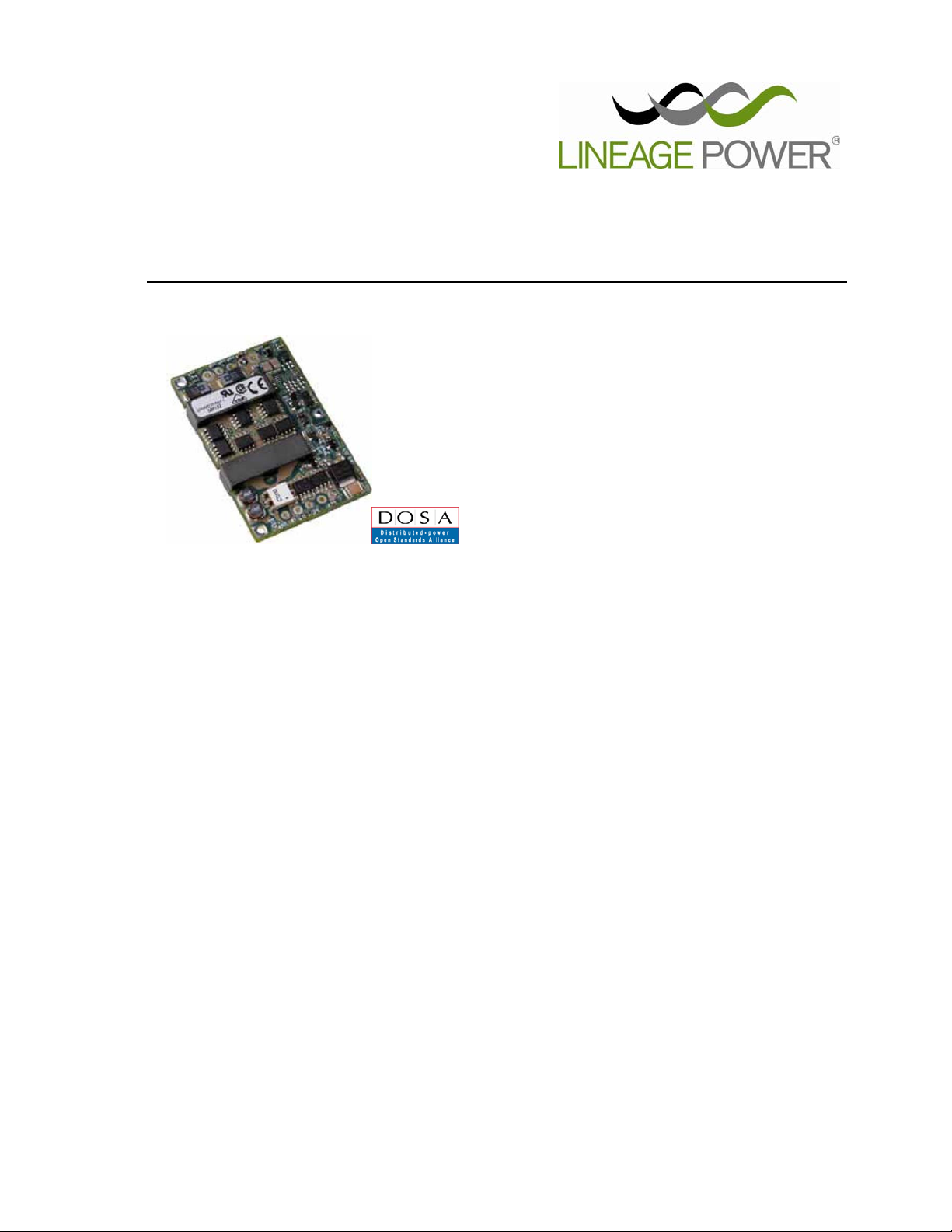
QRW010/025/035/040 Series Power Modules; dc-dc Converters
36 Vdc - 75 Vdc Input, 1.0 to 12 Vdc Output; 10 A to 40 A
RoHS Compliant
Applications
Enterprise Networks
Wireless Networks
Access and Optical Network Equipment
Enterprise Networks
Latest generation IC’s (DSP, FPGA, ASIC) and
Microprocessor-powered applications.
Options
Positive Remote On/Off logic
Case ground pin (-H Base plate version)
Auto restart after fault shutdown
Description
The QRW-series dc-dc converters are a new generation of DC/DC power modules designed for optimum efficiency
and power density. The QRW series provide up to 40A output current in an industry standard quarter brick, which
makes it an ideal choice for small space, high current and low voltage applications. The converter uses synchronous
rectification technology and innovative packaging techniques to achieve ultra high e fficiency reaching 91% at 3.3V
full load. Thanks to the ultra high efficiency of this converter, the power dissipation is such t hat for most applications
a heat sink is not required. In addition, the QRW-series supports future migration of semiconductor and
microprocessor supply voltages do wn to 1.0V .
Features
Compliant to RoHS EU Directive 2002/95/EC (-Z
versions)
Compliant to ROHS EU Directive 2002/95/EC with
lead solder exemption (non-Z ve rsions)
Delivers up to 40A output current
Ultra High efficiency – 91% at 3.3V full load
Industry standard DOSA Compliant Quarter brick:
57.9 mm x 36.8 mm x 9.5 mm
(2.28 in x 1.45 in x 0.375 in)
Improved Thermal Performance:
23A at 70ºC at 1m/s (200LFM) for 3.3Vo
High power density: 100W/in
3
Low output ripple and noise
Low output voltages down to 1V: Supports migration
to future IC and microprocessor supply voltages
2:1 input voltage
Remote Sense
Remote On/Off
Constant switching frequency
Output overvoltage and Overcurrent protection
Overtemperature protection
Adjustable output voltage (+10% / -20%)
Meets the voltage isolation requirements for
ETSI 300-132-2 and complies with and is licensed
for Basic Insulation rating per EN60950-1
UL** 60950-1 Recognised, CSA
1-03 Certified, and VDE
‡
†
C22.2 No. 60950-
0805 (IEC60950, 3rd
Edition) Licensed
CE mark meets 2006/95/EC directive
ISO* 9001 certified manufacturing facilities
§
* ISO is a registered trademark of the International Organization of Standards
** UL is a registered trademark of Underwriters Laboratories, Inc.
†
CSA is a registered trademark of Canadian Standards Association.
‡
VDE is a trademark of Verband Deutscher Elektrotechniker e.V.
§ This product is intended for integration into end-use equipment. All of the required procedures of end-use equipment
should be followed.
Document Name: DS03-113 ver.4.4
PDF name:
QRW035_Series.pd
Page 2
Data Sheet
August 24, 2010
QRW010/025/035/040 Series Power Modules; dc-dc Converters
36 Vdc - 75 Vdc Input, 1.0 to 12 Vdc Output; 10 A to 40 A
Absolute Maximum Ratings
Stresses in excess of the absolute maximum ratings can cause permanent damage to the device. These are absolute stress
ratings only, functional operation of the device is not implied at these or any other conditions in excess of those given in the
operations sections of the data sheet. Exposure to absolute maximum ratings for extended periods can adversely affect the
device reliabiltiy.
Parameter Device Symbol Min Max Unit
Input Voltage:Continuous
Transient (100ms)
Operating Ambient Temperature
(See Thermal Considerations section)
Storage Temperature All Tstg –55 125 °C
I/O Isolation Voltage (100% factory Hi-Pot tested)
When using optional case ground pin
(option 7)
All VI
VI, trans
All TA –40 85 °C
— — 1500
—
—
700
80
100
Vdc
Vdc
Vdc
Vdc
Electrical Specifications
Unless otherwise indicated, specifications apply over all operating input voltage, resistive load, and temperature conditions.
Parameter Device Symbol Min Typ Max Unit
Operating Input Voltage All VIN 36 48 75 Vdc
Maximum Input Current
(VI = 0 V to 75 V; IO = IO, max)
Inrush Transient All I
Input Reflected Ripple Current, peak-peak
(5 Hz to 20 MHz, 12 µH source impedance
See Test configuration section)
Input Ripple Rejection (120 Hz) All 60 dB
All — — 4.5 Adc
2
t1A
All 16 mAp-p
2
s
CAUTION: This power module is not internally fused. An input line fuse must always be used.
This power module can be used in a wide variety of applications, ranging from simple stand-alone operation to an integrated
part of a sophisticated power architecture. To preserve maximum flexibility, internal fusing is not included; however, to achieve
maximum safety and system protection, always use an input line fuse. The safety agencies require a normal-blow fuse with a
maximum rating of 10 A (see Safety Considerations section). Based on the information provided in this data sheet on inrush
energy and maximum dc input current, the same type of fuse with a lower rating can be used. Refer to the fuse manufacturer’s
data for further information.
Lineage Power 2
Page 3
Data Sheet
August 24, 2010
QRW010/025/035/040 Series Power Modules; dc-dc Converters
36 Vdc - 75 Vdc Input, 1.0 to 12 Vdc Output; 10 A to 40 A
Electrical Specifications (continued)
Output Specifications for the QRW040A0S1R0 (Vo = 1.0Vdc)
Parameter Device Symbol Min Typ Max Unit
Output Voltage Set Point
(VI = 48 Vdc; IO = IO, min to IO, max, TA = 25 °C)
Output Voltage
(Over all operating input voltage, resistive load, and
temperature conditions at steady state until end of life.)
Output Regulation:
Line (VI = VI, min to VI, max)
Load (IO = IO, min to IO, max)
Temperature (TA = TA, min to TA, max)
Output Ripple and Noise
RMS (5 Hz to 20 MHz bandwidth)
Peak-to-peak (5 Hz to 20 MHz bandwidth)
External Load Capacitance — 25,000 µF
Output Current
(Vo =90% of VO, nom.)
Output Current-limit Inception
(VO = 90% of VO, set)
Output Short-circuit Current (Average)VO = 0.25 V Latched off
Efficiency
(VI = VIN, nom; IO = IO, max), TA = 25 °C
Switching Frequency All fSW — 300 — kHz
Dynamic Response
(DIO/Dt = 1 A/10 µs, VI = 48 V, TA = 25 °C); tested
with a 220 µF aluminium and a 1.0 µf ceramic
capacitor across the load.):
Load Change from
IO = 50% to 75% of IO, max:
Peak Deviation
Settling Time
(VO < 10% of peak deviation)
Load Change from IO = 50% to 25%
of IO, max :
Peak Deviation
Settling Time
(VO < 10% of peak deviation)
P Vo 0.99 1.0 1.01 Vdc
P Vo 0.98 — 1.02 Vdc
P—
—
—
P—
PIO0.0—40Adc
P IO, lim — 49 — Adc
η —83— %
—
—
—
—
0.1
0.1
15
—
—
160
200
180
200
0.3
0.3
50
30
80
%, VO, set
%, VO, set
mVrms
mVp-p
mV
mV
µs
mV
µs
Isolation Specifications
Parameter Symbol Min Typ Max Unit
Isolation Capacitance Ciso — 5600 — PF
Isolation Resistance Riso 10 — — MΩ
General Specifications
Parameter Min Typ Max Unit
Calculated MTBF (Io = 80% of Io, max Ta = 40 °C TBD
Weight — 37(1.31) — g (oz.)
Lineage Power 3
Hours
Page 4
Data Sheet
August 24, 2010
QRW010/025/035/040 Series Power Modules; dc-dc Converters
36 Vdc - 75 Vdc Input, 1.0 to 12 Vdc Output; 10 A to 40 A
Feature Specifications
Unless otherwise indicated, specifications apply over all operating input voltage, resistive load, and temperature conditions.
See Feature Descriptions for additional information
Parameter Symbol Min Typ Max Unit
Remote On/Off Signal Interface*
(VI = 0 V to 75 V; open collector or equivalent compatible; signal
referenced to VI(–) terminal; see Figure 52
and Feature Descriptions.):
Preferred Logic:
Logic Low—Module On
Logic High—Module Off
Optional Logic:
Logic Low—Module Off
Logic High—Module On
Logic Low:
At Ion/off = 1.0 mA
At Von/off = 0.0 V
Logic High:
At Ion/off = 0.0 µA
Leakage Current
Turn-on Time; see Typical Start-up Curve(IO = IO max;
Vo within ±1% of steady state)
Output Voltage Adjustment
(See Feature Descriptions):
Output Voltage Remote-sense Range
Output Voltage Set-point Adjustment Range (trim)
.
Von/off
Ion/off
Von/off
Ion/off
—
—
—
—
—
—
80
0
—
—
—
—
2
—
—
1.2
1.0
15
50
4
10
110
V
mA
V
µA
ms
%VO,rated
%V0,nom
Output Overvoltage Protection VO, ovsd 1.25 — 1.5 V
Overtemperature Protection (IO = IO, max) T
ref1 — 127 — °C
Lineage Power 4
Page 5
Data Sheet
August 24, 2010
QRW010/025/035/040 Series Power Modules; dc-dc Converters
36 Vdc - 75 Vdc Input, 1.0 to 12 Vdc Output; 10 A to 40 A
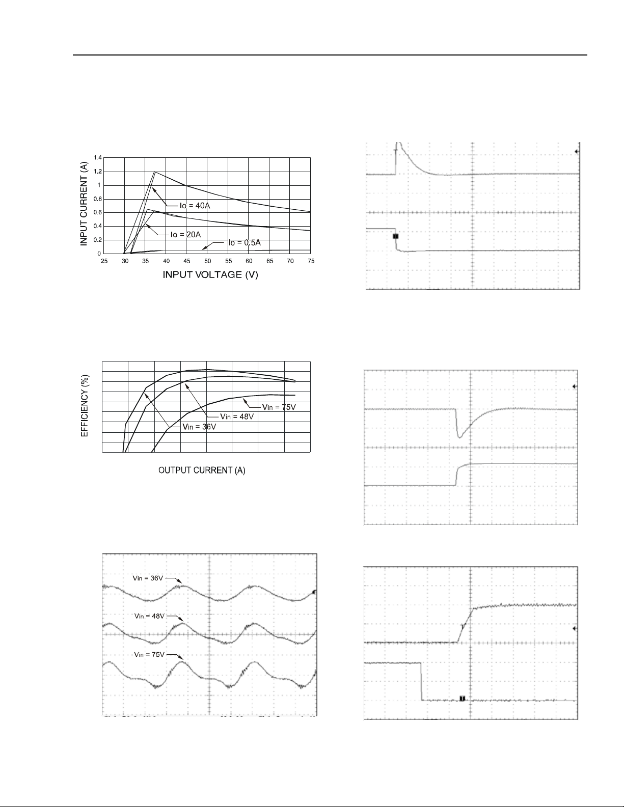
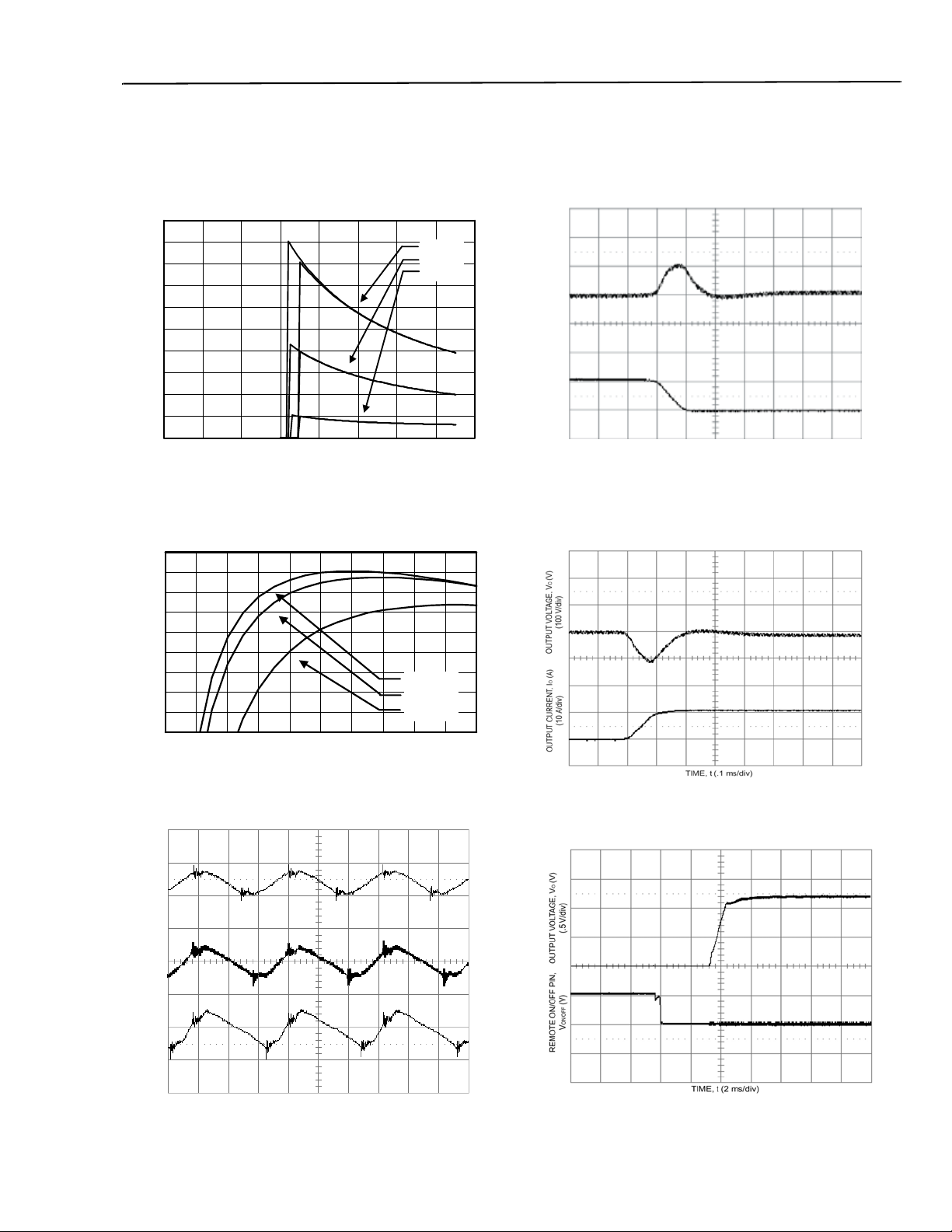
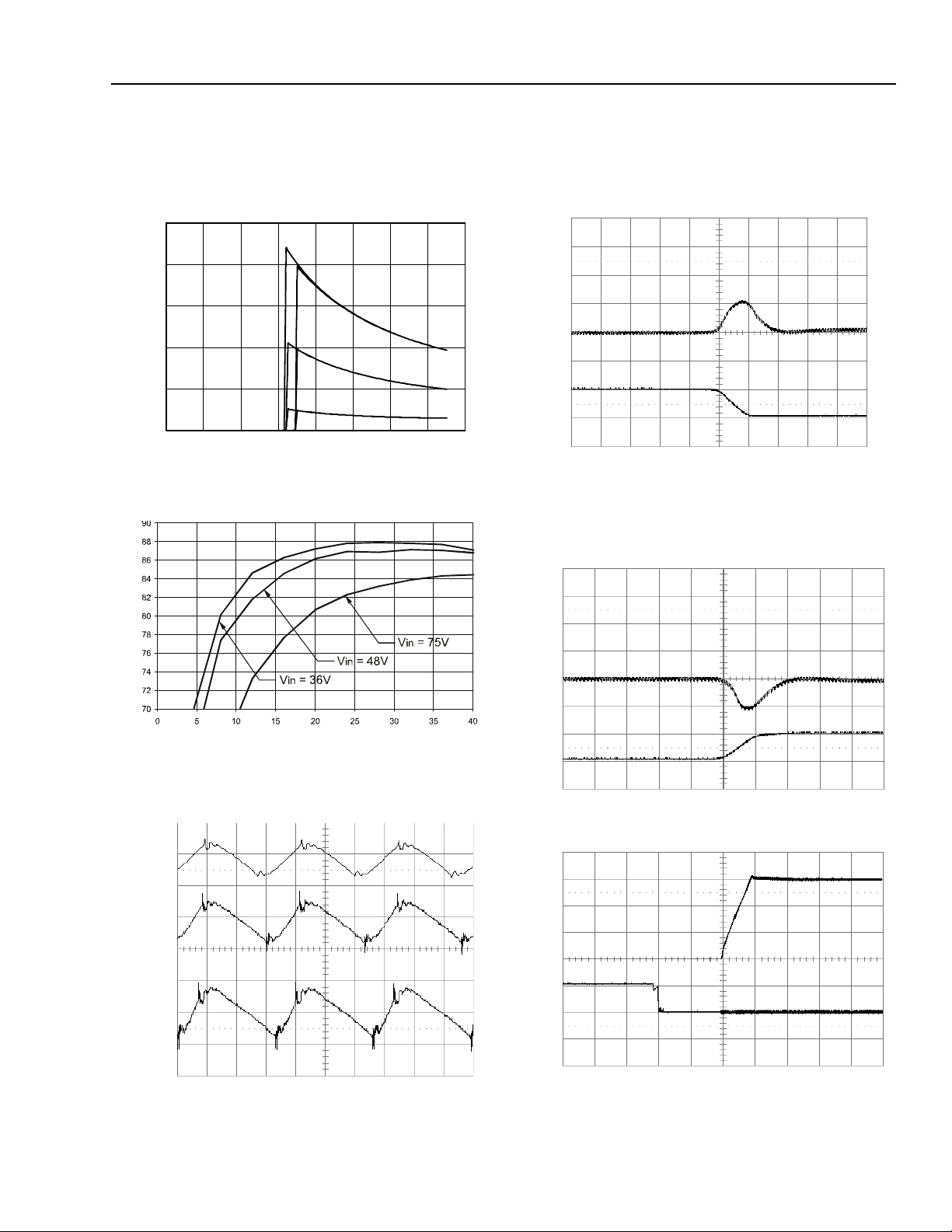
Characteristic Curves
The following figures provide typical characteristics curves for the QRW040A0S1R0 (VO = 1.0 V) module at room temperature
(TA = 25 °C).The figures are identical for both on/off configurations.
Vo ( V
(100 mv/div)
OUTPUT CURRENT,
(10A/div)
OUTPUT VOLTAGE, Io (A)
TIME, t (0.1ms/div)
Tested with a 220µF aluminium and a 1.0µF ceramic
Figure 1. Input Voltage and Current Characteristics.
88
86
84
82
80
78
76
74
72
70
0 5 10 15 20 25 30 35 40
capacitor across the load.
Figure 4. Transient Response to Step decrease in
Load from 50% to 25% of Full Load (VI = 48
Vdc).
Vo ( V)
(100 mv/div)
OUTPUT CURRENT,
(10A/div)
OUTPUT VOLTAGE, Io (A)
Figure 2. Converter Efficiency vs. Output Current.
TIME, t (0.1ms/div)
Figure 5. Transient Response to Step Increase in Load
from 50% to 75% of Full Load (VI = 48 Vdc).
(V)
(0.5 V/div)
OUTPUT VOLTAGE
(50 mV/div)
OUTPUT VOLTAGE, Vo (V)
V on/off (V)
REMOTE ON/OFF
TIME, t (1.00 µs/div)
Figure 3. Output Ripple Voltage (IO = IO, max).
Figure 6. Start-up from Remote On/Off (IO = IO, max).
TIME, t (2ms/div)
Lineage Power 5
Page 6

Data Sheet
August 24, 2010
QRW010/025/035/040 Series Power Modules; dc-dc Converters
36 Vdc - 75 Vdc Input, 1.0 to 12 Vdc Output; 10 A to 40 A
Electrical Specifications (continued)
Output Specifications for the QRW040AP (Vo = 1.2Vdc)
Parameter Device Symbol Min Typ Max Unit
Output Voltage Set Point
(VI = 48 Vdc; IO = IO, min to IO, max, TA = 25 °C)
Output Voltage
(Over all operating input voltage, resistive load, and
temperature conditions at steady state until end of life.)
Output Regulation:
Line (VI = VI, min to VI, max)
Load (IO = IO, min to IO, max)
Temperature (TA = TA, min to TA, max)
Output Ripple and Noise
RMS (5 Hz to 20 MHz bandwidth)
Peak-to-peak (5 Hz to 20 MHz bandwidth)
External Load Capacitance — 25,000 µF
Output Current
(Vo =90% of VO, nom.)
Output Current-limit Inception
(VO = 90% of VO, set)
Output Short-circuit Current (Average)VO = 0.25 V Latched off
Efficiency
(VI = VIN, nom; IO = IO, max), TA = 25 °C
Switching Frequency All fSW — 300 — kHz
Dynamic Response
(DIO/Dt = 1 A/10 µs, VI = 48 V, TA = 25 °C); tested
with a 220 µF aluminium and a 1.0 µf ceramic
capacitor across the load.):
Load Change from
IO = 50% to 75% of IO, max:
Peak Deviation
Settling Time
(VO < 10% of peak deviation)
Load Change from IO = 50% to 25%
of IO, max :
Peak Deviation
Settling Time
(VO < 10% of peak deviation)
P Vo 1.18 1.2 1.22 Vdc
P Vo 1.16 — 1.24 Vdc
P—
—
—
P—
PIO0.0—40Adc
P IO, lim — 45 — Adc
η —85— %
—
—
—
—
0.05
0.05
15
—
—
120
200
120
200
0.3
0.3
50
30
80
%, VO, set
%, VO, set
mVrms
mVp-p
mV
mV
µs
mV
µs
Isolation Specifications
Parameter Symbol Min Typ Max Unit
Isolation Capacitance Ciso — 5600 — PF
Isolation Resistance Riso 10 — — MΩ
General Specifications
Parameter Min Typ Max Unit
Calculated MTBF (Io = 80% of Io, max Ta = 40 °C), Issue 1, M1, C1 1,271,000 Hour
Weight — 37(1.31) — g
Lineage Power 6
s
(oz.)
Page 7

Data Sheet
August 24, 2010
QRW010/025/035/040 Series Power Modules; dc-dc Converters
36 Vdc - 75 Vdc Input, 1.0 to 12 Vdc Output; 10 A to 40 A
Feature Specifications
Unless otherwise indicated, specifications apply over all operating input voltage, resistive load, and temperature conditions.
See Feature Descriptions for additional information
Parameter Symbol Min Typ Max Unit
Remote On/Off Signal Interface*
(VI = 0 V to 75 V; open collector or equivalent compatible; signal
referenced to VI(–) terminal; see Figure 52
and Feature Descriptions.):
Preferred Logic:
Logic Low—Module On
Logic High—Module Off
Optional Logic:
Logic Low—Module Off
Logic High—Module On
Logic Low:
At Ion/off = 1.0 mA
At Von/off = 0.0 V
Logic High:
At Ion/off = 0.0 µA
Leakage Current
Turn-on Time; see Typical Start-up Curve(IO = IO max;
Vo within ±1% of steady state)
Output Voltage Adjustment
(See Feature Descriptions):
Output Voltage Remote-sense Range
Output Voltage Set-point Adjustment Range (trim)
Output Overvoltage Protection VO, ovsd 1.42 — 1.58 V
Overtemperature Protection (IO = IO, max) T
* A Minimum OFF Period of 1 sec is recommended.
.
Von/off
Ion/off
Von/off
Ion/off
—
—
ref1 — 127 — °C
—
—
—
—
80
0
—
—
—
—
2
—
—
1.2
1.0
15
50
4
10
110
V
mA
V
µA
ms
%VO,rated
%V0,nom
Lineage Power 7
Page 8
Data Sheet
88
August 24, 2010
QRW010/025/035/040 Series Power Modules; dc-dc Converters
36 Vdc - 75 Vdc Input, 1.0 to 12 Vdc Output; 10 A to 40 A
Characteristic Curves
The following figures provide typical characteristics curves for the QRW040A0P (VO = 1.2 V) module at room temperature (TA
= 25 °C)
2
1.8
1.6
1.4
(A)
I
1.2
1
0.8
0.6
INPUT CURRENT, I
0.4
0.2
0
0 102030405060 7080
IO = 40 A
I
= 20 A
O
I
= 4 A
O
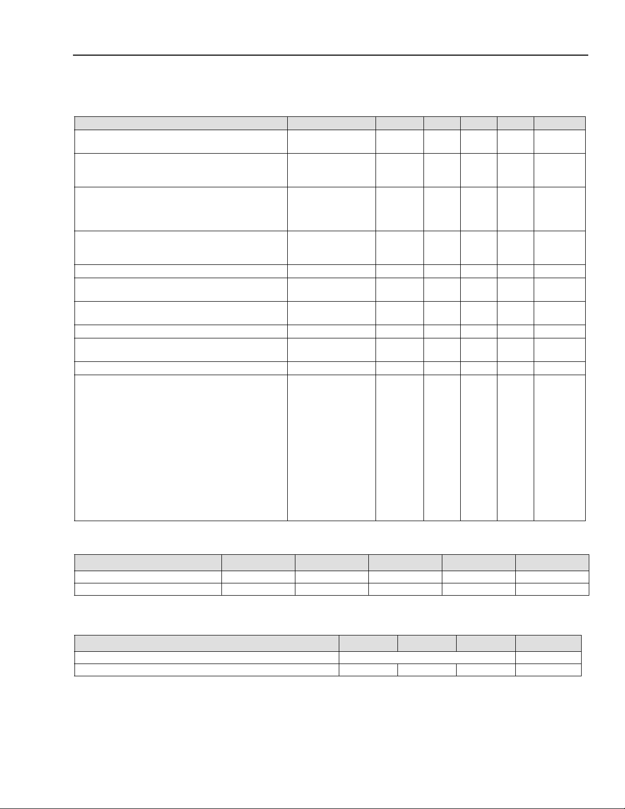
Figure 7. Input Voltage and Current Characteristics.
86
84
82
(%)
η
80
78
76
EFFICIENCY,
74
72
70
0 4 8 1216202428323640
OUTPUT CURRENT, I
VI = 36 V
= 48 V
V
I
= 75 V
V
I
(A)
O
Figure 8. Converter Efficiency vs. Output Current.
O
(100 mV/div)
OUTPUT VOLTAGE, V (V)
O
(10 A/div)
OUTPUT CURRENT, I (A)
TIME, t (.1 ms/div)
Tested with a 220µF aluminium and a 1.0µF ceramic
capacitor across the load.
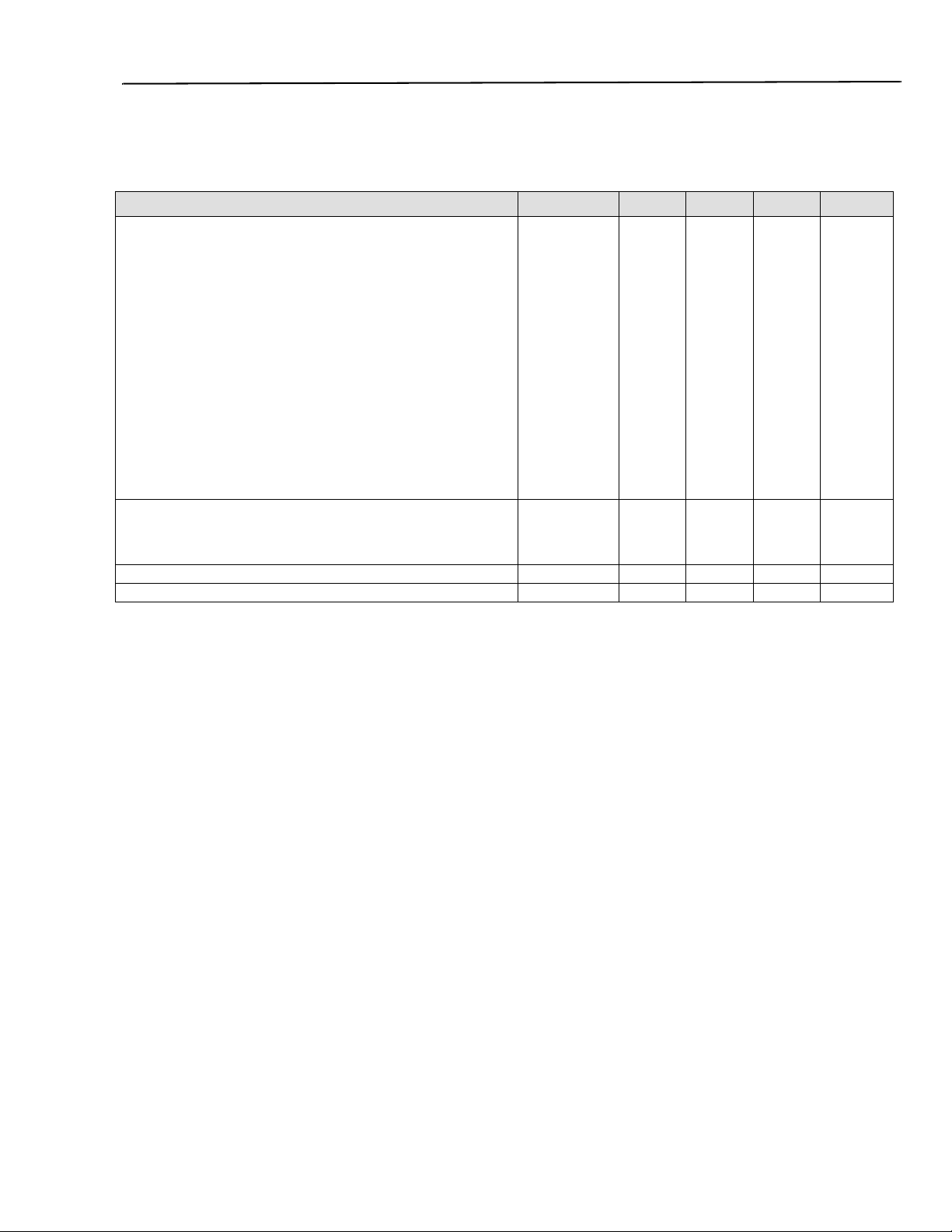
Figure 10. Transient Response to Step Decrease in
Load from 50% to 25% of Full Load
(VI = 48 Vdc).
Figure 11. Transient Response to Step Increase in
Load from 50% to 75% of Full Load
(VI = 48 Vdc).
36V, 40A
48V, 40A
(50 mV/div)
OUTPUT VOL TA GE, VO (V)
75V, 40A
TIME t, (1µs/div)
Figure 9. Output Ripple Voltage (IO = IO, max).
Tested with a 10µF aluminium and a 1.0µF tantalum capacitor
across the load.
Figure 12. Start-up from Remote On/Off (IO = IO, max).
Lineage Power 8
Page 9
Data Sheet
August 24, 2010
QRW010/025/035/040 Series Power Modules; dc-dc Converters
36 Vdc - 75 Vdc Input, 1.0 to 12 Vdc Output; 10 A to 40 A
Electrical Specifications (continued)
Output Specifications for the QRW040AOM (Vo = 1.5Vdc)
Parameter Device Symbol Min Typ Max Unit
Output Voltage Set Point
(VI = 48 Vdc; IO = IO, min to IO, max, TA = 25 °C)
Output Voltage
(Over all operating input voltage, resistive load, and
temperature conditions at steady state until end of life.)
Output Regulation:
Line (VI = VI, min to VI, max)
Load (IO = IO, min to IO, max)
Temperature (TA = TA, min to TA, max)
Output Ripple and Noise
RMS (5 Hz to 20 MHz bandwidth)
Peak-to-peak (5 Hz to 20 MHz bandwidth)
External Load Capacitance — 25,000 µF
Output Current
(Vo =90% of VO, nom.)
Output Current-limit Inception
(VO = 90% of VO, set)
Output Short-circuit Current (Average)VO = 0.25 V Latched off
Efficiency
(VI = VIN, nom; IO = IO, max), TA = 25 °C
Switching Frequency All fSW — 300 — kHz
Dynamic Response
(DIO/Dt = 1 A/10 µs, VI = 48 V, TA = 25 °C); tested
with a 220 µF aluminium and a 1.0 µf ceramic
capacitor across the load.):
Load Change from
IO = 50% to 75% of IO, max:
Peak Deviation
Settling Time
(VO < 10% of peak deviation)
Load Change from IO = 50% to 25%
of IO, max :
Peak Deviation
Settling Time
(VO < 10% of peak deviation)
MVo1.471.51.52Vdc
MVo1.45—1.55Vdc
M—
—
—
M—
MIO0.0—40Adc
M IO, lim — 47 — Adc
η —86.5— %
—
—
—
—
0.05
0.05
15
—
—
120
200
120
200
0.2
0.2
50
20
100
%, VO, set
%, VO, set
mVrms
mVp-p
mV
mV
µs
mV
µs
Isolation Specifications
Parameter Symbol Min Typ Max Unit
Isolation Capacitance Ciso — 5600 — PF
Isolation Resistance Riso 10 — — MΩ
General Specifications
Parameter Min Typ Max Unit
Calculated MTBF (Io = 80% of Io, max Ta = 40 °C)
Weight — 38(1.54)
Lineage Power 9
, Issue 1, M1, C1 1,548,000 Hours
— g (oz.)
Page 10
Data Sheet
August 24, 2010
QRW010/025/035/040 Series Power Modules; dc-dc Converters
36 Vdc - 75 Vdc Input, 1.0 to 12 Vdc Output; 10 A to 40 A
Feature Specifications
Unless otherwise indicated, specifications apply over all operating input voltage, resistive load, and temperature conditions.
See Feature Descriptions for additional information
Parameter Symbol Min Typ Max Unit
Remote On/Off Signal Interface*
(VI = 0 V to 75 V; open collector or equivalent compatible; signal
referenced to VI(–) terminal; see Figure 52
and Feature Descriptions.):
Preferred Logic:
Logic Low—Module On
Logic High—Module Off
Optional Logic:
Logic Low—Module Off
Logic High—Module On
Logic Low:
At Ion/off = 1.0 mA
At Von/off = 0.0 V
Logic High:
At Ion/off = 0.0 µA
Leakage Current
Turn-on Time; see Typical Start-up Curve(IO = IO max;
Vo within ±1% of steady state)
Output Voltage Adjustment
(See Feature Descriptions):
Output Voltage Remote-sense Range
Output Voltage Set-point Adjustment Range (trim)
Output Overvoltage Protection VO, ovsd 1.69 — 2.07 V
Overtemperature Protection (IO = IO, max) T
* A Minimum OFF Period of 1 sec is recommended.
.
Von/off
Ion/off
Von/off
Ion/off
—
—
ref1 — 127 — °C
—
—
—
—
80
0
—
—
—
—
2
—
—
1.2
1.0
15
50
4
10
110
V
mA
V
µA
ms
%VO,rated
%V0,nom
Lineage Power 10
Page 11
Data Sheet
June 2, 2009
QRW010/025/035/040 Series Power Modules; dc-dc Converters
36 Vdc - 75 Vdc Input, 1.0 to 12 Vdc Output; 10 A to 40 A
Characteristic Curves
The following figures provide typical characteristics curves for the QRW040A0M (VO = 1.5 V) module at room temperature (TA
= 25 °C)
2.5
2
(A)
I
1.5
1
INPUT CURRENT, I
0.5
0
0 1020304050607080
INPUT VOLTAGE, V
(V)
I
Figure 13. Input Voltage and Current Characteristics.
η
EFFICIENCY, ( %)
(V)
O
(100 mV/div)
OUTPUT VOL TA GE, V
(A)
O
(10 A/div)
OUTPUT CURRENT, I
TIME, t (.1 ms/div)
Tested with a 220µF aluminium and a 1.0µF ceramic capacitor
across the load.
Figure 16. Transient Response to Step Decrease in
Load from 50% to 25% of Full Load (VI = 48
Vdc).
(V)
O
(100 mV/div)
OUTPUT VOL TA GE, V
OUTPUT CURRENT, Io (A)
Figure 14. Converter Efficiency vs. Output Current.
36V, 40A
(V)
O
V
(50 mV/div)
OUTPUT VOL TA GE,
Figure 15. Output Ripple Voltage (IO = IO, max).
48V, 40A
75V, 40A
TIME,t (1 µs/div)
(A)
O
(10 A/div)
OUTPUT CURRENT, I
TIME, t (.1 ms/div)
Figure 17. Transient Response to Step Increase in Load
from 50% to 75% of Full Load (VI = 48 Vdc).
(V)
O
(.5 V/div)
OUTPUT VOL TA GE, V
(V)
ON/OFF
V
REMOTE ON/OFF PIN,
TIME, t (2 ms/div)
Tested with a 10µF aluminium and a 1.0µF tantalum capacitor across
the load.
Figure 18. Start-up from Remote On/Off (IO = IO, max).
Lineage Power 11
Page 12
Data Sheet
August 24, 2010
QRW010/025/035/040 Series Power Modules; dc-dc Converters
36 Vdc - 75 Vdc Input, 1.0 to 12 Vdc Output; 10 A to 40 A
Electrical Specifications (continued)
Output Specifications for the QRW040A0Y (Vo = 1.8Vdc)
Parameter Device Symbol Min Typ Max Unit
Output Voltage Set Point
(VI = 48 Vdc; IO = IO, min to IO, max, TA = 25 °C)
Output Voltage
(Over all operating input voltage, resistive load, and
temperature conditions at steady state until end of life.)
Output Regulation:
Line (VI = VI, min to VI, max)
Load (IO = IO, min to IO, max)
Temperature (TA = TA, min to TA, max)
Output Ripple and Noise
RMS (5 Hz to 20 MHz bandwidth)
Peak-to-peak (5 Hz to 20 MHz bandwidth)
External Load Capacitance — 25,000 µF
Output Current
(Vo =90% of VO, nom.)
Output Current-limit Inception
(VO = 90% of VO, set)
Output Short-circuit Current (Average)VO = 0.25 V Latched off
Efficiency
(VI = VIN, nom; IO = IO, max), TA = 25 °C
Switching Frequency All fSW — 300 — kHz
Dynamic Response
(DIO/Dt = 1 A/10 µs, VI = 48 V, TA = 25 °C); tested
with a 220 µF aluminium and a 1.0 µf ceramic
capacitor across the load.):
Load Change from
IO = 50% to 75% of IO, max:
Peak Deviation
Settling Time
(VO < 10% of peak deviation)
Load Change from IO = 50% to 25%
of IO, max :
Peak Deviation
Settling Time
(VO < 10% of peak deviation)
Y Vo 1.77 1.8 1.83 Vdc
Y Vo 1.75 — 1.85 Vdc
Y—
—
—
Y—
YIO0.0—40Adc
Y IO, lim — 45 — Adc
η —88— %
—
—
—
—
0.05
0.05
15
—
—
200
200
200
200
0.2
0.2
50
35
100
%, VO, set
%, VO, set
mVrms
mVp-p
mV
mV
µs
mV
µs
Isolation Specifications
Parameter Symbol Min Typ Max Unit
Isolation Capacitance Ciso — 5600 — PF
Isolation Resistance Riso 10 — — MΩ
General Specifications
Parameter Min Typ Max Unit
Calculated MTBF (IO = 80% of IO, max TA = 40 °C) TBD Hours
Weight — 38(1.34) — g (oz.)
Lineage Power 12
Page 13

Data Sheet
August 24, 2010
QRW010/025/035/040 Series Power Modules; dc-dc Converters
36 Vdc - 75 Vdc Input, 1.0 to 12 Vdc Output; 10 A to 40 A
Feature Specifications
Unless otherwise indicated, specifications apply over all operating input voltage, resistive load, and temperature conditions.
See Feature Descriptions for additional information
Parameter Symbol Min Typ Max Unit
Remote On/Off Signal Interface*
(VI = 0 V to 75 V; open collector or equivalent compatible; signal
referenced to VI(–) terminal; see Figure 52
and Feature Descriptions.):
Preferred Logic:
Logic Low—Module On
Logic High—Module Off
Optional Logic:
Logic Low—Module Off
Logic High—Module On
Logic Low:
At Ion/off = 1.0 mA
At Von/off = 0.0 V
Logic High:
At Ion/off = 0.0 µA
Leakage Current
Turn-on Time; see Typical Start-up Curve(IO = IO max;
Vo within ±1% of steady state)
Output Voltage Adjustment
(See Feature Descriptions):
Output Voltage Remote-sense Range
Output Voltage Set-point Adjustment Range (trim)
Output Overvoltage Protection VO, ovsd 2.0 — 2.5 V
Overtemperature Protection (IO = IO, max) T
* A Minimum OFF Period of 1 sec is recommended.
.
Von/off
Ion/off
Von/off
Ion/off
—
—
ref1 — 127 — °C
—
—
—
—
80
0
—
—
—
—
2
—
—
1.2
1.0
15
50
4
10
110
V
mA
V
µA
ms
%VO,rated
%V0,nom
Lineage Power 13
Page 14

Data Sheet
3.0
0
August 24, 2010
QRW010/025/035/040 Series Power Modules; dc-dc Converters
36 Vdc - 75 Vdc Input, 1.0 to 12 Vdc Output; 10 A to 40 A
Characteristic Curves
The following figures provide typical characteristics curves for the QRW040A0Y (VO = 1.8 V) module at room temperature (TA
= 25 °C)
2.5
2.0
1.5
1.0
INPUT CURRENT, II (A)
0.5
0
0 2040608
INPUT VOLTAGE, VI (V)
Figure 19. Input Voltage and Current Characteristics.
IO = 100%
IO = 50%
IO = 10%
(V) (100 mV/div)
O
V
OUTPUT VOLTA GE,
(A) (10 A/div)
O
I
OUTPUT CURRENT,
TIME, t (0.1 ms/div)
Tested with a 220µF aluminium and a 1.0µF ceramic capacitor
across the load.
Figure 22. Transient Response to Step Decrease in
Load from 50% to 25% of Full Load
(VI = 48 Vdc).
η
EFFICIENCY, ( %)
OUTPUT CURRENT, Io (A)
Figure 20. Converter Efficiency vs. Output Current.
VI = 36 V
(V)
O
VI = 48 V
(50 mV/div)
OUTPUT VOLT AGE, V
Figure 21. Output Ripple Voltage (IO = IO, max).
VI = 75 V
TIME, t (1 µs/div)
(V) (100 mV/div)
O
V
OUTPUT VOLTA GE,
(A) (10 A/div)
O
I
OUTPUT CURRENT,
TIME, t (0.1 ms/div)
Figure 23. Transient Response to Step Increase in
Load from 50% to 75% of Full Load
(VI = 48 Vdc).
(V) (0.5 V/div)
O
V
OUTPUT VOLTA GE,
(5 V/div)
ON/OFF
V
REMOTE ON/OFF,
TIME, t (2 ms/div)
Tested with a 10µF aluminium and a 1.0µF tantalum capacitor
across the load.
Figure 24. Start-up from Remote On/Off (IO = IO, max).
Lineage Power 14
Page 15

Data Sheet
August 24, 2010
QRW010/025/035/040 Series Power Modules; dc-dc Converters
36 Vdc - 75 Vdc Input, 1.0 to 12 Vdc Output; 10 A to 40 A
Electrical Specifications (continued)
Output Specifications for the QRW035A0G (Vo = 2.5Vdc)
Parameter Device Symbol Min Typ Max Unit
Output Voltage Set Point
(VI = 48 Vdc; IO = IO, min to IO, max, TA = 25 °C)
Output Voltage
(Over all operating input voltage, resistive load, and
temperature conditions at steady state until end of life.)
Output Regulation:
Line (VI = VI, min to VI, max)
Load (IO = IO, min to IO, max)
Temperature (TA = TA, min to TA, max)
Output Ripple and Noise
RMS (5 Hz to 20 MHz bandwidth)
Peak-to-peak (5 Hz to 20 MHz bandwidth)
External Load Capacitance — 25,000 µF
Output Current
(Vo =90% of VO, nom.)
Output Current-limit Inception
(VO = 90% of VO, set)
Output Short-circuit Current (Average)VO = 0.25 V Latched off
Efficiency
(VI = VIN, nom; IO = IO, max), TA = 25 °C
Switching Frequency All fSW — 300 — kHz
Dynamic Response
(DIO/Dt = 1 A/10 µs, VI = 48 V, TA = 25 °C); tested
with a 220 µF aluminium and a 1.0 µf ceramic
capacitor across the load.):
Load Change from
IO = 50% to 75% of IO, max:
Peak Deviation
Settling Time
(VO < 10% of peak deviation)
Load Change from IO = 50% to 25%
of IO, max :
Peak Deviation
Settling Time
(VO < 10% of peak deviation)
G Vo 2.47 2.5 2.53 Vdc
G Vo 2.42 — 2.58 Vdc
G—
—
—
G—
GIO0.0—35Adc
G IO, lim — 39 — Adc
η —90— %
—
—
—
—
0.05
0.05
15
—
—
150
200
150
200
0.2
0.2
50
35
100
%, VO, set
%, VO, set
mVrms
mVp-p
mV
mV
µs
mV
µs
Isolation Specifications
Parameter Symbol Min Typ Max Unit
Isolation Capacitance Ciso — 5600 — PF
Isolation Resistance Riso 10 — — MΩ
General Specifications
Parameter Min Typ Max Unit
Calculated MTBF (IO = 80% of IO, max TA = 40 °C) TBD Hours
Weight — 38(1.34) — g (oz.)
Lineage Power 15
Page 16

Data Sheet
August 24, 2010
QRW010/025/035/040 Series Power Modules; dc-dc Converters
36 Vdc - 75 Vdc Input, 1.0 to 12 Vdc Output; 10 A to 40 A
Feature Specifications
Unless otherwise indicated, specifications apply over all operating input voltage, resistive load, and temperature conditions.
See Feature Descriptions for additional information
Parameter Symbol Min Typ Max Unit
Remote On/Off Signal Interface*
(VI = 0 V to 75 V; open collector or equivalent compatible; signal
referenced to VI(–) terminal; see Figure 52
and Feature Descriptions.):
Preferred Logic:
Logic Low—Module On
Logic High—Module Off
Optional Logic:
Logic Low—Module Off
Logic High—Module On
Logic Low:
At Ion/off = 1.0 mA
At Von/off = 0.0 V
Logic High:
At Ion/off = 0.0 µA
Leakage Current
Turn-on Time; see Typical Start-up Curve(IO = IO max;
Vo within ±1% of steady state)
Output Voltage Adjustment
(See Feature Descriptions):
Output Voltage Remote-sense Range
Output Voltage Set-point Adjustment Range (trim)
Output Overvoltage Protection VO, ovsd 2.9 — 3.2 V
Overtemperature Protection (IO = IO, max) T
* A Minimum OFF Period of 1 sec is recommended.
.
Von/off
Ion/off
Von/off
Ion/off
—
—
ref1 — 127 — °C
—
—
—
—
80
0
—
—
—
—
2
—
—
1.2
1.0
15
50
4
10
110
V
mA
V
µA
ms
%VO,rated
%V0,nom
Lineage Power 16
Page 17

Data Sheet
)
August 24, 2010
QRW010/025/035/040 Series Power Modules; dc-dc Converters
36 Vdc - 75 Vdc Input, 1.0 to 12 Vdc Output; 10 A to 40 A
Characteristic Curves
The following figures provide typical characteristics curves for the QRW035A0G (VO = 2.5 V) module at room temperature (TA
= 25 °C)
3.5
3
2.5
(A)
I
2
1.5
1
INPUT CURRENT, I
0.5
0
0 5 10 15 20 25 30 35 40 45 50 55 60 65 70 75
INPUT VOLTAGE, V
(V)
I
IO = 35 A
= 17.5 A
I
O
= 3.5 A
I
O
Figure 25. Input Voltage and Current Characteristics.
95
90
(%)
η
85
(V
O
(50 mV/div)
OUTPUT VOL TAGE, V
(A)
O
(5 A/div)
OUTPUT CURRENT, I
TIME, t (.10 ms/div)
Tested with a 220µF aluminium and a 1.0µF ceramic capacitor
across the load.
Figure 28. Transient Response to Step Decrease in
Load from 50% to 25% of Full Load
(VI = 48 Vdc).
(V)
O
(50 m V/div)
OUTPUT VOL TAGE, V
80
(A)
O
VI = 36 V
EFFICI ENCY,
75
70
0 4 7 1114182125283235
OUTPUT CURRENT, I
V
= 48 V
I
V
= 75 V
I
(A)
O
(5 A/div)
OUTPUT CURRENT, I
TIME, t (.10 ms/div)
Figure 29. Transient Response to Step Increase in
Figure 26. Converter Efficiency vs. Output Current.
(V)
O
36V, 35A
(V)
O
48V, 35A
(50 mV/div)
OUTPUT VOL TAGE, V
75V, 35A
TIME t, (1µs/div)
Figure 27. Output Ripple Voltage (IO = IO, max).
(1 V/div)
OUTPUT VOLTAGE, V
(V)
ON/OFF
V
REMOTE ON/OFF PIN,
Tested with a 10µF aluminium and a 1.0µF tantalum capacitor
across the load.
Figure 30. Start-up from Remote On/Off (IO = IO, max).
Load from 50% to 75% of Full Load
(VI = 48 Vdc).
TIME, t (1 ms/div)
Lineage Power 17
Page 18

Data Sheet
August 24, 2010
QRW010/025/035/040 Series Power Modules; dc-dc Converters
36 Vdc - 75 Vdc Input, 1.0 to 12 Vdc Output; 10 A to 40 A
Electrical Specifications (continued)
Output Specifications for the QRW035A0F (Vo = 3.3Vdc)
Parameter Device Symbol Min Typ Max Unit
Output Voltage Set Point
(VI = 48 Vdc; IO = IO, min to IO, max, TA = 25 °C)
Output Voltage
(Over all operating input voltage, resistive load, and
temperature conditions at steady state until end of life.)
Output Regulation:
Line (VI = VI, min to VI, max)
Load (IO = IO, min to IO, max)
Temperature (TA = TA, min to TA, max)
Output Ripple and Noise
RMS (5 Hz to 20 MHz bandwidth)
Peak-to-peak (5 Hz to 20 MHz bandwidth)
External Load Capacitance — 30,000 µF
Output Current
(Vo =90% of VO, nom.)
Output Current-limit Inception
(VO = 90% of VO, set)
Output Short-circuit Current (Average)VO = 0.25 V Latched off
Efficiency
(VI = VIN, nom; IO = IO, max), TA = 25 °C
Switching Frequency All fSW — 300 — kHz
Dynamic Response
(DIO/Dt = 1 A/10 µs, VI = 48 V, TA = 25 °C); tested
with a 220 µF aluminium and a 1.0 µf ceramic
capacitor across the load.):
Load Change from
IO = 50% to 75% of IO, max:
Peak Deviation
Settling Time
(VO < 10% of peak deviation)
Load Change from IO = 50% to 25%
of IO, max :
Peak Deviation
Settling Time
(VO < 10% of peak deviation)
F Vo 3.24 3.3 3.36 Vdc
F Vo 3.2 — 3.4 Vdc
F—
—
—
F—
FIO0.0—35Adc
F IO, lim — 39 — Adc
η —91— %
—
—
—
—
0.05
0.05
15
—
—
160
300
160
300
0.2
0.2
50
30
100
%, VO, set
%, VO, set
mVrms
mVp-p
mV
mV
µs
mV
µs
Isolation Specifications
Parameter Symbol Min Typ Max Unit
Isolation Capacitance Ciso — 5600 — PF
Isolation Resistance Riso 10 — — MΩ
General Specifications
Parameter Min Typ Max Unit
Calculated MTBF (Io = 80% of Io, max Ta = 40 °C), Issue 1, M1, C1 1,700,000 Hours
We
ight — 37(1.31) — g
Lineage Power 18
(oz.)
Page 19

Data Sheet
August 24, 2010
QRW010/025/035/040 Series Power Modules; dc-dc Converters
36 Vdc - 75 Vdc Input, 1.0 to 12 Vdc Output; 10 A to 40 A
Feature Specifications
Unless otherwise indicated, specifications apply over all operating input voltage, resistive load, and temperature conditions. See
Feature Descriptions for additional information
Parameter Symbol Min Typ Max Unit
Remote On/Off Signal Interface*
(VI = 0 V to 75 V; open collector or equivalent compatible; signal
referenced to VI(–) terminal; see Figure 52
and Feature Descriptions.):
Preferred Logic:
Logic Low—Module On
Logic High—Module Off
Optional Logic:
Logic Low—Module Off
Logic High—Module On
Logic Low:
At Ion/off = 1.0 mA
At Von/off = 0.0 V
Logic High:
At Ion/off = 0.0 µA
Leakage Current
Turn-on Time; see Typical Start-up Curve(IO = IO max;
Vo within ±1% of steady state)
Output Voltage Adjustment
(See Feature Descriptions):
Output Voltage Remote-sense Range
Output Voltage Set-point Adjustment Range (trim)
Output Overvoltage Protection VO, ovsd 3.8 — 4.6 V
Overtemperature Protection (IO = IO, max) T
* A Minimum OFF Period of 1 sec is recommended.
.
Von/off
Ion/off
Von/off
Ion/off
—
—
ref1 — 127 — °C
0
—
—
—
—
80
—
—
—
—
2
—
—
1.2
1.0
15
50
4
0.5
110V%V0,nom
V
mA
V
µA
ms
Lineage Power 19
Page 20

Data Sheet
INPUT VOL TAGE, VI (V)
INPUT CURRENT, I
(A)
0
TIME, t (2 µs/div)
OUTPUT VOLTAGE,
OUTPUT CURRENT, I
(A)
(V
TIME, t (.1ms/div)
)
August 24, 2010
QRW010/025/035/040 Series Power Modules; dc-dc Converters
36 Vdc - 75 Vdc Input, 1.0 to 12 Vdc Output; 10 A to 40 A
Characteristic Curves
The following figures provide typical characteristics curves for the QRW035A0F (VO = 3.3 V) module at room temperature (TA
= 25 °C)
3.5
3.0
I
2.5
2.0
1.5
1.0
0.5
0.0
30 35 40 45 50 55 60 65 70 75 8
IO = 35 A
I
O = 25 A
I
O = 0 A
Figure 31. Input Voltage and Current Characteristics.
92
90
88
86
VI = 36 V
V
84
EFFICIENCY, η (%)
82
80
I = 48 V
V
I = 75 V
Figure 32. Converter Efficiency vs. Output Current.
O
(100 mV/div)
OUTPUT VOL TAGE, V
O
(10 A/div)
Tested with a 220µF aluminium and a 1.0µF ceramic capacitor
across the load.
Figure 34. Transient Response to Step Decrease in
Load from 50% to 25% of Full Load
(VI = 48 Vdc).
(V
O
(100 mV/div)
OUTPUT VOL TAGE, V
(A)
O
(10 A/div)
OUTPUT CURRENT, I
Figure 35. Transient Response to Step Increase in
Load from 50% to 75% of Full Load
(VI = 48 Vdc).
36 V, 35 A
(1 V/div)
OUTPUT V OLTAGE, Vo ( V)
48 V 35 A
VO (V) (20 mV/div)
75 V 35 A
(V on/off )
REMOTE ON/OFF ( V)
TIME, t (2 ms/div)
Tested with a 10µF aluminium and a 1.0µF tantalum capacitor
across the load.
Figure 33. Output Ripple Voltage (IO = IO, max).
Figure 36. Start-up from Remote On/Off (IO = IO, max).
Lineage Power 20
Page 21

Data Sheet
August 24, 2010
QRW010/025/035/040 Series Power Modules; dc-dc Converters
36 Vdc - 75 Vdc Input, 1.0 to 12 Vdc Output; 10 A to 40 A
Electrical Specifications (continued)
Output Specifications for the QRW025A0A (Vo = 5.0 Vdc)
Parameter Device Symbol Min Typ Max Unit
Output Voltage Set Point
(VI = 48 Vdc; IO = IO, min to IO, max, TA = 25 °C)
Output Voltage
(Over all operating input voltage, resistive load, and
temperature conditions at steady state until end of life.)
Output Regulation:
Line (VI = VI, min to VI, max)
Load (IO = IO, min to IO, max)
Temperature (TA = TA, min to TA, max)
Output Ripple and Noise
RMS (5 Hz to 20 MHz bandwidth)
Peak-to-peak (5 Hz to 20 MHz bandwidth)
External Load Capacitance — 10,000 µF
Output Current
(Vo =90% of VO, nom.)
Output Current-limit Inception
(VO = 90% of VO, set)
Output Short-circuit Current (Average)VO = 0.25 V Latched off
Efficiency
(VI = VIN, nom; IO = IO, max), TA = 25 °C
Switching Frequency All fSW — 300 — kHz
Dynamic Response
(DIO/Dt = 1 A/10 µs, VI = 48 V, TA = 25 °C); tested
with a 220 µF aluminium and a 1.0 µf ceramic
capacitor across the load.):
Load Change from
IO = 50% to 75% of IO, max:
Peak Deviation
Settling Time
(VO < 10% of peak deviation)
Load Change from IO = 50% to 25%
of IO, max :
Peak Deviation
Settling Time
(VO < 10% of peak deviation)
A Vo 4.95 5.0 5.05 Vdc
A Vo 4.85 — 5.15 Vdc
A—
—
—
A—
AIO0.0—25Adc
A IO, lim — 30 — Adc
η — 91.5 — %
—
—
—
—
0.05
0.05
15
—
—
250
200
250
200
0.2
0.2
50
30
100
%, VO, set
%, VO, set
mVrms
mVp-p
mV
mV
µs
mV
µs
Isolation Specifications
Parameter Symbol Min Typ Max Unit
Isolation Capacitance Ciso — 5600 — PF
Isolation Resistance Riso 10 — — MΩ
General Specifications
Parameter Min Typ Max Unit
Calculated MTBF (Io = 80% of Io, max Ta = 40 °C), Issue 1, M1,C1 1,219,777 Hours
eight — 37(1.31) — g
W
Lineage Power 21
(oz.)
Page 22

Data Sheet
August 24, 2010
QRW010/025/035/040 Series Power Modules; dc-dc Converters
36 Vdc - 75 Vdc Input, 1.0 to 12 Vdc Output; 10 A to 40 A
Feature Specifications
Unless otherwise indicated, specifications apply over all operating input voltage, resistive load, and temperature conditions.
See Feature Descriptions for additional information
Parameter Symbol Min Typ Max Unit
Remote On/Off Signal Interface*
(VI = 0 V to 75 V; open collector or equivalent compatible; signal
referenced to VI(–) terminal; see Figure 52
and Feature Descriptions.):
Preferred Logic:
Logic Low—Module On
Logic High—Module Off
Optional Logic:
Logic Low—Module Off
Logic High—Module On
Logic Low:
At Ion/off = 1.0 mA
At Von/off = 0.0 V
Logic High:
At Ion/off = 0.0 µA
Leakage Current
Turn-on Time; see Typical Start-up Curve(IO = IO max;
Vo within ±1% of steady state)
Output Voltage Adjustment
(See Feature Descriptions):
Output Voltage Remote-sense Range
Output Voltage Set-point Adjustment Range (trim)
Output Overvoltage Protection VO, ovsd 5.6 — 6.8 V
Overtemperature Protection (IO = IO, max) T
* A Minimum OFF Period of 1 sec is recommended.
.
Von/off
Ion/off
Von/off
Ion/off
—
—
ref1 — 127 — °C
—
—
—
—
80
0
—
—
—
—
1
—
—
1.2
1.0
15
50
4
0.5
110V%V0,nom
V
mA
V
µA
ms
Lineage Power 22
Page 23

Data Sheet
5
INPUT VOLTA GE, VI (V)
INPUT CURRENT, I
(A)
5
95
OUTPUT CURRENT, IO (A)
TIME, t (1 µs/div)
OUTPUT VOLTA GE, V
(V)
(A)
OUTPUT VOLTAGE, V
(V)
(A)
OUTPUT VOLTA GE, V
(V)
, (
August 24, 2010
QRW010/025/035/040 Series Power Modules; dc-dc Converters
36 Vdc - 75 Vdc Input, 1.0 to 12 Vdc Output; 10 A to 40 A
Characteristic Curves
The following figures provide typical characteristics curves for the QRW025A0A (VO = 5.0V) module at room temperature (TA =
25 °C)
4
3.5
3
I
2.5
2
1.5
1
0.5
0
25 30 35 40 45 50 55 60 65 70 7
IO = 25 A
I
O = 12.5 A
I
O = 0.5 A
Figure 37. Input Voltage and Current Characteristics.
VI = 36 V
90
85
VI = 48 V
V
80
EFFICENCY, η (%)
75
I = 75 V
O
(200 mV/div)
O
( 5 A/div)
TIME, t (100 µs/div)
Tested with a 220µF aluminium and a 1.0µF ceramic capacitor
across the load.
Figure 40. Transient Response to Step Decrease in
Load from 50% to 25% of Full Load
(VI = 48 Vdc).
O
(200 mV/div)
O
70
0 5 10 15 20 2
Figure 38. Converter Efficiency vs. Output Current.
( 5 A/div)
TIME, t (100 µs/div)
Figure 41. Transient Response to Step Increase in Load
from 50% to 75% of Full Load
(VI = 48 Vdc).
VI = 36 V
O
VI = 48 V
(50 mV/div)
VI = 75 V
Figure 39. Output Ripple Voltage (IO = IO, max).
(2 V/div)
OUTPUT VOLTA GE
(V)
ON/OFF
V
REMOTE ON/OFF,
TIME, t (1 ms/div)
Tested with a 10µF aluminium and a 1.0µF tantalum capacitor across
the load.
Figure 42. Start-up from Remote On/Off (IO = IO, max).
Lineage Power 23
Page 24

Data Sheet
August 24, 2010
QRW010/025/035/040 Series Power Modules; dc-dc Converters
36 Vdc - 75 Vdc Input, 1.0 to 12 Vdc Output; 10 A to 40 A
Electrical Specifications (continued)
Output Specifications for the QRW010A0B (Vo = 12.0 Vdc)
Parameter Device Symbol Min Typ Max Unit
Output Voltage Set Point
(VI = 48 Vdc; IO = IO, min to IO, max, TA = 25 °C)
Output Voltage
(Over all operating input voltage, resistive load, and
temperature conditions at steady state until end of life.)
Output Regulation:
Line (VI = VI, min to VI, max)
Load (IO = IO, min to IO, max)
Temperature (TA = TA, min to TA, max)
Output Ripple and Noise
RMS (5 Hz to 20 MHz bandwidth)
Peak-to-peak (5 Hz to 20 MHz bandwidth)
External Load Capacitance — 2200 µF
Output Current
(Vo =90% of VO, nom.)
Output Current-limit Inception
(VO = 90% of VO, set)
Output Short-circuit Current (Average)VO = 0.25 V Latched off
Efficiency
(VI = VIN, nom; IO = IO, max), TA = 25 °C
Switching Frequency All fSW — 300 — kHz
Dynamic Response
(DIO/Dt = 1 A/10 µs, VI = 48 V, TA = 25 °C); tested
with a 220 µF aluminium and a 1.0 µf ceramic
capacitor across the load.):
Load Change from
IO = 50% to 75% of IO, max:
Peak Deviation
Settling Time
(VO < 10% of peak deviation)
Load Change from IO = 50% to 25%
of IO, max :
Peak Deviation
Settling Time
(VO < 10% of peak deviation)
B Vo 11.76 12 12.24 Vdc
B Vo 11.64 — 12.36 Vdc
B—
—
—
B—
BIO0.0—10Adc
B IO, lim — 12 — Adc
η — 92.5 — %
—
—
—
—
0.05
0.05
15
—
—
360
300
360
300
0.2
0.2
50
30
100
%, VO, set
%, VO, set
mVrms
mVp-p
mV
mV
µs
mV
µs
Isolation Specifications
Parameter Symbol Min Typ Max Unit
Isolation Capacitance Ciso — 5600 — PF
Isolation Resistance Riso 10 — — MΩ
General Specifications
Parameter Min Typ Max Unit
Calculated MTBF (Io = 80% of Io, max, Ta = 40 °C), Issue 1, M1,C1 1,227,000 Hours
We
ight — 37(1.31) — g
Lineage Power 24
(oz.)
Page 25

Data Sheet
August 24, 2010
QRW010/025/035/040 Series Power Modules; dc-dc Converters
36 Vdc - 75 Vdc Input, 1.0 to 12 Vdc Output; 10 A to 40 A
Feature Specifications
Unless otherwise indicated, specifications apply over all operating input voltage, resistive load, and temperature conditions.
See Feature Descriptions for additional information
Parameter Symbol Min Typ Max Unit
Remote On/Off Signal Interface*
(VI = 0 V to 75 V; open collector or equivalent compatible; signal
referenced to VI(–) terminal; see Figure 52
and Feature Descriptions.):
Preferred Logic:
Logic Low—Module On
Logic High—Module Off
Optional Logic:
Logic Low—Module Off
Logic High—Module On
Logic Low:
At Ion/off = 1.0 mA
At Von/off = 0.0 V
Logic High:
At Ion/off = 0.0 µA
Leakage Current
Turn-on Time; see Typical Start-up Curve(IO = IO max;
Vo within ±1% of steady state)
Output Voltage Adjustment
(See Feature Descriptions):
Output Voltage Remote-sense Range
Output Voltage Set-point Adjustment Range (trim)
Output Overvoltage Protection VO, ovsd 13.5 15 16.5 V
Overtemperature Protection (IO = IO, max) T
* A Minimum OFF Period of 1 sec is recommended.
.
Von/off
Ion/off
Von/off
Ion/off
—
—
ref1 — 127 — °C
80
0
—
—
—
—
—
—
—
—
2
—
—
1.2
1.0
15
50
4
0.5
110V%V0,nom
V
mA
V
µA
ms
Lineage Power 25
Page 26

Data Sheet
5
INPUT VOLTAGE, V
(V)
INPUT CURRENT, I
(A)
TIME, t (1 µs/div)
V)
O
August 24, 2010
QRW010/025/035/040 Series Power Modules; dc-dc Converters
36 Vdc - 75 Vdc Input, 1.0 to 12 Vdc Output; 10 A to 40 A
Characteristic Curves
The following figures provide typical characteristics curves for the QRW010A0B (VO = 12.0V) module at room temperature (TA
= 25 °C)
(
4
3.5
3
I
2.5
2
1.5
1
0.5
0
25 35 45 55 65 7
I
IO = 10 A
I
O = 5 A
I
O = 0 A
Figure 43. Input Voltage and Current Characteristics.
O
(200 mV/div)
OUTPUT VOLT AGE, V
(A)
O
(2 A/div)
UTPUT CURRENT, I
TIME, t (100 µs/div)
Tested with a 220µF aluminium and a 1.0µF ceramic capacitor
across the load.
Figure 46. Transient Response to Step Decrease in
Load from 50% to 25% of Full Load
(VI = 48 Vdc).
η
EFFICIENCY, ( %)
OUTPUT CURRENT, Io (A)
Figure 44. Converter Efficiency vs. Output Current.
VI = 36 V
(V)
O
VI = 48 V
(50 mV/div)
OUTPUT VOLT AGE, V
VI = 75 V
(V)
O
(200 mV/div)
OUTPUT VOLT AGE, V
(A)
O
(2 A/div)
UTPUT CURRENT, I
TIME, t (100 µs/div)
Figure 47. Transient Response to Step Increase in Load
from 50% to 75% of Full Load
(VI = 48 Vdc).
2
Tested with a 10µF aluminium and a 1.0µF tantalum capacitor across
the load.
Figure 45. Output Ripple Voltage (IO = IO, max).
Figure 48. Start-up from Remote On/Off (IO = IO, max).
Lineage Power 26
Page 27

Data Sheet
August 24, 2010
QRW010/025/035/040 Series Power Modules; dc-dc Converters
36 Vdc - 75 Vdc Input, 1.0 to 12 Vdc Output; 10 A to 40 A
Test Configurations
BATTERY
TO
OSCILLOSCOPE
S
C
ESR < 0.1
@ 20 ºC 100 kHz
12 μH
220 μF
L
TEST
CURRENT
PROBE
Ω
VI(+)
I
(–)
V
Note:Measure input reflected-ripple current with a simulated
source inductance (LTEST) of 12 µH. Capacitor CS offsets possible battery impedance. Measure current as
shown above.
Figure 49. Input Reflected-Ripple Test Setup.
COPPER STRIPS
VO(+)
1.0 μF
O
(-)
V
10
μ
F
SCOPE
RESISTIVE
LOAD
Note:Use a 1.0 µF ceramic capacitor and a 10 µF aluminum
or
tantalum capacitor. Scope measurement should be
made using a BNC socket. Position the load between
51 mm and 76 mm (2 in. and 3 in.) from the module.
Figure 50. Peak-to-Peak Output Noise Measurement Test
Setup.
CONTACT AND
DISTRIBUTION LOSSES
I
O
LOAD
SUPPLY
CONTACT
RESISTANCE
SENSE(+)
O
(+)
V
VI(+)
I
I
I
(–)
V
VO(–)
SENSE(–)
Note:All measurements are taken at the module terminals.
When socketing, place Kelvin connections at module
terminals to avoid measurement errors due to socket
contact resistance.
(+) VO(-)–[]I
V
O
⎛⎞
η
----------------------------------------------
⎝⎠
V
(+) VI(-)–[]I
I
O
100 %×=
I
Figure 51. Output Voltage and Efficiency Measurement.
Design Considerations
Input Source Impedance
The power module should be connected to a low
ac-impedance input source. Highly inductive source impedances can affect the stability of the power
module. For the test configuration in 49,
a 33 µF electrolytic capacitor (ESR < 0.7 W at 100 kHz)
mounted close to the power module helps ensure
stability of the unit. For other highly inductive source impedances, consult the factory for further application guidelines.
Output Capacitance
High output current transient rate of change (high di/dt) loads
may require high values of output capacitance to supply the
instantaneous energy requirement to the load. Tp minimize
the output voltage transient drop
during this transient, low E.S.R. (equivalent series resistance)
capacitors may be required, since a high E.S.R. will produce
a correspondingly higher voltage drop during the current transient.
Output capacitance and load impedance interact with the
power module’s output voltage regulation control system and
may produce an ’unstable’ output condition for the required
values of capacitance and E.S.R.. Minimum and maximum
values of output capacitance and of the capacitor’s associated E.S.R. may be dictated, depending on the module’s control system.
The process of determining the acceptable values
of capacitance and E.S.R. is complex and is
load-dependant. Lineage provides Web-based tools to assist
the power module end-user in appraising and adjusting the
effect of various load conditions and output capacitances
on specific power modules for various load conditions.
Safety Considerations
For safety-agency approval of the system in which the power
module is used, the power module must be installed in compliance with the spacing and separation requirements of the
end-use safety agency standard, i.e., UL60950, CSA C22.2
No. 60950-00, and VDE 0805:2001-12 (IEC60950, 3rd Ed).
These converters have been evaluated to the spacing
requirements for Basic Insulation, per the above safety standards and 1500 Vdc is applied from VI to VO to 100% of outgoing production.
For end products connected to –48 Vdc, or –60 Vdc nomianl
DC MAINS (i.e. central office dc battery plant), no further fault
testing is required.
Note:–60 V dc nominal bettery plants are not available in the
U.S. or Canada.
For all input voltages, other than DC MAINS, where the input
voltage is less than 60 Vdc, if the input meets all of the
requirements for SELV, then:
Lineage Power 27
Page 28

Data Sheet
August 24, 2010
n
The output may be considered SELV. Output voltages will
QRW010/025/035/040 Series Power Modules; dc-dc Converters
36 Vdc - 75 Vdc Input, 1.0 to 12 Vdc Output; 10 A to 40 A
remain withing SELV limits even with internally-generated
non-SELV voltages. Single component failure and fault
tests were performed in the power converters.
n
One pole of the input and one pole of the output are to be
grounded, or both circuits are to be kept floating, to maintain the output voltage to ground voltage within ELV or
SELV limits.
For all input sources, other than DC MAINS, where the input
voltage is between 60 and 75 Vdc (Classified as TNV-2 in
Europe), the following must be adhered to, if the converter’s
output is to be evaluated for SELV:
n
The input source is to be provided with reinforced insulation from any hazardous voltage, including the AC mains.
n
One VI pin and one VO pin are to be reliably earthed, or
both the input and output pins are to be kept floating.
n
Another SELV reliability test is conducted on the whole
system, as required by the safety agencies, on the combination of supply source and the subject module to verify
that under a single fault, hazardous voltages do not
appear at the module’s output.
The power module has ELV (extra-low voltage) outputs
when all inputs are ELV.
All flammable materials used in the manufacturing of these
modules are rated 94V-0, and UL60950A.2 for reduced
thicknesses. The input to these units is to be provided with a
maximum 10A normal-blow fuse in the ungrounded lead.
Lineage Power 28
Page 29

Data Sheet
August 24, 2010
QRW010/025/035/040 Series Power Modules; dc-dc Converters
36 Vdc - 75 Vdc Input, 1.0 to 12 Vdc Output; 10 A to 40 A
Feature Descriptions
Overcurrent Protection
To provide protection in a fault output overload condition, the
module is equipped with internal current-limiting circuitry and
can endure current limit for few seconds. If overcurrent persists for few seconds, the module will shut down and remain
latch-off.
The overcurrent latch is reset by either cycling the input
power or by toggling the on/off pin for one second. If the output overload condition still exists when the module restarts, it
will shut down again. This operation will continue indefinitely
until the overcurrent condition is corrected.
An auto-restart option is also available.
Remote On/Off
Two remote on/off options are available. Positive logic remote
on/off turns the module on during a logic-high voltage on the
ON/OFF pin, and off during a logic low. Negative logic remote
on/off turns the module off during a logic high and on during a
logic low. Negative logic, device code suffix "1," is the factorypreferred configuration.
To turn the power module on and off, the user must supply a
switch to control the voltage between the on/off terminal and
the VI(-) terminal (Von/off). The switch can be an open collector or equivalent (see Figure 10). A logic low is Von/off = 0 V
to I.2 V. The maximum Ion/off during a logic low is 1 mA. The
switch should maintain a logic-low voltage while sinking 1
mA.
During a logic high, the maximum Von/off generated by the
power module is 15 V. The maximum allowable leakage current of the switch at Von/off = 15V is 50 µA.
If not using the remote on/off feature, do one of the following
to turn the unit on
For negative logic, short ON/OFF pin to VI(-).
For positive logic: leave ON/OFF pin open.
I
on/off
ON/OFF
+
V
on/off
–
I
(+)
V
I
(–)
V
Figure 52. Remote On/Off Implementation.
SENSE(+)
V
O
O
V
SENSE(–)
(+)
LOAD
(–)
the Feature Specifications table i.e.:
[Vo(+) – Vo(-)] – [SENSE(+) – SENSE(-)] £ 10% of Vo, rated
The voltage between the Vo(+) and Vo(-) terminals must not
exceed the minimum output overvoltage shutdown value indicated in the Feature Specifications table. This limit includes
any increase in voltage due to remote-sense compensation
and output voltage set-point adjustment (trim). See Figure 53.
If not using the remote-sense feature to regulate the output at
the point of load, then connect SENSE(+) to Vo(+) and
SENSE(-) to Vo(-) at the module.
Although the output voltage can be increased by both the
remote sense and by tine trim, the maximum increase for the
output voltage is not the sum of both. The maximum increase
is the larger of either the remote sense or the trim.
The amount of power delivered by the module is defined as
the voltage at the output terminals multiplied by the output
current. When using remote sense and trim: the output voltage of the module can be increased, which at the same output current would increase the power output of the module.
Care should be taken to ensure that the maximum output
power of the module remains at or below the maximum rated
power.
SENSE(+)
SENSE(–)
V
I(+)
SUPPLY
CONTACT
VO(+)
I
I
I(–)
V
O(–)
V
I
O
CONTACT AND
DISTRIBUTION LOSSESRESISTANCE
LOAD
Figure 53. Effective Circuit Configuration for
Single-Module Remote-Sense Operation
Output Voltage.
Output Overvoltage Protection
The output overvoltage protection consists of circuitry that
monitors the voltage on the output terminals. If the voltage on
the output terminals exceeds the over
voltage protection threshold, then the module will
shutdown and latch off. The overvoltage latch is reset by
either cycling the input power for one second or by toggling
the on/off signal for one second.
The protection mechanism is such that the unit can continue
in this condition until the fault is cleared.
Overtemperature Protection
Remote Sense
These modules feature an overtemperature protection circuit
to safeguard against thermal damage. The circuit shuts down
Remote sense minimizes the effects of distribution losses by
regulating the voltage at the remote-sense connections. The
voltage between the remote-sense pins and the output terminals must not exceed the output voltage sense range given in
and latches off the module when the maximum device reference temperature is exceeded. The module can be restarted
by cycling the dc input power for at least one second or by
toggling the remote on/off signal for at least one second.
Lineage Power 29
Page 30

Data Sheet
August 24, 2010
QRW010/025/035/040 Series Power Modules; dc-dc Converters
36 Vdc - 75 Vdc Input, 1.0 to 12 Vdc Output; 10 A to 40 A
Feature Descriptions (Continued)
Output Voltage Set-Point Adjustment (Trim)
Trimming allows the user to increase or decrease the output
voltage set point of a module. This is accomplished by connecting an external resistor between the TRIM pin and either
the SENSE(+) or SENSE(-) pins. The trim resistor should be
positioned close to the module
If not using the trim feature, leave the TRIM pin open.
With an external resistor between the TRIM and SENSE(-)
pins (Radj-down), the output voltage set point (Vo,adj)
decreases (see Figure 54). The following equation determines the required external-resistor value to obtain a percentage output voltage change of D%.
For Output Voltage: 1.0V - 12V
With an external resistor connected between the TRIM and
SENSE(+) pins (Radj-up), the output voltage set point
(Vo,adj) increases (see Figure 55).
The following equation determines the required externalresistor value to obtain a percentage output voltage change
of D%
For Output Voltage: 1.5V - 12V
.
VI
(+)
ON/OFF
CASE
VI(–)
O(+)
V
SENSE(+)
TRIM
SENSE(–)
O(–)
V
adj-down
R
RLOAD
Figure 54. Circuit Configuration to Decrease Output
Voltage.
VI
(+)
ON/OFF
CASE
VI(–)
O(+)
V
SENSE(+)
TRIM
SENSE(–)
O(–)
V
R
adj-up
RLOAD
For Output Voltage: 1.2V, 1.0V
The voltage between the Vo(+) and Vo(-) terminals must not
exceed the minimum output overvoltage shut-down value
indicated in the Feature Specifications table. This limit
includes any increase in voltage due to remote-sense compensation and output voltage set-point adjustment (trim).
See Figure 53.
Although the output voltage can be increased by both the
remote sense and by the trim, the maximum increase for the
output voltage is not the sum of both. The maximum
increase is the larger of either the remote sense or the trim.
The amount of power delivered by the module is defined as
the voltage at the output terminals multiplied by the output
current. When using remote sense and trim, the output voltage of the module can be increased, which at the same output current would increase the power output of the module.
Care should be taken to ensure that the maximum output
power of the module remains at or below the maximum rated
power.
Figure 55. Circuit Configuration to Increase Output
Voltage.
Lineage Power 30
Page 31

Data Sheet
August 24, 2010
QRW010/025/035/040 Series Power Modules; dc-dc Converters
36 Vdc - 75 Vdc Input, 1.0 to 12 Vdc Output; 10 A to 40 A
Thermal Considerations
The power modules operate in a variety of thermal environments; however, sufficient cooling should be provided to help
ensure reliable operation of the unit. Heat-dissipating components are mounted on the top side of the module. Heat is
removed by conduction, convection and radiation to the surrounding environment. Proper cooling can be verified by
measuring the temperature of selected components on the
topside of the power module (See 56). Peak temperature
(Tref) can occur at any of these positions indicated in Figure
50.
OUTPUT
Thermocouple
Location T
ref 1
Note:Top view, pin locations are for reference only.
Airflow
Thermocouple
Location T
ref 3
Thermocouple
Location T
ref 2
Heat Transfer Without Heat Sinks
Increasing airflow over the module enhances the heat transfer via convection. Figures 57 through 64 shows the maximum current that can be delivered by the corresponding
module without exceeding the maximum case temperature
versus local ambient temperature (TA) for natural convection
through 2 m/s (400 ft./min.).
Note that the natural convection condition was measured at
0.05 m/s to 0.1 m/s (10ft./min. to 20 ft./min.); however, systems in which these power modules may be used typically
generate natural convection airflow rates of 0.3 m/s (60 ft./
min.) due to other heat dissipating components in the system.
The use of output power derating curve is shown in the following example.
What is the minimum airflow necessary for a QRW035A0F
operating at VI = 48 V, an output current of 23A, and a maximum ambient temperature of 70 °C.
Solution
INPUT
Given: VI = 48V
Io = 23A
TA = 7 0 ° C
Determine airflow (v) (Use Figure 62):
v = 1m/sec. (200ft./min.)
O
Figure 56. Temperature Measurement Location.
The temperature at any one of these locations should not
exceed per 1 to ensure reliable operation of the power module. The output power of the module should not exceed the
rated power for the module as listed in the Ordering Information table.
Although the maximum Tref temperature of the power modules is per 1, you can limit these temperatures to a lower
value for extremely high reliability.
Table 1. Device Temperature
Output Voltage Device Temperature (°C)
1.0V Tref1 116
1.2V Tref1 119
1.5V Tref1 118
1.8V Tref1 117
2.5V Tref1 118
3.3V Tref1
Tref2
Tref3
5V Tref1 113
12V Tref1 118
114
112
130
OUTPUT CURRENT, I ( A)
LOCAL AMBIENT TEMPERATURE, T (°C)
A
Figure 57. Output Power Derating for QRW040A0S1R0
(Vo = 1.0V) in Transverse Orientation with No
Baseplate; Airflow direction from VIN (+) to
VIN (–); VIN = 48V.
40
35
O
30
25
20
15
10
OUTPUT CURRENT, I (A)
5
0
20 30 40 50 60 70 80 90
LOCAL AMBIENT TEMPERATURE, T (°C)
A
Figure 58. Output Power Derating for QRW040A0P (Vo =
1.2V) in Transverse Orientation with No
Baseplate; Airflow direction from VIN (+) to
VIN (–); VIN = 48V.
Lineage Power 31
Page 32

Data Sheet
(°C)
,
OUTPU
T CUR
RENT
August 24, 2010
QRW010/025/035/040 Series Power Modules; dc-dc Converters
36 Vdc - 75 Vdc Input, 1.0 to 12 Vdc Output; 10 A to 40 A
Thermal Considerations (continued)
40
35
O
30
25
20
15
10
OUTPUT CURRENT, I (A)
5
0
20 30 40 50 60 70 80 90
Figure 59. Output Power Derating for QRW040A0M (Vo
40
35
O
30
, I (A)
25
20
15
10
5
0
20 30 40 50 60 70 80 90
LOCAL AMBIENT TEMPERATURE, T
A
= 1.5V) in Transverse Orientation with No
Baseplate; Airflow direction from VIN (+) to
VIN (–); VIN = 48V.
T (°C)
LOCAL AMBIENT TEMPERATURE
A
40
35
O
30
25
20
15
10
OUTPUT CURRENT, I (A)
5
0
20 30 40 50 60 70 80 90
LOCAL AMBIENT TEMPERATURE, T (°C)
A
Figure 62. Output Power Derating for QRW035A0F (Vo
= 3.3V) in Transverse Orientation with No
Baseplate; Airflow direction from VIN (+) to
VIN (–); VIN = 48V.
Figure 60. Output Power Derating for QRW040A0Y (Vo
= 1.8V) in Transverse Orientation with No
Baseplate; Airflow direction from VIN (+) to
VIN (–); VIN = 48V.
Figure 63. Output Power Derating for QRW025A0A (Vo
= 5V) in Transverse Orientation with No
Baseplate; Airflow direction from VIN (+) to
VIN (–); VIN = 48V.
Figure 61. Output Power Derating for QRW0350G (Vo =
2.5) in Transverse Orientation with No
Baseplate; Airflow direction from VIN (+) to
VIN (–); VIN = 48V.
Figure 64. Output Power Derating for QRW010A0B (Vo
= 12V) in Transverse Orientation with No
Baseplate; Airflow direction from VIN (+) to
VIN (–); VIN = 48V.
Lineage Power 32
Page 33

Data Sheet
QRW010/025/035/040 Series Power Modules; dc-dc Converters
August 24, 2010
Outline Diagram
Dimensions are in millimeters and (inches)
Tolerences: x.x mm 0.5 mm (x.xx in. 0.02 in.)
x.xx mm 0.25 mm (x.xxx in. 0.010 in.)
Top View
36 Vdc - 75 Vdc Input, 1.0 to 12 Vdc Output; 10 A to 40 A
Side View
Bottom View
*Top Side label includes Lineage name, product designation, and data code.
†
Optional Features, Pin is not present unless one of these options is specified.
Lineage Power 33
1-0454
Page 34

Data Sheet
A
August 24, 2010
QRW010/025/035/040 Series Power Modules; dc-dc Converters
36 Vdc - 75 Vdc Input, 1.0 to 12 Vdc Output; 10 A to 40 A
Recommended Hole Pattern
Dimensions are in millimeters and (inches).
Name Pin No. Function
Vi(+) 1 Positive input voltage
N/
ON/OFF 3 Remote On/Off signal
CASE* 4 Connected to base plate
Vi(-) 5 Negative input voltage
Vo(-) 6 Negative output voltage
-SENSE 7 Negative remote sense
TRIM 8 Output voltage trim
+SENSE 9 Positive remote sense
Vo(+) 10 Positive output voltage
* CASE pin only available on -H option modules.
2
Lineage Power 34
Page 35

Data Sheet
August 24, 2010
QRW010/025/035/040 Series Power Modules; dc-dc Converters
36 Vdc - 75 Vdc Input, 1.0 to 12 Vdc Output; 10 A to 40 A
Through-Hole Lead-Free Soldering Information
The RoHS-compliant through-hole products use the SAC
(Sn/Ag/Cu) Pb-free solder and RoHS-compliant components.
They are designed to be processed through single or dual
wave soldering machines. The pins have an RoHS-compliant finish that is compatible with both Pb and Pb-free wave
soldering processes. A maximum preheat rate of 3°C/s is
suggested. The wave preheat process should be such that
the temperature of the power module board is kept below
210°C. For Pb solder, the recommended pot temperature is
260°C, while the Pb-free solder pot is 270°C max. Not all
RoHS-compliant through-hole products can be processed
with paste-through-hole Pb or Pb-free reflow process. If additional information is needed, please consult with your
Lineage Power System representative for more details.
Post Solder Cleaning and Drying Considerations
Post solder cleaning is usually the final circuit-board
assembly process prior to electrical board testing. The result
of inadequate cleaning and drying can affect both the
reliability of a power module and the testability of the finished
circuit-board assembly. For guidance on appropriate
soldering, cleaning and drying procedures, refer to Lineage
Power Board Mounted Power Modules: Soldering and
Cleaning Application Note (AP01-056EPS).
Lineage Power 35
Page 36

Data Sheet
A
August 24, 2010
QRW010/025/035/040 Series Power Modules; dc-dc Converters
36 Vdc - 75 Vdc Input, 1.0 to 12 Vdc Output; 10 A to 40
Ordering Information
Please contact your Lineage Power Sales Representativ e for pricing, availability and optional features .
Table 1. Product Codes
Input Voltage
48V (36-75Vdc) 12V 10A 91% Through hole
48V (36-75Vdc) 12V 10A 91% Through hole
48V (36-75Vdc) 12V 10A 91% Through hole
48V (36-75Vdc) 12V 10A 91% Through hole
48V (36-75Vdc) 5.0V 25A 92% Through hole
48V (36-75Vdc) 5.0V 25A 92% Through hole
48V (36-75Vdc) 5.0V 25A 92% Through hole
48V (36-75Vdc) 5.0V 25A 92% Through hole
48V (36-75Vdc) 5.0V 25A 92% Through hole
48V (36-75Vdc) 5.0V 25A 92% Through hole
48V (36-75Vdc) 5.0V 25A 92% Through hole
48V (36-75Vdc) 5.0V 25A 92% Through hole
48V (36-75Vdc) 5.0V 25A 92% Through hole
48V (36-75Vdc) 5.0V 25A 92% Through hole
48V (36-75Vdc) 3.3V 35A 91% Through hole
48V (36-75Vdc) 3.3V 35A 91% Through hole
48V (36-75Vdc) 3.3V 35A 91% Through hole
48V (36-75Vdc) 3.3V 35A 91% Through hole
48V (36-75Vdc) 3.3V 35A 91% Through hole
48V (36-75Vdc) 3.3V 35A 91% Through hole
48V (36-75Vdc) 3.3V 35A 91% Through hole
48V (36-75Vdc) 3.3V 35A 91% Through hole
48V (36-75Vdc) 3.3V 35A 91% Through hole
48V (36-75Vdc) 2.5V 35A 90% Through hole
48V (36-75Vdc) 2.5V 35A 90% Through hole
48V (36-75Vdc) 1.8V 40A 87% Through hole
48V (36-75Vdc) 1.5V 40A 86% Through hole
Output
Voltage
Output
Current
Efficiency Connector Type Product Codes Comcodes
QRW010A0B1 108967167
QRW010A0B41 108983032
QRW010A0B1Z CC109102992
QRW010A0B41-HZ CC109143228
QRW025A0A1 108965500
QRW025A0A41 108969288
QRW025A0A1Z CC109101474
QRW025A0A6Z CC109142675
QRW025A0A41Z CC109127214
QRW025A0A641Z CC109143211
QRW025A0A41-H 108982810
QRW025A0A71-H 108987264
QRW025A0A1-HZ CC109120755
QRW025A0A741-HZ CC109114204
QRW035A0F1 108965518
QRW035A0F1Z 108995230
QRW035A0F1-H 108967720
QRW035A0F1-HZ CC109144440
QRW035A0F61 108975491
QRW035A0F41Z CC109107612
QRW035A0F641Z CC109138970
QRW035A0F841-H 108981283
QRW035A0F741-HZ CC109114212
QRW035A0G1 108965526
QRW035A0G1-H 108968546
QRW040A0Y41 108969247
QRW040A0M1 108965534
Lineage Power 36
Page 37

Data Sheet
A
a
©
August 24, 2010
QRW010/025/035/040 Series Power Modules; dc-dc Converters
36 Vdc - 75 Vdc Input, 1.0 to 12 Vdc Output; 10 A to 40
Table 2. Device Options
Characteristic Definition
Form Fa c tor Q Q = Quarter Bri ck
Famil y Des ig nat or R Famil y Des ignator
Input Vol t age W W = W i de Range, 36V-75V
Output Current 0 35A 0 035A0 = 035. 0 A m ps Maxim um O ut p ut Current
Ratings
Output Volt age
Pin Length
Ac t i on fol lowi ng
Protect i ve Shutdown
On/Off Logic
Options
Mech ani c a l F eatures
Cust om er S pecific XY XY = Cust omer Specific Modi fied Code, Om i t for St andard Code
RoHS
Character and Position
B
A
F
G
Y
M
P P = 1.2V nomi nal
S S = 1.0V nomi nal
8 8 = Pi n Lengt h: 2.79 m m ± 0. 25m m , (0.110 i n. ± 0. 010 i n. )
7 7 = Cas e P i n (onl y available wit h H opt i on )
6 6 = Pi n Lengt h: 3.68 m m ± 0. 25m m , (0.145 i n. ± 0. 010 i n. )
4 4 = Auto-rest art fol lowi ng shut down (Overcurrent/Overvol t age)
1 1 = Negative Logic
H H = Heat plate, for us e wi th heat sinks or cold-wall s
B = 12V nomi nal
A = 5.0V nom inal
F = 3.3V nom inal
G = 2.5V nominal
Y = 1.8V nom inal
M = 1.5V nom i nal
Omit = Default Pin Lengt h shown in M echanical Out l i ne F i gures
Omit = Lat c hi ng M ode
Omit = Positive Logic
Omit = Standard open Fram e M odul e
Omit = RoHS 5/ 6, Lead Based S ol der Us ed
Z Z = RoHS 6/6 Com pl i ant, Lead free
Asia-Pacific Headquarters
Tel: +65 6593 7211
World Wide Headquarters
Lineage Power Corporation
601 Shiloh Road, Plano, TX 75074, USA
+1-800-526-7819
(Outside U.S.A.: +1-972-244-9428)
www.lineagepower.com
e-mail: techsupport1@lineagepower.com
Lineage Power reserves the right to make changes to the product(s) or information contained herein without notice. No liability is assumed as a result of their use or
pplication. No rights under any patent accompany the sale of any such product(s) or information.
Lineage Power DC-DC products are protected under various patents. Information on these patents is available at www.lineagepower.com/patents.
2009 Lineage Power Corporation, (Plano, Texas) All International Rights Reserved.
Europe, Middle-East and Africa Hea dquart ers
Tel: +49 89 878067-280
India Headquarters
Tel: +91 80 28411633
Document Name: DS03-113 ver.4.4
PDF name:
QRW035_Series.pdf
 Loading...