

Page 1
Data Sheet
February 2, 2011
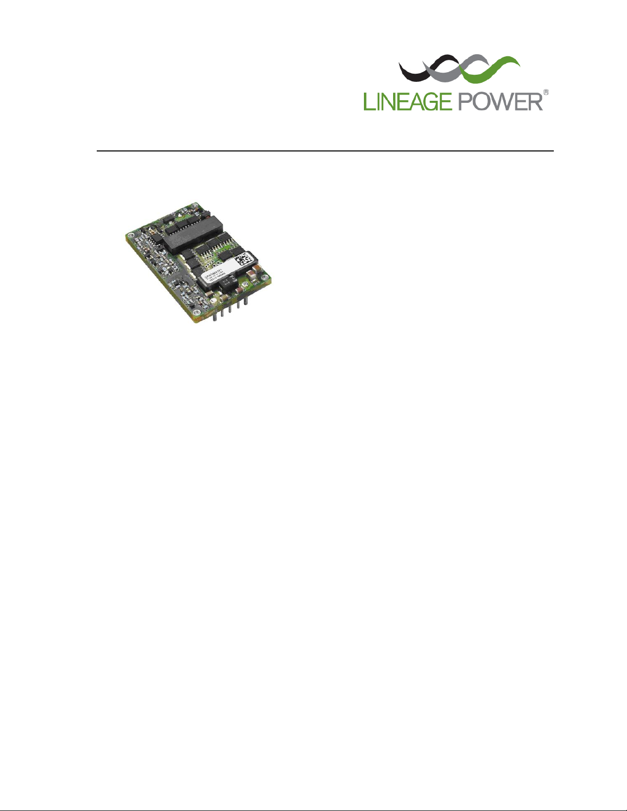
QPW050/060 Series DC-DC Converter Power Modules:
36-75Vdc Input; 1.2Vdc to 3.3Vdc Output; 50A/60A Output Current
RoHS Compliant
Applications
Distributed power architectures
Wireless Networks
Access and Optical Network Equipment
Enterprise Networks
Latest generation IC’s (DSP, FPGA, ASIC)
and Microprocessor powered applications
Options
Positive Remote On/Off logic
Case ground pin (-H Baseplate option)
Auto restart after fault shutdown
Features
Compliant to RoHS EU Directive 2002/95/EC (-Z
versions)
Compliant to ROHS EU Directive 2002/95/EC with lead
solder exemption (non-Z versions)
Delivers up to 60A output current
Improved Thermal Performance: 30A at 70ºC at 1m/s
(200LFM) for 3.3V
High power density: 119W/in
o
3
High efficiency – 93% at 3.3V full load
Low output voltage- supports migration to future IC
supply voltages down to 1.0V
Industry standard Quarter brick:
57.9 mm x 36.8 mm x 10.6 mm
(2.28 in x 1.45 in x 0.42 in)
Single tightly regulated output
2:1 input voltage range
Constant Switching frequency
Negative Remote On/Off logic
Output overcurrent/voltage/temperature protection
Output Voltage adjustment (±10%)
Wide operating temperature range (-40°C to 85°C)
Meets the voltage insulation requirements for
ETSI 300-132-2 and complies with and is licensed for
Basic Insulation rating per EN60950-1
CE mark meets 73/23/EEC and 93/68/EEC directives
UL* 60950-1, 2
60950-1-07 Certified, and VDE
nd
Ed. Recognized, CSA
‡
(EN60950-1, 2nd Ed.)
†
C22.2 No.
Licensed
ISO** 9001 certified manufacturing facilities
§
Description
The QPW-series dc-dc converters are a new generation of DC/DC power modules designed for maximum efficiency
and power density. The QPW series provide up to 60A output current in an industry standard quarter brick. The
converter incorporates synchronous rectification technology and innovative packaging techniques to achieve ultra
high efficiency reaching 93% at 3.3V full load. The ultra high efficiency of this converter leads to lower power
dissipation such that for most applications a heat sink is not required. The QPW series power modules are isolated
dc-dc converters that operate over a wide input voltage range of 36 to 75 Vdc and provide single precisely regulated
output. The output is fully isolated from the input, allowing versatile polarity configurations and grounding
connections
* UL is a re gistered trademark of Underwriters Laboratories, Inc.
†
CSA is a reg istered trademark of Canadian Standards Associat ion.
‡
VDE is a t rademark of Verband Deutscher Elektrotechniker e.V.
** ISO is a registered trademark of the International Orga nization of Standards
.
Document No: DS03-075 ver 1.16
PDF name: QPW Series.pdf
Page 2

Data Sheet
February 2, 2011
QPW050/060 Series Power Modules; DC-DC converters
36-75Vdc Input; 1.2Vdc to 3.3Vdc Output
Absolute Maximum Ratings
Stresses in excess of the absolute maximum ratings can cause permanent damage to the device. These are
absolute stress ratings only, functional operation of the device is not implied at these or any other conditions in
excess of those given in the operations sections of the data sheet. Exposure to absolute maximum ratings for
extended periods can adversely affect the device reliability.
Parameter Device Symbol Min Max Unit
Input Voltage
Continuous V
Transient (100ms) V
Operating Ambient Temperature All T
(see Thermal Considerations section)
Storage Temperature All T
I/O Isolation Voltage (100% factory Hi-Pot tested) All
IN
IN, trans
A
stg
-0.3 80 Vdc
-0.3 100 Vdc
-40 85 °C
-55 125 °C
1500 Vdc
Electrical Specifications
Unless otherwise indicated, specifications apply over all operating input voltage, resistive load, and temperature
conditions.
Parameter Device Symbol Min Typ Max Unit
Operating Input Voltage VIN 36 48 75 Vdc
Maximum Input Current I
(VIN=0V to 60V, IO=I
Inrush Transient All I2t 1 A2s
Input Reflected Ripple Current, peak-to-peak
(5Hz to 20MHz, 12μH source impedance; V
75V, I
= I
; see Figure 31)
O
Omax
Input Ripple Rejection (120Hz) All 50 dB
)
O, max
=0V to
IN
All 7 mAp-p
IN,max
CAUTION: This power module is not internally fused. An input line fuse must always be used.
This power module can be used in a wide variety of applications, ranging from simple standalone operation to an
integrated part of a sophisticated power architecture. To preserve maximum flexibility, internal fusing is not included,
however, to achieve maximum safety and system protection, always use an input line fuse. The safety agencies
require a fast-acting fuse with a maximum rating of 15A (see Safety Considerations section). Based on the
information provided in this data sheet on inrush energy and maximum dc input current, the same type of fuse with a
lower rating can be used. Refer to the fuse manufacturer’s data sheet for further information.
6 Adc
LINEAGE POWER 2
Page 3

Data Sheet
February 2, 2011
QPW050/060 Series Power Modules; DC-DC converters
36-75Vdc Input; 1.2Vdc to 3.3Vdc Output
Electrical Specifications (continued)
Parameter Device Symbol Min Typ Max Unit
3.36
2.55
1.83
1.53
1.22
3.40
2.57
1.86
1.56
1.25
Output Voltage Set-point
(V
IN=VIN,nom
, IO=I
, Tc =25°C)
O, max
Output Voltage
(Over all operating input voltage, resistive load, and
temperature conditions until end of life)
3.3V
2.5V
1.8V
1.5V
1.2V
3.3V
2.5V
1.8V
1.5V
1.2V
V
O, set
V
O
3.24
2.45
1.77
1.47
1.18
3.20
2.42
1.74
1.44
1.15
3.30
2.25
1.80
1.50
1.20
Output Regulation
Line (VIN=V
Load (IO=I
Temperature (Tc = -40ºC to +85ºC) All
IN, min
O, min
to V
to I
) All
IN, max
) All
O, max
0.05 0.2 %Vo
0.05 0.2 %Vo
15 50 mV
Output Ripple and Noise on nominal output
(VIN=V
RMS (5Hz to 20MHz bandwidth) All
Peak-to-Peak (5Hz to 20MHz bandwidth) All
External Capacitance 3.3V – 1.5V C
1.2V C
Output Current 3.3V I
Output Current Limit Inception 3.3V I
2.5V – 1.2V I
Efficiency
V
IN=VIN, nom
I
O=IO, max , VO
Switching Frequency f
and IO=I
IN, nom
, Tc=25°C
= V
O,set
to I
O, min
)
O, max
30 mV
100 mV
6,800 μF
22,000 μF
__
__
__
__
2.5V – 1.2V I
3.3V
2.5V
1.8V
1.5V
1.2V
O, max
O, max
o
o
O, lim
O, lim
η
η
η
η
η
sw
0 50 Adc
0 60 Adc
__
__
__
__
58
69
93
91
89
87
85
300
Dynamic Load Response
(Io/t=1A/10s; Vin=Vin,nom; Tc=25°C; Tested
with a 10 μF aluminum and a 1.0 μF ceramic
capacitor across the load.)
Load Change from Io= 50% to 75% of Io,max:
Peak Deviation
Settling Time (Vo<10% peak deviation)
Load Change from Io= 75% to 50% of Io,max:
Peak Deviation
Settling Time (Vo<10% peak deviation)
All
V
t
V
pk
ts
__ 4 __ %V
pk
s
__
4
200
200
__
s
%V
Isolation Specifications
V
V
Adc
Adc
%
%
%
%
%
kHz
s
dc
dc
rms
pk-pk
O, set
O, set
Parameter Symbol Min Typ Max Unit
Isolation Capacitance C
Isolation Resistance R
iso
iso
10
2700
pF
MΩ
General Specifications
Parameter Device Min Typ Max Unit
Calculated MTBF (IO=80% of I
airflow=1m/s(200LFM))
Weight
LINEAGE POWER 3
O, max
, Tc =40°C,
All 1,204,000 Hours
42 (1.48)
g (oz.)
Page 4

Data Sheet
February 2, 2011
QPW050/060 Series Power Modules; DC-DC converters
36-75Vdc Input; 1.2Vdc to 3.3Vdc Output
Feature Specifications
Unless otherwise indicated, specifications apply over all operating input voltage, resistive load, and temperature
conditions. See Feature Descriptions for additional information.
Parameter Device Symbol Min Typ Max Unit
Remote On/Off Signal Interface
(VIN=V
equivalent,
Signal referenced to V
Negative Logic: device code suffix “1”
Logic Low = module On, Logic High = module Off
Positive Logic: No device code suffix required
Logic Low = module Off, Logic High = module On
Logic Low Specification
Remote On/Off Current – Logic Low All I
On/Off Voltage:
Logic Low All V
Logic High – (Typ = Open Collector) All V
Logic High maximum allowable leakage current All I
Turn-On Delay and Rise Times
(IO=I
T
delay
application of Vin with Remote On/Off set to On
or operation of Remote On/Off from Off to On
with Vin already applied for at least one second.
T
90% of V
Output Voltage Adjustment
(See Feature Descriptions):
Output Voltage Set-point Adjustment Range (trim)
Output Overvoltage Protection
2.5V
1.8V
1.5V
1.2V
Overtemperature Protection
(See Feature Descriptions)
Input Undervoltage Lockout V
to V
IN, min
)
O, max
= Time until VO = 10% of V
; open collector or
IN, max
terminal)
IN-
from either
O,set
0.15 1.0 mA
1.2 V
__ 15 V
50 μA
2.5
12
3.3V
T
on/off
on/off
on/off
on/off
delay
T
0.0
rise
= time for VO to rise from 10% of V
rise
O,set
.
Output Voltage Remote-sense Range
O,set
to
2.5V – 1.2V
3.3V V
All T
Turn-on Threshold All
Turn-off Threshold All
T
delay
T
rise
V
sense
O, limit
ref
IN, UVLO
__
90
4.0
3.0
2.1
1.8
1.5
30 32
2.5
1.5
__
__
110
10
%V
110
%V
4.9 V
3.4 V
2.4 V
2.2 V
1.8 V
34.5 36 V
ms
ms
ms
ms
°C
V
o,nom
o,nom
LINEAGE POWER 4
Page 5
Data Sheet
February 2, 2011
QPW050/060 Series Power Modules; DC-DC converters
36-75Vdc Input; 1.2Vdc to 3.3Vdc Output
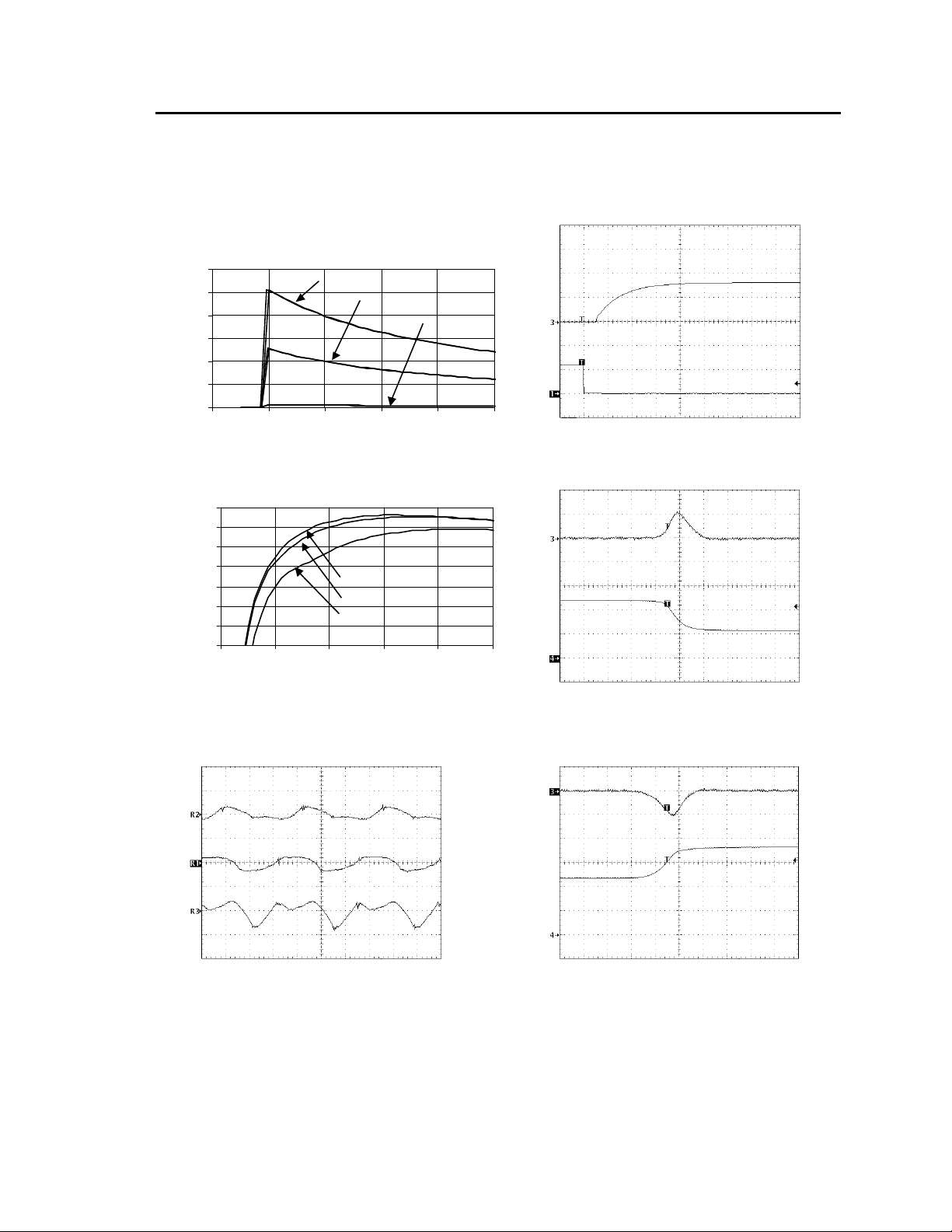
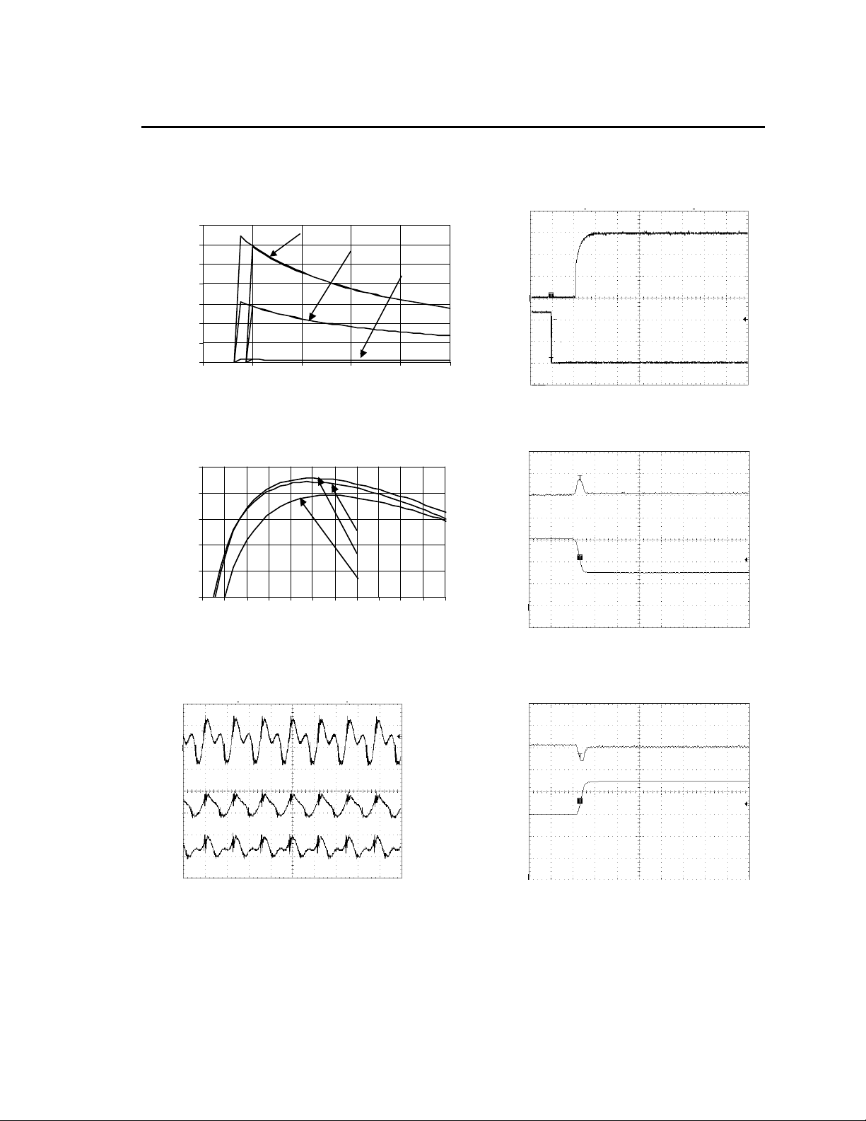
Characteristic Curves
The following figures provide typical characteristics for the QPW050A0F (3.3V, 50A) at 25ºC. The figures are identical
for either positive or negative Remote On/Off logic.
(A)
i
6
5
4
Io = 50 A
Io = 25 A
Io = 0 A
3
2
1
INPUT CURRENT, I
0
25 35 45 55 65 75
INPUT VOLTAGE, VO (V) TIME, t (5 ms/div)
Figure 1. Typical Input Characteristic at Room
Temperature.
94
92
90
88
86
84
82
80
EFFCIENCY, η (%)
Vi = 36 V
Vi = 48 V
Vi = 75 V
0 10203040 50
OUTPUT CURRENT, IO (A) TIME, t (100 μs/div)
Figure 2. Typical Converter Efficiency Vs. Output
current at Room Temperature.
(V) (2V/div)
ON/OFF
(V) (5V/div) V
O
V
OUTPUT VOLTAGE, On/Off VOLTAGE
Figure 4. Typical Start-Up Using Remote On/Off,
negative logic version shown.
(V) (100mV/div)
O
(A) (10A/div) V
O
OUTPUT CURRENT, OUTPUT VOLTAGE
I
Figure 5. Typical Transient Response to Step
change in Load from 50% to 25% of
Full Load at Room Temperature and 48
Vdc Input.
(V) (100mV/div)
O
(V) (50mV/div)
O
V
OUTPUT VOLTAGE,
(A) (10A/div) V
TIME, t (1s/div)
Figure 3. Typical Output Ripple and Noise at Room
Temperature and I
o
= I
o, max
.
O
OUTPUT CURRENT, OUTPUT VOLTAGE
I
Figure 6. Typical Transient Response to Step change
in Load from 50% to 75% of Full Load at Room
TIME, t (100 μs/div)
Temperature and 48 Vdc Input.
5
Page 6
Data Sheet
February 2, 2011
QPW050/060 Series Power Modules; DC-DC converters
36-75Vdc Input; 1.2Vdc to 3.3Vdc Output
Characteristic Curves
The following figures provide typical characteristics for the QPW060A0G (2.5V, 60A) at 25ºC. The figures are
identical for either positive or negative Remote On/Off logic.
6
5
(A)
i
4
3
2
1
0
25 35 45 55 65 75
INPUT CURRENT, I
INPUT VOLTAGE, VO (V) TIME, t (2.5 ms/div)
Figure 7. Typical Input Characteristic at Room
Temperature.
EFFCIENCY, η (%)
94
92
90
88
86
84
5 1015202530354045505560
OUTPUT CURRENT, IO (A) TIME, t (500 μs/div)
Figure 8. Typical Converter Efficiency Vs. Output
current at Room Temperature.
Io = 60A
Vi = 36 V
Vi = 48 V
Vi = 75 V
Io = 30 A
Io = 0 A
(V) (1V/div)
ON/OFF
(V) (5V/div) V
O
V
OUTPUT VOLTAGE, On/Off VOLTAGE
Figure 10. Typical Start-Up Using Remote On/Off,
negative logic version shown.
(V) (50mV/div)
O
(A) (10A/div) V
O
OUTPUT CURRENT, OUTPUT VOLTAGE
I
Figure 11. Typical Transient Response to Step
change in Load from 50% to 25%of Full Load at
Room Temperature and 48 Vdc Input.
75 Vin
(V) (50mV/div)
O
(V) (50mV/div)
O
V
OUTPUT VOLTAGE,
TIME, t (2.5s/div)
Figure 9. Typical Output Ripple and Noise at Room
Temperature and I
o
= I
o, max
.
(A) (10A/div) V
O
OUTPUT CURRENT, OUTPUT VOLTAGE
I
TIME, t (500 μs/div)
Figure 12. Typical Transient Response to Step change
in Load from 50% to 75% of Full Load at Room
Temperature and 48 Vdc Input.
LINEAGE POWER 6
Page 7
Data Sheet
February 2, 2011
QPW050/060 Series Power Modules; DC-DC converters
36-75Vdc Input; 1.2Vdc to 3.3Vdc Output
Characteristic Curves
The following figures provide typical characteristics for the QPW060A0Y (1.8V, 60A) at 25ºC. The figures are
identical for either positive or negative Remote On/Off logic.
4
3.5
(A)
i
3
2.5
2
1.5
1
0.5
0
25 35 45 55 65 75
INPUT CURRENT, I
INPUT VOLTAGE, VO (V) TIME, t (2.5 ms/div)
Figure 13. Typical Input Characteristic at Room
Temperature.
91
89
Io = 60 A
Io = 30 A
Io = 0 A
(V) (0.5V/div)
ON/OFF
(V) (5V/div) V
O
V
OUTPUT VOLTAGE On/Off VOLTAGE
Figure 16. Typical Start-Up Using Remote On/Off,
negative logic version shown.
87
85
83
EFFCIENCY, η (%)
81
Vi = 36 V
Vi = 48 V
Vi = 75 V
5 1015202530354045505560
OUTPUT CURRENT, IO (A) TIME, t (500 μs/div)
Figure 14. Typical Converter Efficiency Vs. Output
current at Room Temperature.
(V) (20mV/div)
O
V
OUTPUT VOLTAGE,
TIME, t (2.5s/div)
Figure 15. Typical Output Ripple and Noise at Room
Temperature and I
o
= I
o, max
.
(V) (50mV/div)
O
(A) (10A/div) V
O
OUTPUT CURRENT, OUTPUT VOLTAGE
I
Figure 17. Typical Transient Response to Step
change in Load from 50% to 25%of Full Load at
Room Temperature and 48 Vdc Input.
(V) (50mV/div)
O
(A) (10A/div) V
O
OUTPUT CURRENT, OUTPUT VOLTAGE
I
TIME, t (500 μs/div)
Figure 18. Typical Transient Response to Step change
in Load from 50% to 75% of Full Load at Room
Temperature and 48 Vdc Input.
LINEAGE POWER 7
Page 8
Data Sheet
February 2, 2011
QPW050/060 Series Power Modules; DC-DC converters
36-75Vdc Input; 1.2Vdc to 3.3Vdc Output
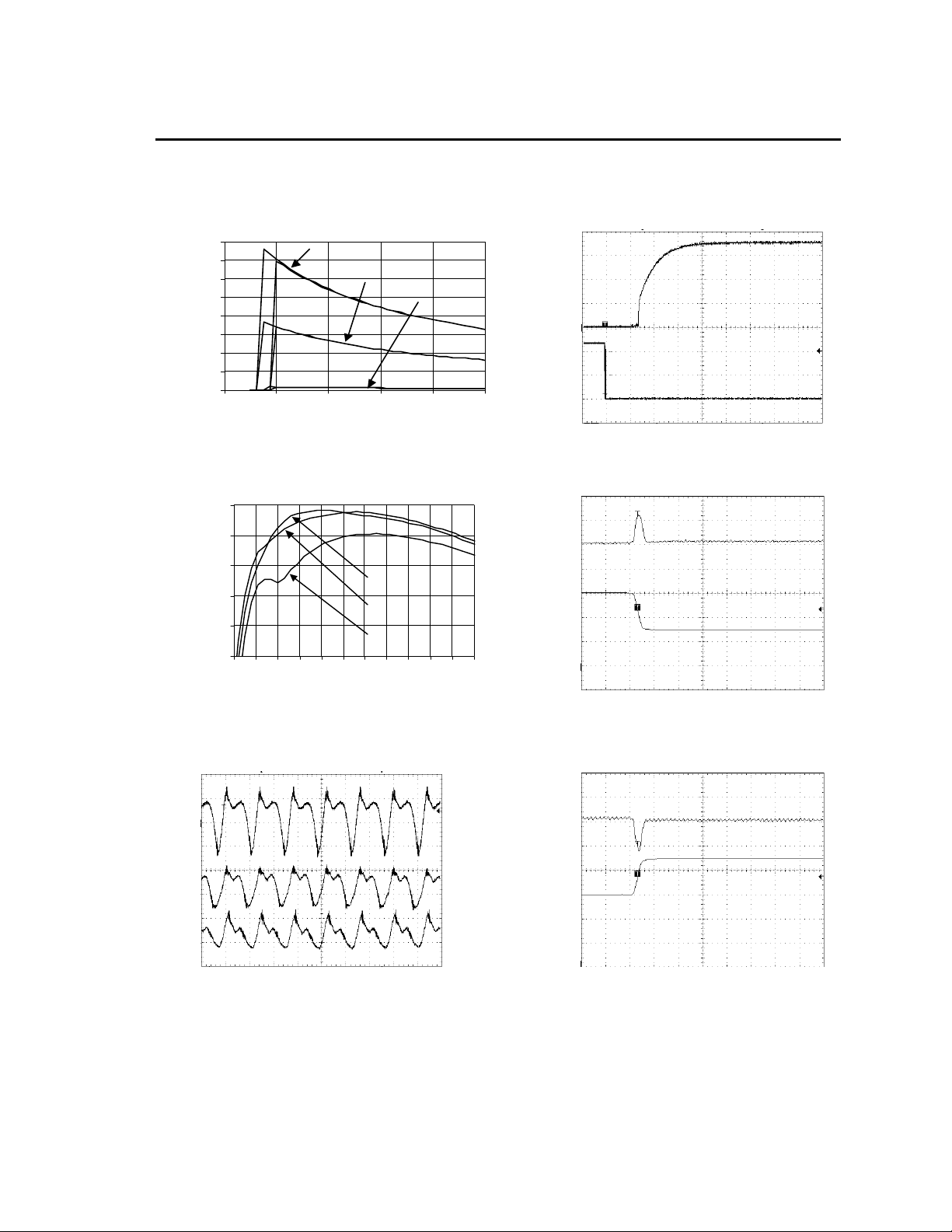
Characteristic Curves
The following figures provide typical characteristics for the QPW060A0M (1.5V, 60A) at 25ºC. The figures are
identical for either positive or negative Remote On/Off logic.
3.5
3
(A)
i
2.5
2
1.5
1
0.5
0
INPUT CURRENT, I
25 35 45 55 65 75
INPUT VOLTAGE, VO (V) TIME, t (2.5 ms/div)
Figure 19. Typical Input Characteristic at Room
Temperature.
91
89
Io = 60 A
Io = 3 0 A
Io = 0 A
(V) (0.5V/div)
ON/OFF
(V) (5V/div) V
O
V
OUTPUT VOLTAGE On/Off VOLTAGE
Figure 22. Typical Start-Up Using Remote On/Off,
negative logic version shown.
87
Vi = 36 V
85
83
EFFCIENCY, η (%)
81
Vi = 48 V
Vi = 75 V
5 1015202530354045505560
OUTPUT CURRENT, IO (A) TIME, t (500 μs/div)
Figure 20. Typical Converter Efficiency Vs. Output
current at Room Temperature.
(V) (20mV/div)
O
V
OUTPUT VOLTAGE,
TIME, t (2.5s/div)
Figure 21. Typical Output Ripple and Noise at Room
Temperature and I
o
= I
o, max
.
(V) (50mV/div)
O
(A) (10A/div) V
O
OUTPUT CURRENT, OUTPUT VOLTAGE
I
Figure 23. Typical Transient Response to Step
change in Load from 50% to 25%of Full Load at
Room Temperature and 48 Vdc Input.
(V) (50mV/div)
O
(A) (10A/div) V
O
OUTPUT CURRENT, OUTPUT VOLTAGE
I
TIME, t (500 μs/div)
Figure 24. Typical Transient Response to Step change
in Load from 50% to 75% of Full Load at Room
Temperature and 48 Vdc Input.
LINEAGE POWER 8
Page 9

Data Sheet
February 2, 2011
QPW050/060 Series Power Modules; DC-DC converters
36-75Vdc Input; 1.2Vdc to 3.3Vdc Output
Characteristic Curves
The following figures provide typical characteristics for the QPW060A0P (1.2V, 60A) at 25ºC. The figures are
identical for either positive or negative Remote On/Off logic.
3
(A)
i
2.5
2
1.5
1
0.5
0
INPUT CURRENT, I
25 35 45 55 65 75
INPUT VOLTAGE, VO (V) TIME, t (2.5 ms/div)
Figure 25. Typical Input Characteristic at Room
Temperature.
EFFCIENCY, η (%)
90
89
88
87
86
85
84
83
82
81
80
5 1015202530354045505560
OUTPUT CURRENT, IO (A) TIME, t (500 μs/div)
Figure 26. Typical Converter Efficiency Vs. Output
current at Room Temperature.
Io = 60 A
Io = 30 A
Vi = 36 V
Vi = 48 V
Vi = 75 V
Io = 0 A
(V) (0.5V/div)
ON/OFF
(V) (5V/div) V
O
V
OUTPUT VOLTAGE On/Off VOLTAGE
Figure 28. Typical Start-Up Using Remote On/Off,
negative logic version shown.
(V) (50mV/div)
O
(A) (10A/div) V
O
OUTPUT CURRENT, OUTPUT VOLTAGE
I
Figure 29. Typical Transient Response to Step
change in Load from 50% to 25%of Full Load at
Room Temperature and 48 Vdc Input.
(V) (50mV/div)
O
(V) (20mV/div)
O
V
OUTPUT VOLTAGE,
(A) (10A/div) V
TIME, t (2.5s/div)
Figure 27. Typical Output Ripple and Noise at Room
Temperature and I
o
= I
o, max
.
O
OUTPUT CURRENT, OUTPUT VOLTAGE
I
TIME, t (500 μs/div)
Figure 30. Typical Transient Response to Step change
in Load from 50% to 75% of Full Load at Room
Temperature and 48 Vdc Input.
LINEAGE POWER 9
Page 10

Data Sheet
February 2, 2011
QPW050/060 Series Power Modules; DC-DC converters
Test Configurations
Note: Measure input reflected-ripple current with a simulated
source inductance (LTEST) of 12 µH. Capacitor CS offsets
possible battery impedance. Measure current as shown
above.
Figure 31. Input Reflected Ripple Current Test
Setup.
Note: Use a 1.0 µF ceramic capacitor and a 10 µF aluminum
or tantalum capacitor. Scope measurement should be made
using a BNC socket. Position the load between 51 mm and
76 mm (2 in. and 3 in.) from the module.
Figure 32. Output Ripple and Noise Test Setup.
CONTACT AND
DISTRI BUTION LOSSES
O1
V
I
(+)
V
I
I
SUPPLY
V
I
(–)
V
CONTACT
RESISTANCE
Note: All measurements are taken at the module terminals.
When socketing, place Kelvin connections at module
terminals to avoid measurement errors due to socket contact
resistance.
Figure 33. Output Voltage and Effici en cy Test
Setup.
O
I
LOAD
O2
36-75Vdc Input; 1.2Vdc to 3.3Vdc Output
Design Considerations
Input Source Impedance
The power module should be connected to a low
ac-impedance source. A highly inductive source
impedance can affect the stability of the power
module. For the test configuration in Figure 31, a
100μF electrolytic capacitor (ESR<0.7 at 100kHz),
mounted close to the power module helps ensure the
stability of the unit. Consult the factory for further
application guidelines.
Output Capacitance
High output current transient rate of change (high
di/dt) loads may require high values of output
capacitance to supply the instantaneous energy
requirement to the load. To minimize the output
voltage transient drop during this transient, low E.S.R.
(equivalent series resistance) capacitors may be
required, since a high E.S.R. will produce a
correspondingly higher voltage drop during the
current transient.
Output capacitance and load impedance interact with
the power module’s output voltage regulation control
system and may produce an ’unstable’ output
condition for the required values of capacitance and
E.S.R.. Minimum and maximum values of output
capacitance and of the capacitor’s associated E.S.R.
may be dictated, depending on the module’s control
system.
The process of determining the acceptable values of
capacitance and E.S.R. is complex and is loaddependant. Lineage Power provides Web-based tools
to assist the power module end-user in appraising
and adjusting the effect of various load conditions and
output capacitances on specific power modules for
various load conditions.
Safety Considerations
For safety agency approval the power module must
be installed in compliance with the spacing and
separation requirements of the end-use safety agency
standards, i.e., UL 60950-1 2nd, CSA C22.2 No.
60950-1-07, DIN EN 60950-1:2006 + A11 (VDE0805
Teil 1 + A11):2009-11; EN 60950-1:2006 + A11:2009-
03. For the converter output to be considered meeting
the requirements of safety extra-low voltage (SELV),
the input must meet SELV requirements.
If the input source is non-SELV (ELV or a hazardous
voltage greater than 60 Vdc and less than or equal to
75Vdc), for the module’s output to be considered as
meeting the requirements for safety extra-low voltage
(SELV), all of the following must be true:
LINEAGE POWER 10
Page 11

Data Sheet
February 2, 2011
QPW050/060 Series Power Modules; DC-DC converters
36-75Vdc Input; 1.2Vdc to 3.3Vdc Output
Safety Considerations
The input source is to be provided with reinforced
insulation from any other hazardous voltages,
including the ac mains.
One V
The input pins of the module are not operator
Another SELV reliability test is conducted on the
Note: Do not ground either of the input pins of the
The power module has extra-low voltage (ELV)
outputs when all inputs are ELV.
For input voltages exceeding –60 Vdc but less than or
equal to –75 Vdc, these converters have been
evaluated to the applicable requirements of BASIC
INSULATION between secondary DC MAINS
DISTRIBUTION input (classified as TNV-2 in Europe)
and unearthed SELV outputs.
The input to these units is to be provided with a
maximum 15A fast-acting (or time-delay) fuse in the
unearthed lead.
pin and one V
IN
grounded, or both the input and output pins are
to be kept floating.
accessible.
whole system (combination of supply source and
subject module), as required by the safety
agencies, to verify that under a single fault,
hazardous voltages do not appear at the
module’s output.
module without grounding one of the output
pins. This may allow a non-SELV voltage to
appear between the output pins and ground.
(continued)
pin are to be
OUT
LINEAGE POWER 11
Page 12

Data Sheet
February 2, 2011
QPW050/060 Series Power Modules; DC-DC converters
Feature Descriptions
Overcurrent Protection
To provide protection in a fault output overload
condition, the module is equipped with internal
current-limiting circuitry and can endure current limit
for few seconds. If overcurrent persists for few
seconds, the module will shut down and remain latchoff. The overcurrent latch is reset by either cycling the
input power or by toggling the on/off pin for one
second. If the output overload condition still exists
when the module restarts, it will shut down again. This
operation will continue indefinitely until the
overcurrent condition is corrected.
An auto-restart option is also available.
Remote On/Off
Two remote on/off options are available. Positive logic
remote on/off turns the module on during a logic-high
voltage on the ON/OFF pin, and off during a logic low.
Negative logic remote on/off turns the module off
during a logic high and on during a logic low. Negative
logic, device code suffix "1," is the factory-preferred
configuration. To turn the power module on and off,
the user must supply a switch to control the voltage
between the on/off terminal and the VI (-) terminal
(Von/off). The switch can be an open collector or
equivalent (see Figure 34). A logic low is Von/off = 0
V to I.2 V. The maximum Ion/off during a logic low is 1
mA. The switch should maintain a logic-low voltage
while sinking 1 mA. During a logic high, the maximum
Von/off generated by the power module is 15 V. The
maximum allowable leakage current of the switch at
Von/off = 15V is 50 µA. If not using the remote on/off
feature, perform one of the following to turn the unit
on:
For negative logic, short ON/OFF pin to VI(-).
For positive logic: leave ON/OFF pin open.
Figure 34. Remote On/Off Implementation.
Remote Sense
Remote sense minimizes the effects of distribution
losses by regulating the voltage at the remote-sense
connections. The voltage between the remote-sense
pins and the output terminals must not exceed the
36-75Vdc Input; 1.2Vdc to 3.3Vdc Output
output voltage sense range given in the Feature
Specifications table i.e.:
[Vo(+) – Vo(-)] – [SENSE(+) – SENSE(-)] % of
V
.
o,nom
The voltage between the Vo(+) and Vo(-) terminals
must not exceed the minimum output overvoltage
shut-down value indicated in the Feature
Specifications table. This limit includes any increase
in voltage due to remote-sense compensation and
output voltage set-point adjustment (trim). See Figure
35. If not using the remote-sense feature to regulate
the output at the point of load, then connect
SENSE(+) to Vo(+) and SENSE(-) to Vo(-) at the
module.
Although the output voltage can be increased by both
the remote sense and by the trim, the maximum
increase for the output voltage is not the sum of both.
The maximum increase is the larger of either the
remote sense or the trim. The amount of power
delivered by the module is defined as the voltage at
the output terminals multiplied by the output current.
When using remote sense and trim: the output
voltage of the module can be increased, which at the
same output current would increase the power output
of the module. Care should be taken to ensure that
the maximum output power of the module remains at
or below the maximum rated power.
Figure 35. Effective Circuit Configuration for
Single-Module Remote-Sense Operation Output
Voltage.
Output Voltage Set-Point Adjustment (Trim)
Trimming allows the user to increase or decrease the
output voltage set point of a module. This is
accomplished by connecting an external resistor
between the TRIM pin and either the SENSE(+) or
SENSE(-) pins. The trim resistor should be positioned
close to the module.
If not using the trim feature, leave the TRIM pin open.
With an external resistor between the TRIM and
SENSE(-) pins (Radj-down), the output voltage set
point (Vo,adj) decreases (see Figure 36). The
following equation determines the required external
resistor value to obtain a percentage output voltage
change of %.
LINEAGE POWER 12
Page 13

Data Sheet
February 2, 2011
QPW050/060 Series Power Modules; DC-DC converters
36-75Vdc Input; 1.2Vdc to 3.3Vdc Output
Feature Description (continued)
Output Voltage Set-Point Adjustment (Trim)
For output voltages: 1.5V – 3.3V
510
KR downadj 2.10
%
For output voltage: 1.2V
KR downadj 49.33
%
Where,
VV
,
V
= Desired output voltage set point (V).
desired
With an external resistor connected between the
TRIM and SENSE(+) pins (Radj-up), the output
voltage set point (Vo,adj) increases (see Figure 37).
The following equation determines the required
external-resistor value to obtain a percentage output
voltage change of %.
For output voltages: 1.5V – 3.3V
upadj
K
R
desirednomo
,
nomo
V
nomo
,
V
For output voltage: 1.2V
V
R
upadj
K
,
Where,
V
= Desired output voltage set point (V).
desired
The voltage between the Vo(+) and Vo(-) terminals
must not exceed the minimum output overvoltage
shut-down value indicated in the Feature
Specifications table. This limit includes any increase
in voltage due to remote-sense compensation and
output voltage set-point adjustment (trim). See Figure
35.
Although the output voltage can be increased by both
the remote sense and by the trim, the maximum
increase for the output voltage is not the sum of both.
The maximum increase is the larger of either the
remote sense or the trim.
VV
,
nomo
V
1.1299
100%
510
%100**1.5
%*225.1
nomo
,
nomodesired
%100**769.9
%*6.0
100%
%
1.1299
%
2.10
49.33
The amount of power delivered by the module is
defined as the voltage at the output terminals
multiplied by the output current. When using remote
sense and trim, the output voltage of the module can
be increased, which at the same output current would
increase the power output of the module. Care should
be taken to ensure that the maximum output power of
the module remains at or below the maximum rated
power.
Figure 36. Circuit Configuration to Decrease
Output Voltage .
Figure 37. Circuit Configuration to Increase
Output Voltage.
Examples:
To trim down the output of a nominal 3.3V
module (QPW050A0F) to 3.1V
1.33.3
VV
%
∆% = 6.06
3.3
V
510
= 73.96 k
R
adj-down
To trim up the output of a nominal 3.3V module
(QPW050A0F) to 3.6V
%
3.3
V
100
100
KR downadj 2.10
06.6
3.36.3
VV
LINEAGE POWER 13
Page 14

Data Sheet
February 2, 2011
QPW050/060 Series Power Modules; DC-DC converters
Feature Description (continued)
Output Voltage Set-Point Adjustment (Trim)
Δ% = 9.1
6.2928
VV
%
Δ% = 5
R
tadj-up
28
V
KR upadj 936
10
= 11432 kΩ
KR upadj 2.10
R
= 98.47k
tadj-up
Output Over Voltage Protection
The output overvoltage protection consists of circuitry
that monitors the voltage on the output terminals. If
the voltage on the output terminals exceeds the over
voltage protection threshold, then the module will
shutdown and latch off. The overvoltage latch is reset
by either cycling the input power for one second or by
toggling the on/off signal for one second. The
protection mechanism is such that the unit can
continue in this condition until the fault is cleared.
Over Temperature Protection
These modules feature an overtemperature protection
circuit to safeguard against thermal damage. The
circuit shuts down and latches off the module when
the maximum device reference temperature is
exceeded. The module can be restarted by cycling
the dc input power for at least one second or by
toggling the remote on/off signal for at least one
second.
Input Under/Over Voltage Lockout
At input voltages below the input undervoltage lockout
limit, the module operation is disabled. The module
will begin to operate at an input voltage above the
undervoltage lockout turn-on threshold.
100
1036
5
1.9*225.1
510
1.9100*3.3*1.5
1.9
36-75Vdc Input; 1.2Vdc to 3.3Vdc Output
LINEAGE POWER 14
Page 15

Data Sheet
February 2, 2011
QPW050/060 Series Power Modules; DC-DC converters
36-75Vdc Input; 1.2Vdc to 3.3Vdc Output
Thermal Considerations without
Baseplate
The power modules operate in a variety of thermal
environments; however, sufficient cooling should be
provided to help ensure reliable operation.
Considerations include ambient temperature, airflow,
module power dissipation, and the need for increased
reliability. A reduction in the operating temperature of
the module will result in an increase in reliability. The
thermal data presented here is based on physical
measurements taken in a wind tunnel.
Heat-dissipating components are mounted on the top
side of the module. Heat is removed by conduction,
convection and radiation to the surrounding
environment. Proper cooling can be verified by
measuring the thermal reference
Peak temperature (T
) occurs at the position
ref
temperature (T
ref
).
indicated in Figures 38 - 40. For reliable operation this
temperature should not exceed listed temperature
threshold.
T
Figure 38.
Location for V
Figure 39.
Location for V
= 115ºC
ref
T
Temperature Measurement
ref
= 3.3V – 2.5V.
o
T
=110ºC
ref
T
Temperature Measurement
ref
= 1.8V.
o
Figure 40. T
ref
Location for V
Temperature Measurement
= 1.5V – 1.2V
o
T
ref
=115ºC
The output power of the module should not exceed
the rated power for the module as listed in the
Ordering Information table.
Although the maximum Tref temperature of the power
modules is 110 °C - 115 °C, you can limit this
temperature to a lower value for extremely high
reliability.
Heat Transfer via Convection
Increased airflow over the module enhances the heat
transfer via convection. Following derating figures
shows the maximum output current that can be
delivered by each module in the respective orientation
without exceeding the maximum T
versus local ambient temperature (T
convection through 2m/s (400 ft./min).
Note that the natural convection condition was
measured at 0.05 m/s to 0.1 m/s (10ft./min. to 20
ft./min.); however, systems in which these power
modules may be used typically generate natural
convection airflow rates of 0.3 m/s (60 ft./min.) due to
other heat dissipating components in the system. The
use of Figures 41 - 50 are shown in the following
example:
Example
What is the minimum airflow necessary for a
QPW050A0F operating at VI = 48 V, an output
current of 30A, and a maximum ambient temperature
of 70 °C in longitudinal orientation.
Solution:
Given: VI = 48V
Io = 30A
TA = 70 °C
Determine airflow (V) (Use Figure 41):
V = 1m/sec. (200ft./min.)
temperature
ref
) for natural
A
LINEAGE POWER 15
Page 16

Data Sheet
(
)
5
(
)
5
February 2, 2011
The following figures provide thermal derating characteristics.
QPW050/060 Series Power Modules; DC-DC converters
50
45
40
35
(A)
O
30
25
20
NATURAL CONVECTION
15
1.0 m/s (200 ft./min.)
10
2.0 m/s (400 ft./min.)
5
0
OUTPUT CURRENT, I
25 30 35 40 45 50 55 60 65 70 75 80 85
LOCAL AMBIENT TEMPERATURE, TA (C) LOCAL AMBIENT TEMPERATURE, TA (C)
Figure 41. Output Power Derating for QPW050A0F (Vo
= 3.3V) in Longitudinal Orientation with no baseplate;
Airflow Direction From Vin(–) to Vout(--); Vin = 48V.
50
40
(A)
O
30
20
NATURAL CONVECTION
10
0
OUTPUT CURRENT, I
25 30 35 40 45 50 55 60 65 70 75 80 8
Figure 42. Output Power Derating for QPW050A0F (Vo
= 3.3V) in Transverse Orientation with no baseplate;
Airflow Direction From Vin(–) to Vin(+); Vin = 48V.
1.0 m/s (200 ft./min.)
2.0 m/s (400 ft./min.)
LOCAL AMBIENT TEMPERATURE, TA (C) LOCAL AMBIENT TEMPERATURE, TA (C)
36-75Vdc Input; 1.2Vdc to 3.3Vdc Output
60
50
(A)
O
40
30
20
10
NATURAL
CONVECTION
1.0 m/s (200 ft./min.)
2.0 m/s
400 ft./min.
0
OUTPUT CURRENT, I
25 30 35 40 45 50 55 60 65 70 75 80 85
Figure 44. Output Power Derating for QPW060A0G (Vo
= 2.5V) in Transverse Orientation with no baseplate;
Airflow Direction From Vin(–) to Vin(+); Vin = 48V.
60
50
(A)
40
O
30
20
10
NATURAL
CONVECTION
1.0 m/s
2.0 m/s (400 ft./min.)
200 ft./min.
0
OUTPUT CURRENT, I
25 30 35 40 45 50 55 60 65 70 75 80 85
Figure 45. Output Power Derating for QPW060A0Y (Vo
= 1.8V) in Longitudinal Orientation with no baseplate;
Airflow Direction From Vin(–) to Vout(--); Vin = 48V.
60
50
(A)
O
40
NATURAL
30
CONVECTION
20
1.0 m/s (200 ft/min)
10
2.0 m/s (400 ft/min)
0
OUTPUT CURRENT, I
25 30 35 40 45 50 55 60 65 70 75 80 85
LOCAL AMBIENT TEMPERATURE, TA (C) LOCAL AMBIENT TEMPERATURE, TA (C)
Figure 43. Output Power Derating for QPW060A0G (Vo
= 2.5V) in Longitudinal Orientation with no baseplate;
Airflow Direction From Vin(–) to Vout(--); Vin = 48V.
60
50
(A)
O
40
30
20
10
OUTPUT CURRENT, I
Figure 46. Output Power Derating for QPW060A0Y (Vo
= 1.8V) in Transverse Orientation with no baseplate;
Airflow Direction From Vin(–) to Vin(+); Vin = 48V.
NATURAL
CONVECTION
1.0 m/s (200 ft./min.)
2.0 m/s (400 ft./min.)
0
25 30 35 40 45 50 55 60 65 70 75 80 8
LINEAGE POWER 16
Page 17

Data Sheet
February 2, 2011
The following figures provide thermal derating characteristics.
QPW050/060 Series Power Modules; DC-DC converters
60
50
(A)
O
40
30
20
10
0
OUTPUT CURRENT, I
NATURAL
CONVECTION
1.0 m/s (200 ft./min.)
2.0 m/s (400 ft./min.)
25 30 35 40 45 50 55 60 65 70 75 80 85
LOCAL AMBIENT TEMPERATURE, TA (C) LOCAL AMBIENT TEMPERATURE, TA (C)
Figure 47. Output Power Derating for QPW060A0M (Vo
= 1.5V) in Longitudinal Orientation with no baseplate;
Airflow Direction From Vin(–) to Vout(--); Vin = 48V.
60
50
(A)
40
O
30
NATURAL CONVECTION
20
1.0 m/s (200 ft./min.)
10
2.0 m/s (400 ft./min.)
0
25 30 35 40 45 50 55 60 65 70 75 80 85
OUTPUT CURRENT, I
36-75Vdc Input; 1.2Vdc to 3.3Vdc Output
60
50
(A)
O
40
30
NATURAL CONVECTION
20
1.0 m/s (200 ft./min.)
10
2.0 m/s (400 ft./min.)
0
OUTPUT CURRENT, I
25 30 35 40 45 50 55 60 65 70 75 80 85
Figure 50. Output Power Derating for QPW060A0P (Vo
= 1.2V) in Transverse Orientation with no baseplate;
Airflow Direction From Vin(–) to Vin(+); Vin = 48V.
Please refer to the Application Note “Thermal
Characterization Process For Open-Frame Board-Mounted
Power Modules” for a detailed discussion of thermal
aspects including maximum device temperatures.
LOCAL AMBIENT TEMPERATURE, TA (C)
Figure 48. Output Power Derating for QPW060A0M (Vo
= 1.5V) in Transverse Orientation with no baseplate;
Airflow Direction From Vin(–) to Vin(+); Vin = 48V.
60
50
(A)
O
40
30
NATURAL CONVECTION
20
1.0 m/s (200 ft./min.)
10
2.0 m/s (400 ft./min.)
0
OUTPUT CURRENT, I
25 30 35 40 45 50 55 60 65 70 75 80 85
LOCAL AMBIENT TEMPERATURE, TA (C)
Figure 49. Output Power Derating for QPW060A0P (Vo
= 1.2V) in Longitudinal Orientation with no baseplate;
Airflow Direction From Vin(–) to Vout(--); Vin = 48V.
LINEAGE POWER 17
Page 18

Data Sheet
February 2, 2011
QPW050/060 Series Power Modules; DC-DC converters
Thermal Considerations with
Baseplate
The baseplate option (-H) power modules are
constructed with baseplate on topside of the open
frame power module. The baseplate includes quarter
brick through-threaded, M3 x 0.5 mounting hole
pattern, which enable heat sinks or cold plates to
attaché to the module. The mounting torque must not
exceed 0.56 N-m (5 in.-lb.) during heat sink assembly.
This module operates in a variety of thermal
environments; however, sufficient cooling should be
provided to help ensure reliable operation.
Considerations include ambient temperature, airflow,
module power dissipation, and the need for increased
reliability. A reduction in the operating temperature of
the module will result in an increase in reliability. The
thermal data presented here is based on physical
measurements taken in a wind tunnel.
Heat-dissipating components are mounted on the
topside of the module and coupled to the baseplate
with thermal gap material. Heat is removed by
conduction, convection and radiation to the
surrounding environment. Proper cooling can be
verified by measuring the thermal reference
temperature (T
the position indicated in Figure 51. For reliable
operation this temperature should not exceed 95ºC
temperature threshold.
T
ref
Figure 51. T
Location for QPW-H baseplate option
The output power of the module should not exceed
the rated power for the module as listed in the
Ordering Information table.
Although the maximum Tref temperature of the power
modules is 95 °C, you can limit this temperature to a
lower value for extremely high reliability. Please refer
to the Application Note “Thermal Characterization
Process For Open-Frame Board-Mounted Power
). Peak temperature (T
ref
Temperature Measurement
ref
) occurs at
ref
36-75Vdc Input; 1.2Vdc to 3.3Vdc Output
Modules” for a detailed discussion of thermal aspects
including maximum device temperatures.
Heat Transfer via Convection
Increased airflow over the module enhances the heat
transfer via convection. Following derating figures
shows the maximum output current that can be
delivered by each module in the respective orientation
without exceeding the maximum T
versus local ambient temperature (T
convection through 2m/s (400 ft./min).
Note that the natural convection condition was
measured at 0.05 m/s to 0.1 m/s (10ft./min. to 20
ft./min.); however, systems in which these power
modules may be used typically generate natural
convection airflow rates of 0.3 m/s (60 ft./min.) due to
other heat dissipating components in the system. The
use of Figures 2 - 4 are shown in the following
example:
Example
What is the minimum airflow and heat sink size
necessary for a QPW050A0F-H operating at VI = 48
V, an output current of 30A, and a maximum ambient
temperature of 70 °C in transverse orientation.
Solution:
Given: VI = 48V
Io = 30A
TA = 70 °C
To determine airflow (V) and heatsink size (Use
Figures 52 - 53):
There are couple of solution can be derived from
below derating figures.
1) Baseplated with 0.25” heatsink in natural
convection (V= 0 m/sec) environment.
2) No baseplate required when operated with
airflow of 200 LFM (V = 1m/sec).
temperature
ref
) for natural
A
LINEAGE POWER 18
Page 19

Data Sheet
February 2, 2011
QPW050/060 Series Power Modules; DC-DC converters
The following figures provide thermal derating
characteristics.
55
(A)
50
O
45
40
35
30
Open frame
25
Baseplate
20
15
Baseplate w/ 0.25" heat sink
10
5
OUTPUT CURRENT, I
0
Baseplate w/ 0.5" heat sink
25 30 35 40 45 50 55 60 65 70 75 80 85
LOCAL AMBIENT TEMPERATURE, TA (C)
Figure 52. Output Power Derating for QPW050A0F
(Vo = 3.3V) in Transverse Orientation with baseplate
in natural convection environment; Airflow Direction
From Vin (–) to Vin (+); Vin = 48V
55
50
(A)
O
45
40
35
30
25
20
15
10
5
OUTPUT CURRENT, I
0
25 30 35 40 45 50 55 60 65 70 75 80 85
Open frame
Baseplate
Baseplate w/ 0.25" heat sink
Baseplate w/ 0.5" heat sink
LOCAL AMBIENT TEMPERATURE, TA (C)
Figure 53. Output Power Derating for QPW050A0F
(Vo = 3.3V) in Transverse Orientation with baseplate
in 200 LFM airflow environment; Airflow Direction
From Vin (–) to Vin (+); Vin = 48V
55
(A)
50
O
45
40
35
30
25
20
15
10
5
OUTPUT CURRENT, I
0
25 30 35 40 45 50 55 60 65 70 75 80 85
Open frame
Baseplate
Baseplate w/ 0.25" heat sin k
Baseplate w/ 0.5" heat sink
LOCAL AMBIENT TEMPERATURE, TA (C)
Figure 54. Output Power Derating for QPW050A0F
(Vo = 3.3V) in Transverse Orientation with baseplate
in 400 LFM airflow environment; Airflow Direction
From Vin (–) to Vin (+); Vin = 48V
36-75Vdc Input; 1.2Vdc to 3.3Vdc Output
LINEAGE POWER 19
Page 20

Data Sheet
February 2, 2011
QPW050/060 Series Power Modules; DC-DC converters
Layout Considerations
The QPW power module series are low profile in
order to be used in fine pitch system card
architectures. As such, component clearance
between the bottom of the power module and the
mounting board is limited. Avoid placing copper areas
on the outer layer directly underneath the power
module. Also avoid placing via interconnects
underneath the power module.
For additional layout guide-lines, refer to
FLTR100V10 data sheet.
Post solder Cleaning and Drying
Considerations
Post solder cleaning is usually the final circuit-board
assembly process prior to electrical board testing. The
result of inadequate cleaning and drying can affect
both the reliability of a power module and the
testability of the finished circuit-board assembly. For
guidance on appropriate soldering, cleaning and
drying procedures, refer to Lineage Power Board
Mounted Power Modules: Soldering and Cleaning
Application Note.
Through-Hole Lead-Free Soldering
Information
The RoHS-compliant through-hole products use the
SAC (Sn/Ag/Cu) Pb-free solder and RoHS-compliant
components. They are designed to be processed
through single or dual wave soldering machines. The
pins have an RoHS-compliant finish that is compatible
with both Pb and Pb-free wave soldering processes.
A maximum preheat rate of 3C/s is suggested. The
wave preheat process should be such that the
temperature of the power module board is kept below
210C. For Pb solder, the recommended pot
temperature is 260C, while the Pb-free solder pot is
270C max. Not all RoHS-compliant through-hole
products can be processed with paste-through-hole
Pb or Pb-free reflow process. If additional information
is needed, please consult with your Lineage Power
representative for more details.
36-75Vdc Input; 1.2Vdc to 3.3Vdc Output
LINEAGE POWER 20
Page 21

Data Sheet
February 2, 2011
QPW050/060 Series Power Modules; DC-DC converters
36-75Vdc Input; 1.2Vdc to 3.3Vdc Output
Mechanical Outline for Through-Hole Module without Baseplate Option
Dimensions are in millimeters and [inches].
Tolerances: x.x mm 0.5 mm [x.xx in. 0.02 in.] (Unless otherwise indicated)
x.xx mm 0.25 mm [x.xxx in 0.010 in.]
TOP
VIEW
SIDE
VIEW
BOTTOM
VIEW
*Top side label includes Lineage Power name, product designation, and data code.
LINEAGE POWER 21
Page 22

Data Sheet
February 2, 2011
QPW050/060 Series Power Modules; DC-DC converters
36-75Vdc Input; 1.2Vdc to 3.3Vdc Output
Mechanical Outline for Through-Hole Module with Baseplate Option
Dimensions are in millimeters and [inches].
Tolerances: x.x mm 0.5 mm [x.xx in. 0.02 in.] (Unless otherwise indicated)
x.xx mm 0.25 mm [x.xxx in 0.010 in.]
TOP
VIEW
SIDE
VIEW
BOTTOM
VIEW
*Bottom side label includes Lineage Power name, product designation, and data code.
LINEAGE POWER 22
Page 23

Data Sheet
February 2, 2011
QPW050/060 Series Power Modules; DC-DC converters
36-75Vdc Input; 1.2Vdc to 3.3Vdc Output
Recommended Pad Layout for Through Hole Module
Dimensions are in millimeters and (inches).
Tolerances: x.x mm 0.5 mm (x.xx in. 0.02 in.) [unless otherwise indicated]
x.xx mm 0.25 mm (x.xxx in 0.010 in.)
† - Option Feature, Pin is not present unless one of these options specified.
LINEAGE POWER 23
Page 24

Data Sheet
a
©
February 2, 2011
QPW050/060 Series Power Modules; DC-DC converters
36-75Vdc Input; 1.2Vdc to 3.3Vdc Output
Ordering Information
Please contact your Lineage Power Sales Representative for pricing, availability and optional features.
Table 1. Device Code
Product codes Input Voltage
Output
Voltage
QPW050A0F1 48V (36-75Vdc) 3.3V 50A 93% Through hole 108968686
QPW050A0F1Z 48V (36-75Vdc) 3.3V 50A 93% Through hole CC109113940
QPW050A0F41 48V (36-75Vdc) 3.3V 50A 93% Through hole 108986498
QPW050A0F41Z 48V (36-75Vdc) 3.3V 50A 93% Through hole CC109107190
QPW050A0F641Z 48V (36-75Vdc) 3.3V 50A 93% Through hole CC109163655
QPW050A0F1-HZ 48V (36-75Vdc) 3.3V 50A 93% Through hole CC109107182
QPW050A0F71-H 48V (36-75Vdc) 3.3V 50A 93% Through hole 108987207
QPW050A0F71-HZ 48V (36-75Vdc) 3.3V 50A 93% Through hole CC109107208
QPW050A0F41-HZ 48V (36-75Vdc) 3.3V 50A 93% Through hole CC109138483
QPW050A0F641-HZ 48V (36-75Vdc) 3.3V 50A 93% Through hole CC109135101
QPW060A0G1 48V (36-75Vdc) 2.5V 60A 91% Through hole 108982232
QPW060A0G1Z 48V (36-75Vdc) 2.5V 60A 91% Through hole CC109107216
QPW060A0G71-H 48V (36-75Vdc) 2.5V 60A 91% Through hole 108987215
QPW060A0G71-HZ 48V (36-75Vdc) 2.5V 60A 91% Through hole CC109107224
QPW060A0Y1 48V (36-75Vdc) 1.8V 60A 89% Through hole 108982265
QPW060A0M1 48V (36-75Vdc) 1.5V 60A 87% Through hole 108982240
QPW060A0M1Z 48V (36-75Vdc) 1.5V 60A 87% Through hole CC109114468
QPW060A0M1-HZ 48V (36-75Vdc) 1.5V 60A 87% Through hole CC109148846
QPW060A0P1 48V (36-75Vdc) 1.2V 60A 85% Through hole 108982257
QPW060A0P1Z 48V (36-75Vdc) 1.2V 60A 85% Through hole CC109113957
QPW060A0P41 48V (36-75Vdc) 1.2V 60A 85% Through hole CC109110533
QPW060A0P641 48V (36-75Vdc) 1.2V 60A 85% Through hole 108982380
QPW060A0P1-H 48V (36-75Vdc) 1.2V 60A 85% Through hole 108986506
Table 2. Device Options
Option Suffix
Negative remote on/off logic 1
Auto-restart 4
Pin Length: 3.68 mm ± 0.25mm (0.145 in. ± 0.010 in.) 6
Case Pin (only available with –H option) 7
Base Plate option -H
RoHS Compliant -Z
Output
Current
Efficiency
Connector
Type
Comcodes
Asia-Pacific Headquarters
Tel: +86.021.54279977*808
World Wide Headquarters
Lineage Power Corporation
601 Shiloh Road, Plano, TX 75074, USA
+1-888-LINEAGE(546-3243)
(Outside U.S.A.: +1-972-244-WATT(9288))
www.lineagepower.com
e-mail: techsupport1@lineagepower.com
Europe, Middle-East and Africa Headquarters
Tel: +49.89.878067-280
India Headquarters
Tel: +91.80.28411633
Lineage Power reserves the right to make changes to the product(s) or information contained herein without notice. No liability is assumed as a result of their use or
pplication. No rights under any patent accompany the sale of any such product(s) or information.
Lineage Power DC-DC products are protected under various patents. Information on these patents is available at www.lineagepower.com/patents.
2010 Lineage Power Corporation, (Plano, Texas) All International Rights Reserved.
Document No: DS03-075 ver 1.16
PDF name: QPW Series.pdf
 Loading...