

Page 1
GE
Data Sheet
June 20, 2013
©2013 General Electric Company. All rights reserved.
Features
-48V/10A Dual redundant input power distribution
3.3Vdc/3.6A & 5.0Vdc/150mA of isolated Management Power
for IPM or other housekeeping functions
Independent holdup capacitor charging voltage; trimmable
from 50 to 95Vdc for optimal real estate
OR’ing functionality, Inrush protection & hot swap capability
Integral EMI filter designed for the ATCA board to meet CISPR
Class B with minimal external filtering
Protection: Reverse polarity, under voltage, input transient
over voltage/current and temperature
I
2
C digital interface options
Isolated A/B Feed Loss /Open Fuse Alarm
High efficiency : 98%
-40 to 85ºC ambient temperature operation
Industry Standard Quarter brick size: 58.4 mm x 36.8 mm x
13.7 mm (2.3 in x 1.45 in x 0.54 in)
MTBF : 2,308,563 hours per TELCORDIA
ISO** 9001 & ISO 14001 certified manufacturing facilities
Compliant to RoHS II EU “Directive 2011/65/EU”
UL* 60950-1, 2nd Ed. Recognized, CSA† C22.2 No. 60950 1-07
Certified, and VDE‡ (EN60950-1, 2nd Ed.) Licensed
Meets the voltage and current requirements for ETSI 300-
132-2 and complies with and licensed for Basic insulation
rating per EN60950-1
2250 Vdc Isolation tested in compliance with IEEE 802.3
¤
PoE
standards
ISO**9001 and ISO 14001 certified manufacturing facilities
Applications
ATCA Front Board / Blade
Central Office Telecom equipment
High availability server and storage applications
Options
Choice of short pin lengths
I
2
C Digital Interface
Description
The PIM400 series of Power Input Modules are designed to greatly simplify the task of implementing dual redundant, hot swap –
48Vdc power distribution with EMI filtering on an ATCA or other telecom boards. The PIM400 with optional I2C digital interface
capability, when used with a variety of GE’s series of Bus converters (BarracudaTM Series) /POLs (DLynxTM Series) provides for a
quick, simple and elegant power solution to a wide variety of demanding & intelligent power system architectures.
* UL is a registered trademark of Underwriters Laboratories, Inc.
†
CSA is a registered trademark of Canadian Standards Association.
‡
VDE is a trademark of Verband Deutscher Elektrotechniker e.V.
** ISO is a registered trademark of the International Organization of Standards
¤ IEEE and 802 are registered trademarks of the Institute of Electrical and Electronics Engineers, Incorporated.
PIM400 Series; ATCA Board Power Input Modules
-36 to -75 Vdc; 400W/10A
Page 2
GE
Data Sheet
PIM400 Series; ATCA Board Power Input Modules
-36 to -75 Vdc; 400W/10A
June 20, 2013
©2013 General Electric Company. All rights reserved.
Page 2
External Holdup Capacitor Selection
External Holdup Trim Resistor Selection
Ref Des
Description
(Values)
Comments
F1-F4
Fuses (15A)
Max fuse rating not to exceed 20A, fast acting
F5,F6
Fuses (15A)
0.5 to 1A rated
R1,R2
Pre-charge Resistors (15 Ohms)
High Surge Power Type e.g. KOA P/N SG73
R_TRIM
Resistor
See Design Consideration section for details
R_PULLUP
Resistor (3.3 kOhms)
Alarm pull-up resistor
C_FLTR
Capacitor(s) (100F)
270 F (max)
C_HLDP
Capacitor(s)
3300F (max); see Design Consideration section for details
C_OUT
Capacitor(s)
Consult data sheet for the applicable DC/DC Bus Converter
C_EMI
Capacitors
See Design Consideration section for details
ATCA Board Typical Application
Suggested Bill of Materials
(Note: Customer is ultimately responsible for the final selection and verification of the suggested parts for the end application).
Page 3

GE
Data Sheet
PIM400 Series; ATCA Board Power Input Modules
-36 to -75 Vdc; 400W/10A
June 20, 2013
©2013 General Electric Company. All rights reserved.
Page 3
Parameter
Device
Symbol
Min
Typ
Max
Unit
Input Voltage
Continuous
All
VI
-0.5 -75
Vdc
Transient (Pulse duration = 1ms, square wave)
All
V
tr
-100
Vdc
Additionally: Transient Input Undervoltage,
Overvoltage and Impulse per ANSI T1.315-2001(R2006)
All
Reverse Polarity Protection
+75V
Vdc
Holdup Capacitor Voltage
Voltage (with respect to -48V_OUT)
All
V_HLDP
100
Vdc
Capacitance
All
C_HLDP
3300
F
Temperature
Normal Operating Ambient Temperature
(See Thermal Considerations section)
All
TA -40 85 oC
Storage Temperature
All
T
stg
-55 125 oC
Isolation Voltage
Input to MGMT_PWR Output Voltage & Alarm
All 2250
Vdc
Input to SHELF_GND Voltage
All 2250
Vdc
Input to LOGIC_GND Voltage
All 2250
Vdc
Absolute Maximum Ratings
Stresses in excess of the absolute maximum ratings can cause permanent damage to the device. These are absolute stress ratings
only, functional operation of the device is not implied at these or any other conditions in excess of those given in the operations
sections of the data sheet. Exposure to absolute maximum ratings for extended periods can adversely affect the device reliability.
CAUTION: This power module is not internally fused. Both A & B feeds and their corresponding returns must be
individually fused.
To preserve maximum flexibility, internal fusing is not included. However, to achieve maximum safety and system protection, the
safety agencies require a fast-acting fuse with a maximum rating of 20 Amps and Voltage Rating >/= 75Vdc for the –48AF, -48BF
VRTN_AF & VRTN_BF feeds. Consult Fusing and fault protection Section of PICMG 3.0 ATCA specifications for additional information.
Based on the information provided in this data sheet on inrush current and maximum dc input current, the same type of fuse with a
lower rating can be used. Refer to the fuse manufacturer’s data sheet for further information.
Page 4
GE
Data Sheet
PIM400 Series; ATCA Board Power Input Modules
-36 to -75 Vdc; 400W/10A
June 20, 2013
©2013 General Electric Company. All rights reserved.
Page 4
Parameter
Device
Symbol
Min
Typ
Max
Unit
-48V Dual Feed Inputs (-48_AF,-48_BF,VRTN_AF,VRTN_BF)
Input Voltage Range
All
VI
-36
-48
-75
Vdc
Output Current
With the following maximum power limits
400W @ 40Vin, 480W @ 48Vin, 540W @ 54Vin
All
II
10
Adc
Disabled input current drain if input voltage falls below V
UVLO
for > 2 seconds.
All
I
UVLO
10
mA
Enabled No-load input current
All
I
stdby
40
70
mA
Inrush Transient
(@ -48 VI, C_FLTR = 200F & EARLY_A, EARLY_B Pre-charge
resistors 15 ohms per leg as recommended in the “ ATCA
Board Typical Application” figure, p=2)
All
Duration: 0.1ms to 0.9ms
Ipk
40
Adc
Duration: 0.9ms to 3 ms
(Logarithmically declining)
Ipk
40 to 18
Adc
ENABLE A/B Signal Inputs (ENABLE_A, ENABLE_B)
Input Voltage Threshold (On/Off); Default Setting
All
V
UVHI
(On)
-33.5
-35.3
-36.0
Vdc
V
UVLO
(Off)
-32.4
-33.7
-34.1
Enable A / B Signals current drain (Vin = -48Vdc)
All
380
Adc
Main Output (-48V_OUT, VRTN_OUT)
Efficiency (Vin=-48V; 3,3V/5.0V @ no load)
400W Output Power
All η
98.2
%
300W Output Power
All η
98.5
%
Output Voltage Delay
All
T
delay
100
ms
Input Current Limit
All
I
limit
11
13
15
A
External Output Filter Capacitance (C_FLTR)
All
C_FLTR
80
100
270
F
Holdup Capacitor Output Voltage (V_HLDP)
Holdup Capacitor Voltage Trim Range
All
V_HLDP
50
90
95
V
Holdup Capacitor Output Voltage Tolerance @V_HLDP=90Vdc
+6 -6
%
-48V_OUT Threshold
To charge external holdup capacitors (C_HLDP)
40.0
To discharge external holdup capacitors (C_HLDP)
-34.5
-36.0
-37.5
dV/dt on Hold-up Connect
80
V/ms
Switching Frequency
f
330
kHz
A/B Feed Loss / Fuse Alarm Output (ALARM)
ALARM ON Input Voltage Threshold
All
-36.4
-37.2
-40.4
Vdc
ALARM OFF Input Voltage Threshold
-40.5
Vdc
External Pull-up Voltage
5.0
Vdc
Electrical Specifications
Unless otherwise indicated, specifications apply over all operating input voltage, resistive load, and temperature conditions.
Page 5
GE
Data Sheet
PIM400 Series; ATCA Board Power Input Modules
-36 to -75 Vdc; 400W/10A
June 20, 2013
©2013 General Electric Company. All rights reserved.
Page 5
Parameter
Output
Voltage
Symbol
Min
Typ
Max
Unit
+3.3V Isolated Management Power Output (+3V3)
Input Under-Voltage Lockout
All
-32.4
-33.7
-34.1
V
Turn-On Voltage Threshold
-34.5 V
Total Output Voltage Range
All
+3V3 3.170
3.350
3.430
V
(Over all operating input voltage, resistive Load and
temperature conditions until end of life).
Output Current
All
I O 0 ―
3.6
Adc
Output Ripple and Noise
All
Measured across 10F ceramic capacitor
VI = VI,nom TA = 25oC, Io = Io,max
RMS (500 MHz bandwidth)
―
16
30
mV
rms
Peak-to-peak (500MHz bandwidth)
― 75
100
mV
p-p
Output Current- Limit Inception
All
I
o,lim
― 4 6 A
rms
Output Short-circuit Current
All
I
o,sc
― 3 ― A
rms
External Load Capacitance
All
C
O,max
0 ―
1000
F
Switching Frequency
All
f
330
kHz
Dynamic Response
(di/dt =0.1A/μs, VIin= Vin,nom, TA=25°C)
Load change from IO = 50% to 75% of I
O, max,
Peak Deviation
Settling Time (VO<10% of peak deviation)
All
V
pk
t
s
7
800
%, V
O, set
s
Turn-On Delay
(Io = 80% of Io,max, TA=25°C)
All
T
delay
50 ms
Output voltage overshoot
(Io = 80% of Io,max, VI = 48Vdc TA=25°C)
All
3%
%, V
O, set
Output Over Voltage Protection
All
V
o, limit
3.7 5.4
V
+5.0V Isolated Management Power Output (+5V0)
Total Output Voltage Range
All
+5V0 4.80
5.00
5.20
V
(Over all operating input voltage, resistive Load and
temperature conditions until end of life).
Output Current
All
Io 0 ―
150
mAdc
Output Current-Limit Inception
All
I
o,lim
―
250 ― mA
Output Short-circuit Current
All
I
o,sc
― 150 ― mA
RMS
External Load Capacitance
All
C
O,max
0 ―
1000
F
Switching Frequency
All
f
―
330
―
kHz
Electrical Specifications (continued):
Page 6
GE
Data Sheet
PIM400 Series; ATCA Board Power Input Modules
-36 to -75 Vdc; 400W/10A
June 20, 2013
©2013 General Electric Company. All rights reserved.
Page 6
Parameter
Conditions
Symbol
Min
Typ
Max
Unit
Digital Signal Interface Characteristics
Clock frequency range
f
CLK
100
400
kHz
Measurement Tolerance
Feed Voltage A/B (-48V_AF & -48V_BF)
+/-3 %
Holdup Voltage (V_HLDP)
+/-3 %
-48V_OUT current (-48V_IOUT)
% of Io,max
+/-3 %
Module Temperature (TEMP)
+/-3
0C
Parameter
Device
Min
Typ
Max
Unit
Calculated MTBF (PO=0.8P
O, RATED
, 48VIN, TA=40°C, Airflow=300LFM)
Telecordia Issue 2 Method 1 Case 3
All 2,308,563
Hours
Weight
28.3 (1.0) g (oz.)
Digital Interface Specifications
Unless otherwise indicated, specifications apply over all operating input voltage, resistive load, and temperature conditions. See
Feature Descriptions for additional information.
General Specifications
Page 7

GE
Data Sheet
PIM400 Series; ATCA Board Power Input Modules
-36 to -75 Vdc; 400W/10A
June 20, 2013
©2013 General Electric Company. All rights reserved.
Page 7
INPUT CURRENT, OUTPUT VOLTAGE
I
IN
(A) (2Adiv) V
O
(V) (20V/div)
TIME, t (2ms/div)
TIME, t (200s/div)
Figure 1. Inrush Current
CH2: VRTN_OUT wrt -48Vout (Vo)
CH4: Input current (IIN)
Test Conditions:
48Vin, 400W, C_FLTR = 100uF
Fig 2: Input Transient on one feed
CH1: Feed B step to 60V (20V/Div)
CH2: Feed A at 48V (20V/Div)
CH3: VRTN_OUT (20V/Div)
Test Conditions:
Full load
TIME, t (2ms/div)
TIME, t (2ms/div)
Fig 3: Hold-up Event vs 3.3Vout
CH1: Feed A (20V/Div)
CH2: Hold-up Voltage (20V/Div)
CH3: VRTN_OUT (20V/Div)
CH4: 3.3Vout (2V/Div)
Test Conditions:
1. Payload Bus Converter: QBVW033A0B
2. Load: 12.0V Bus Converter Output @ 33A; 3.3V@3.6A
3. C_Hold-up = 2200 F
4. C_FLTR=220F
5. V_HLDP=90V
Fig 4: Hold-up Event vs 12.0Vout
CH1: Feed A (20V/Div)
CH2: Hold-up Voltage (20V/Div)
CH3: VRTN_OUT (20V/Div)
CH4: 12.0 Vout (5V/Div)
Test Conditions:
1. Payload Bus Converter: QBVW033A0B
2. Load: 12.0V Bus Converter Output @ 33A; 3.3V@3.6A
3. C_Hold-up = 2200 F
4. C_FLTR=220F
5. V_HLDP=90V
Characteristic Curves
The following figures provide typical characteristics for the PIM400X modules at 25ºC.
Page 8

GE
Data Sheet
PIM400 Series; ATCA Board Power Input Modules
-36 to -75 Vdc; 400W/10A
June 20, 2013
©2013 General Electric Company. All rights reserved.
Page 8
TIME, t (20ms/div)
TIME, t (10ms/div)
Fig 5: Turn-ON Threshold
CH1: Input Voltage (20V/Div)
CH2: VRTN_OUT voltage (20V/Div)
CH4: Input Current (5A/Div)
Fig 6: Turn-OFF Threshold
CH1: Input Voltage (20V/Div)
CH2: VRTN_OUT voltage (20V/Div)
CH4: Input Current (2A/Div)
-48V
IN
, +12.0V
(20Vdiv) (5V/div)
-48V
IN
, +3.3V
(20Vdiv) (5V/div)
TIME, t (10ms/div)
TIME, t (10ms/div)
Fig 7a: Line Transient performance per ANSI T1.315-2001
standard vs +12.0V output
CH1: +12Voutput voltage (5V/Div)
CH3: -48V input Voltage (20V/Div)
Test Conditions:
1. PIM400 + QBDW033A0 (12V Bus Converter)
2. Load: +12Vout @ 30A; 3.3V @ 3.0A
3. C_HLDP = 2200 F
4. C_FLTR) = 220 F
Fig 7b: Line Transient performance per ANSI T1.315-2001
standard vs 3.3V output
CH2: +3V3 Output Voltage (1V/Div)
CH3: -48V input Voltage (20V/Div)
Test Conditions:
5. PIM400 + QBDW033A0 (12V Bus Converter)
6. Load: +12Vout @ 30A; 3.3V @ 3.0A
7. C_HLDP = 2200 F
8. C_FLTR) = 220 F
Characteristic Curves (continued)
The following figures provide typical characteristics for the PIM400X modules at 25ºC.
Page 9

GE
Data Sheet
PIM400 Series; ATCA Board Power Input Modules
-36 to -75 Vdc; 400W/10A
June 20, 2013
©2013 General Electric Company. All rights reserved.
Page 9
EFFICIENCY, (%)
POWER DISSIPATION, (W)
OUTPUT CURRENT, IO (A)
Io1 = 0A
OUTPUT CURRENT, IO (A)
Io1 = 0A
Fig8a: Efficiency vs Output Current
Test Conditions:
No load on 3.3V output
Fig 8b: Power Dissipation vs Output Current
Test Conditions:
No load on 3.3V output
EFFICIENCY, (%)
POWER DISSIPATION, (W)
OUTPUT CURRENT, IO (A)
Io1 = 3.6A
OUTPUT CURRENT, IO (A)
Io1 = 3.6A
Fig 9a: Efficiency
Test Conditions:
Full load on 3.3V output
Fig 9b: Power Dissipation
Test Conditions:
Full load on 3.3V output
Characteristic Curves (continued)
The following figures provide typical characteristics for the PIM400X modules at 25ºC.
Page 10

GE
Data Sheet
PIM400 Series; ATCA Board Power Input Modules
-36 to -75 Vdc; 400W/10A
June 20, 2013
©2013 General Electric Company. All rights reserved.
Page 10
IOUT, +3.3Vo
(2A/div) (1V/div)
IOUT, +3.3Vo (ac)
(1A/div) (500mV/div)
TIME, t (0.500ms/div)
TIME, t (500s/div)
Fig 10: 3.3V Turn-On
Test Conditions:
Cout=10F ceramic
Fig 11: 3.3V Load Transient
Test Conditions:
Cout =10F ceramic
Step Load Change = 50%-75%-50% of I
out,max
Slew Rate = 1 A/s
OUTPUT VOLTAGE
V
O
(AC) (20mV/div)
ALARM OUTPUT INPUT VOLTAGE
V
ALARM
(2.0V/div) V
IN
(20V/div)
TIME, t (2s/div)
TIME, t (5ms/div)
Fig 12: 3.3V Ripple
Test Conditions:
Cout=10F ceramic
Iout=3.6A
Fig 13: ALARM Output change of state with input voltage
dropout
Characteristic Curves (continued)
The following figures provide typical characteristics for the PIM400X modules at 25ºC.
Page 11

GE
Preliminary Data Sheet
PIM400 Series; ATCA Board Power Input Modules
-36 to -75 Vdc; 400W/10A
June 20, 2013
©2013 General Electric Company. All rights reserved.
Page 11
Pin No.
Signal Name
Description
1
-48V_AF
-48V_A Feed (Externally Fused)
2
-48V_BF
-48V_B Feed (Externally Fused)
3
VRTN_AF
VRTN_A Feed (Externally Fused)
4
VRTN_BF
VRTN_B Feed (Externally Fused)
5
ENABLE_AF
ENABLE_A Feed (Externally Fused)
(Short Pin, connected to VRTN_A on the back plane)
6
ENABLE_BF
ENABLE_B Feed (Externally Fused)
(Short Pin, connected to VRTN_B on the back plane)
7
SHELF_GND
Shelf / Chassis / Safety Ground
8
+5V0
Isolated 5.0Vdc (Blue LED Power) w.r.t. LOGIC_GND
9
+3V3
Isolated 3.3Vdc (Management Power) w.r.t. LOGIC_GND
10*
ADD
I2C Address w.r.t. LOGIC_GND
11*
DAT
I2C Data w.r.t. LOGIC_GND
12*
CLK
I2C Clock w.r.t. LOGIC_GND
13
LOGIC_GND
Logic / Secondary / Isolated Ground
14
ALARM
Opto-isolated -48V A/B Feed Loss or Open Fuse Alarm (w.r.t LOGIC_GND)
15
-48V_OUT
OR’d and Inrush protected –48V Output Bus
16
TRIM_HLDP
Holdup capacitor output voltage trim w.r.t. -48V_OUT
17
VRTN_OUT
OR’d and Inrush protected VRTN Output Bus
18
V_HLDP
+ve terminal connection point for Holdup capacitor
PIM400 Internal Block Diagram
PIN FUNCTIONS
* Pins 10, 11 & 12 are present only on modules with I2C digital interface option (-K)
Page 12

GE
Data Sheet
PIM400 Series; ATCA Board Power Input Modules
-36 to -75 Vdc; 400W/10A
June 20, 2013
©2013 General Electric Company. All rights reserved.
Page 12
From
ATCA
(P10 Connector)
Connection
Requirement
To
PIM400X
Pin # Pin
Designation
Pin
#
Signal
Designation
33
-48V_A
Via Fuse(F3)
1
-48V_AF
34
-48V_B
Via Fuse(F4)
2
-48V_BF
28
VRTN_A
Via Fuse(F1)
3
VRTN_AF
29
VRTN_B
Via Fuse(F2)
4
VRTN_BF
30
EARLY_A
Via Resistor(R1) *
-48V_A
31
EARLY_B
Via Resistor(R2) *
-48V_B
32
ENABLE_A
Via Fuse(F5)
5
ENABLE_AF
27
ENABLE_B
Via Fuse(F6)
6
ENABLE_BF
25
SHELF_GND
Direct
7
SHELF_GND
26
LOGIC_GND
Direct
11
LOGIC_GND
From
PIM400X
To
ATCA Front Board
Notes
Pin # Pin
Designation
Terminal
Component
15
-48V_OUT
Vin(-)
DC/DC Converter
(1)
17
VRTN_OUT
Vin(+)
DC/DC Converter
18
V_HLDP
+ve
Holdup Capacitor
(2)
16
TRIM_HLDP
RTrim
Holdup Capacitor
8
+5V0
Management
Power
(3)
9
+3V3
14
ALARM
R
pull-up
IPM/System
Controller
(4)
From
PIM400KZ
To
ATCA Front Board
Notes
Pin # Pin
Designation
IPM/System Controller I2C
Interface
10
ADD
I2C Address w.r.t. LOGIC_GND
(5)
11
DAT
I2C Data w.r.t. LOGIC_GND
12
CLK
I2C Clock w.r.t. LOGIC_GND
Feature Descriptions
Introduction
The PIM400X module is designed to support the Advanced
Telecommunications Computing Architecture (ATCA) power
entry distribution requirements for the Front Board / Blade per
the PICMG 3.0 specifications.
The PICMG 3.0 specification defines the Mechanical, Shelf
Management Interface, Power Distribution, Thermal, Data I/O
and Regulatory requirements for the next generation of
modular telecom architecture platform for use in Central Office
telecom environments.
Input Pin Connections
The ATCA board is specified to accept up to a maximum of
400W of input power via dual, redundant -48Vdc Feeds
through the Zone 1 (Power and Management) connector,
designated P10.
The power connector provides board to backplane
engagement via pins of varying lengths. Please consult the
PICMG 3.0 specifications for details.
The following are the design considerations of the input pin
connections of the PIM400X to the ATCA power connector.
Output Pin Connections (Standard Module: PIM400Z)
The output pin connections of the PIM400X to the system board
are described below:
Additional Output Pin Connections (Modules with
optional I2C Digital Interface: Option - K)
The following additional output pins of the PIM400KZ available
for I2C Digital Interface to the IMP/System Controller are
defined below:
* Pre-charge resistors
The first pins to mate in the ATCA power connector are the
EARLY_A, EARLY_B, the two grounds (LOGIC_GND, SHELF_GND)
and the two returns (VRTN_A, VRTN_B); followed by staggered
connections of -48V_A and -48V_B power Feeds. The last pins
to engage are the two short pins, ENABLE_A & ENABLE_B. The
ATCA backplane connects the ENABLE_A to VRTN_A, ENABLE_B
to VRTN_B, EARLY_A to -48V_A and EARLY_B to -48V_B.
EARLY_A & EARLY_B Connections: During hot insertion of the
ATCA board, the Inrush Control circuit limits the surge current
to the C_FLTR capacitor. However, due to the presence of a
small amount of internal EMI filter capacitance (located before
the Inrush Control circuit), it is recommended that Precharge
resistors, R1 & R2 (100 Ohms, with appropriate surge capability)
be connected as shown in the Typical Application circuit.
Inrush Current Control / Hot Plug Functionality
The module provides inrush current control / hot plug
capability. The peak value of the inrush current and the
duration complies with the PICMG 3.0’s Inrush Transient
specifications. The specifications shall be met with the external
C_HLDP and C_FLTR capacitances as specified in the previous
sections.
The unique design of the module where the large energy
storage capacitors are segregated from the input filter
capacitors allows the module to meet the stringent PICMG’s
inrush transient specifications with minimal energy storage
capacitors.
Design Considerations
-48V Main Output Bus:
(Signal Names: -48V_OUT & VRTN_OUT)
This is the main -48V output bus that provides the payload
power to the downstream (one or more) DC/DC converters. The
Page 13

GE
Data Sheet
PIM400 Series; ATCA Board Power Input Modules
-36 to -75 Vdc; 400W/10A
June 20, 2013
©2013 General Electric Company. All rights reserved.
Page 13
Figure 14. Typical Class B EMC signature of PIM400F
as tested with GE’s bus converter, QBVW033A0B1
module.
PIM400X module does not regulate or provide isolation from
the input -48V A/B feeds.
The main functionality of the module is to provide -48V A/B
Feeds OR’ing, inrush protection for hot swap capability and EMI
filtering to attenuate the noise generated by the downstream
DC/DC converters.
The -48V_OUT pin connects to the Vin(-) pin and the
VRTN_OUT pin connects to the Vin(+) pin of the DC/DC
converter(s).
The -48V_OUT bus may require a fuse depending on
the power and fusing requirements of the DC/DC
converter.
Input filtering of the DC/DC converter is provided by
C_FLTR close to the input pins of the DC/DC
converter(s); additional high frequency decoupling
ceramic capacitors (0.01 to 0.1μF are recommended
for improved EMI performance.
The maximum C_FLTR capacitance across all the
downstream DC/DC converters should not exceed
270μF.
The minimum C_FLTR capacitance (80μF)
recommendation is based on meeting the EMI
requirements.
Holdup Capacitor Output Voltage (V_HLDP)
This output provides the user settable high voltage to charge
the C_HLDP capacitor(s) to allow the ATCA board to meet the
5ms, 0Volts transient requirements.
The V_HLDP pin connects to the +ve terminals of the
C_HLDP capacitors while the –ve terminals of the
C_HLDP connects to the -48V_OUT bus.
The C_HLDP capacitance is dependent on the system
power and the holdup time requirements based on
the following formula
Where T
drawn from the holdup capacitors (=input power of the
downstream DC/DC bus converter + Management Power),
V_HLDP is the trimmed holdup capacitor voltage and VUV is the
undervoltage lockout threshold of either the downstream bus
or the Management Power DC/DC converter (higher of the two).
is the desired holdup time, PHU is the holdup power
HU
Holdup Capacitor Trim Voltage (TRM_HLDP)
capacitance to less than -60Vdc and less than 20 joules within
one second of disconnection from the backplane.
Management Power (+3V3, +5V0)
Two isolated secondary output voltages (+3V3 & +5V0) are
provided for ATCA Front Board’s IPM/System Controller (3.3V)
and for the Blue LED’s (5.0V) power requirements. Both the
outputs are referenced to LOGIC_GND.
The management power is available even when the
input voltage is down to –36Vdc.
No additional output capacitors are required, but a
22μF tantalum/ceramic and a 0.01 to 0.1μF ceramic
capacitors are highly recommended to contain the
switching ripple and noise.
Input Fault Alarm Signal (ALARM)
Both the input feeds, -48V_AF & -48_BF are monitored via the 48V_ALARM signal. In the event of a loss of power from either
feeds (-48V_A or -48V_B) or the opening of their respective
fuses, the -48V_ALARM shall change its logical state indicating
a fault. During normal operation, the signal is Low. During fault
condition, the alarm signal shall assume a HI state when the
ALARM pin is pulled up to an external pull voltage (maximum
5.0V) via an external pullup resistor (R
internally referenced to the LOGIC_GND. A 3.3K pull up resistor
to 3.3V Management Power should suffice.
EMI Filtering
The module incorporates an EMI filter that is designed for the
ATCA board to help meet the conducted emissions
requirements of CISPR 22 Class B when used in conjunction
with GE’s DC/DC bus converters recommended for ATCA
applications.
The following Figure 14 depicts the Class B EMI performance of
PIM400F when tested with GE’s bus converter, QBVW033A0B1
with both modules mounted on the PIM400 Evaluation Board
together with additional high frequency EMI capacitors (Fig 15).
). The ALARM output is
Pullup
The resistor R_TRIM sets the external holdup capacitor voltage
to the desired setting. The output voltage is adjustable from 50
to 90V. The resistor, R_TRIM is selected by the following
equation:
High Voltage Discharge Mechanism:
Per the PICMG 3.0 specifications, the PIM400 provides an
internal discharge mechanism to discharge the holdup/bulk
Page 14

GE
Data Sheet
PIM400 Series; ATCA Board Power Input Modules
-36 to -75 Vdc; 400W/10A
June 20, 2013
©2013 General Electric Company. All rights reserved.
Page 14
Figure 15. PIM400 & QBVW033A0 Bus Converter Test
setup schematic
- 48V OUTPUT CURRENT (A)
AMBIENT TEMEPERATURE, TA (oC)
3.3V OUTPUT CURRENT, I
O
(A)
AMBIENT TEMEPERATURE, TA (oC)
AIRFLOW
For Safety and noise considerations, copper traces must not be
routed directly under the power module (PWB top layer). C_EMI
capacitors must make direct connections (preferably without
vias) to the bus converter (DC/DC) module pins with as much
copper width as possible. In case vias are necessary, allow for
multiple connections to the inner plane with vias placed outside
the footprint of the module. For additional layout guide-lines,
refer to GE’s FLT012A0Z Input Filter Module data sheet.
Safety Considerations
For safety-agency approval of the system in which the power
module is used, the power module must be installed in
compliance with the spacing and separation requirements of
the end-use safety agency standard, i.e. UL* 60950-1, 2nd Ed.
Recognized, CSA† C22.2 No. 60950-1-07 Certified, and VDE‡
(EN60950-1, 2nd Ed.) Licensed
The power input to these units is to be provided with a
maximum of fast acting 20A fuses with a voltage rating of at
least 75Vdc.
Refer to “Thermal Consideration” section for additional safety
considerations.
Thermal Considerations
The power modules operate in a variety of thermal
environments; however, sufficient cooling should be provided
to help ensure reliable operation.
Considerations include ambient temperature, airflow, module
power dissipation, and the need for increased reliability. A
reduction in the operating temperature of the module will result
in an increase in reliability. The thermal data presented here is
based on physical measurements taken in a wind tunnel.
The thermal reference point, T
shown in Figure 16. For reliable operation this temperature
should not exceed 130oC.
used in the specifications is
ref,
Figure 16. T
Temperature Measurement Location.
ref
Heat Transfer via Convection
Increased airflow over the module enhances the heat
transfer via convection. Derating curves showing the
maximum output current that can be delivered by
each module versus local ambient temperature (TA)
for natural convection and up to 2 m/s (400 lfm) forced airflow
are shown in Figures 17 & 18.
Please refer to the Application Note “Thermal Characterization
Process For Open-Frame Board-Mounted Power Modules” for a
detailed discussion of thermal aspects including maximum
device temperatures.
Figure 17. -48V Output Current Derating for the Module;
Airflow in the Transverse Direction from Pin7 to Pin1; Vin
=48V & 3.3V @ 1.5A.
Figure 18. 3.3V Output Current Derating for the Module;
Airflow in the Transverse Direction from Pin7 to Pin1; Vin
=48V & -48V Output current = 4A.
Page 15

GE
Data Sheet
PIM400 Series; ATCA Board Power Input Modules
-36 to -75 Vdc; 400W/10A
June 20, 2013
©2013 General Electric Company. All rights reserved.
Page 15
Time
Temp
Ramp up
max. 3°C/Sec
Ramp down
max. 4°C/Sec
Time Limited 90 Sec.
above 217°C
Preheat time
100-150 Sec.
Peak Temp. 240-245°C
25°C
150°C
200°C
217°C
Layout Considerations
The power modules are low profile in order to be used in fine
pitch system card architectures. As such, component
clearance between the bottom of the power module and the
mounting board is limited. Avoid placing copper areas on the
outer layer directly underneath the power module. Also avoid
placing via interconnects underneath the power module.
Particular attention should be paid to the clearance area as
noted in the Bottom View of the Mechanical Outline drawing.
For additional layout guidelines, refer to FLT012A0Z Data Sheet.
Process Considerations
Through-Hole Lead-Free Soldering Information
The RoHS-compliant, Z version, through-hole products use the
SAC (Sn/Ag/Cu) Pb-free solder and RoHS-compliant
components. The module is designed to be processed through
single or dual wave soldering machines. The pins have a RoHScompliant, pure tin finish that is compatible with both Pb and
Pb-free wave soldering processes. A maximum preheat rate of
3C/s is suggested. The wave preheat process should be such
that the temperature of the power module board is kept below
210C. For Pb solder, the recommended pot temperature is
260C, while the Pb-free solder pot is 270C max.
Reflow Lead-Free Soldering Information
The RoHS-compliant through-hole products can be processed
with paste-through-hole Pb or Pb-free reflow process.
Max. sustain temperature :
245C (J-STD-020C Table 4-2: Packaging Thickness>=2.5mm /
Volume > 2000mm3),
Peak temperature over 245C is not suggested due to the
potential reliability risk of components under continuous hightemperature.
Min. sustain duration above 217C : 90 seconds
Min. sustain duration above 180C : 150 seconds
Max. heat up rate: 3C/sec
Max. cool down rate: 4C/sec
In compliance with JEDEC J-STD-020C spec for 2 times reflow
requirement.
Pb-free Reflow Profile
Storage and Handling
The recommended storage environment and handling
procedures for moisture-sensitive surface mount packages is
detailed in J-STD-033 Rev. A (Handling,
Packing, Shipping and Use of Moisture/Reflow Sensitive Surface
Mount Devices). Moisture barrier bags (MBB) with desiccant are
required for MSL ratings of 2 or greater. These sealed
packages should not be broken until time of use. Once the
original package is broken, the floor life of the product at
conditions of 30°C and 60% relative humidity varies according
to the MSL rating (see J-STD-033A). The shelf life for dry packed
SMT packages will be a minimum of 12 months from the bag
seal date, when stored at the following conditions: < 40° C, <
90% relative humidity.
Figure 19. Recommended linear reflow profile using
Sn/Ag/Cu solder.
Post Solder Cleaning and Drying Considerations
Post solder cleaning is usually the final circuit-board assembly
process prior to electrical board testing. The result of
inadequate cleaning and drying can affect both the reliability of
a power module and the testability of the finished circuit-board
assembly. For guidance on appropriate soldering, cleaning and
drying procedures, refer to Lineage Power Board Mounted
Power Modules: Soldering and Cleaning Application Note
(AP01-056EPS).
For additional information, please contact your Sales
representative for more details.
BMP module will comply with J-STD-020 Rev. C
(Moisture/Reflow Sensitivity Classification for
Nonhermetic Solid State Surface Mount Devices) for both Pbfree solder profiles and MSL classification
procedures. BMP will comply with JEDEC J-STD-020C
specification for 3 times reflow requirement. The suggested Pbfree solder paste is Sn/Ag/Cu (SAC). The recommended linear
reflow profile using Sn/Ag/Cu solder is shown in Figure 19.
MSL Rating
The modules have a MSL rating of 2a.
Page 16

GE
Data Sheet
PIM400 Series; ATCA Board Power Input Modules
-36 to -75 Vdc; 400W/10A
June 20, 2013
©2013 General Electric Company. All rights reserved.
Page 16
8 bit Address
0101
xyz*
R/W
Digital Feature Descriptions
Full featured modules are available with I2C Digital Interface
(Option -K).
Modules with I2C capability monitor up to five analog
parameters and six status bits identified below in Tables 1and 2
respectively.
Modules with I2C Option Features:
Table 1: Internal register memory map
Address Structure:
7 bit Address + R/W bit
Four bits are fixed (0101), three bits (xyz) are variable, and the
least-significant bit is the read/write bit.
Table 3: Address structure
Address Selection:
The three bits (xyz) of the address are set with a single external
resistor from the ADD (pin10) to LOGIC_GND (pin 13). The 8
possible addresses are shown in Table 4 with the respective
resistance values.
Table 2: Digital signals
Note: Bit 0=LSB, Bit 7=MSB
I2C Command Structure:
The I2C is a 2-wire interface supporting multiple devices and
masters on a single bus. The connected devices can only pull
the bus wires low and they never drive the bus high. The bus
wires should be externally connected to a positive supply
voltage via a pull-up resistor. When the bus is idle, both DAT
and CLK are high.
Each device on the I2C bus is recognized by a unique address
stored in that device. Devices can be classified as masters or
slaves when performing data transfers. A master is a device
which initiates a data transfer on the bus and generates clock
signals to permit that transfer. At the same time, any device
addressed is considered slave. The PIM400 always acts as a
slave.
In PIM400 module, I2C interface is used for reporting critical
parameters like input voltage, output current, holdup capacitor
voltage and temperature data. The read protocol is shown in
the Fig 20 below.
Table 4: I2C Addressing
Fig 20: Typical I2C Read protocol
Page 17

GE
Data Sheet
PIM400 Series; ATCA Board Power Input Modules
-36 to -75 Vdc; 400W/10A
June 20, 2013
©2013 General Electric Company. All rights reserved.
Page 17
Mechanical Outline
Dimensions are in millimeters and (inches).
Tolerances: x.x mm 0.5 mm (x.xx in. 0.02 in.) [unless otherwise indicated]
x.xx mm 0.25 mm (x.xxx in 0.010 in.)
Page 18

GE
Data Sheet
PIM400 Series; ATCA Board Power Input Modules
-36 to -75 Vdc; 400W/10A
June 20, 2013
©2013 General Electric Company. All rights reserved.
Page 18
Pin No.
Signal Name
Pin No.
Signal Name
1
-48V_AF
10*
ADD
2
-48V_BF
11*
DAT
3
VRTN_AF
12*
CLK
4
VRTN_BF
13
LOGIC_GND
5
ENABLE_AF
14
ALARM
6
ENABLE_BF
15
-48V_OUT
7
SHELF_GND
16
TRIM_HLDP
8
+5V0
17
VRTN_OUT
9
+3V3
18
V_HLDP
Recommended Pad Layout
Dimensions are in millimeters and (inches).
Tolerances: x.x mm 0.5 mm (x.xx in. 0.02 in.) [unless otherwise indicated]
x.xx mm 0.25 mm (x.xxx in 0.010 in.)
NOTES:
1. FOR 0.030” X 0.025” RECTANGULAR PIN, USE 0.050” PLATED THROUGH HOLE
* Pins 10, 11 & 12 are present only on modules with I2C digital interface option (-K).
Page 19

GE
Data Sheet
PIM400 Series; ATCA Board Power Input Modules
-36 to -75 Vdc; 400W/10A
June 20, 2013
©2013 General Electric Company. All rights reserved.
Page 19
Packaging Details
The modules are supplied as standard in the plastic trays shown in Figure below.
Tray Specification
Material Antistatic coated PVC
Max surface resistivity 1012/sq
Color Clear
Capacity 12 power modules
Min order quantity 24 pcs (1 box of 2 full trays + 1 empty top tray)
Each tray contains a total of 12 power modules. The trays are self-stacking and each shipping box for the modules
will contain 2 full trays plus 1 empty hold down tray giving a total number of 24 power modules.
Notes:
1. All radius unspecified are R2.0mm
2. All angle unspecified are 50
3. Dimension unit: mm(L); A0(A).
Page 20

GE
Data Sheet
PIM400 Series; ATCA Board Power Input Modules
-36 to -75 Vdc; 400W/10A
Contact Us
For more information, call us at
USA/Canada:
+1 888 546 3243, or +1 972 244 9288
Asia-Pacific:
+86.021.54279977*808
Europe, Middle-East and Africa:
+49.89.878067-280
India:
+91.80.28411633
www.ge.com/powerelectronics
June 20, 2013
©2012 General Electric Company. All rights reserved.
Version 1.02
Input Voltage
Current
Rating
Auxiliary
Output #1
Auxiliary
Output #2
Options
Product codes
Comcodes
-36 to -75 Vdc
10A
3.3V/3.6A
5.0V/0.15A
-
PIM400Z
150019196
-36 to -75 Vdc
10A
3.3V/3.6A
5.0V/0.15A
I2C Digital Interface
PIM400KZ
150019197
-36 to -75 Vdc
10A
3.3V/3.6A
5.0V/0.15A
I2C Digital Interface & Short
pins (3.68mm)
PIM400K6Z
150033384
Option
Device Code Suffix
Short pins: 3.68mm ± 0.25mm (0.145 in. ± 0.010 in.)
6
Short pins: 2.79mm ± 0.25mm (0.110 in. ± 0.010 in.)
8
I2C Digital Interface
K
Description
Product Code
Comcode
PIM400 Evaluation Board
EVAL_PIM400
150030502
QBDW033A0B Series Power Modules; DC-DC Converters
36-75Vdc Input; 8.1-13.2Vdc Output; 33A Output Current
QBDW033A0B41Z
CC109159307
QBVW033A0B Series Power Modules; DC-DC Converters
36-75Vdc Input; 8.1-13.2Vdc Output; 33A Output Current
QBVW033A0B41Z
CC109165247
Ordering Information
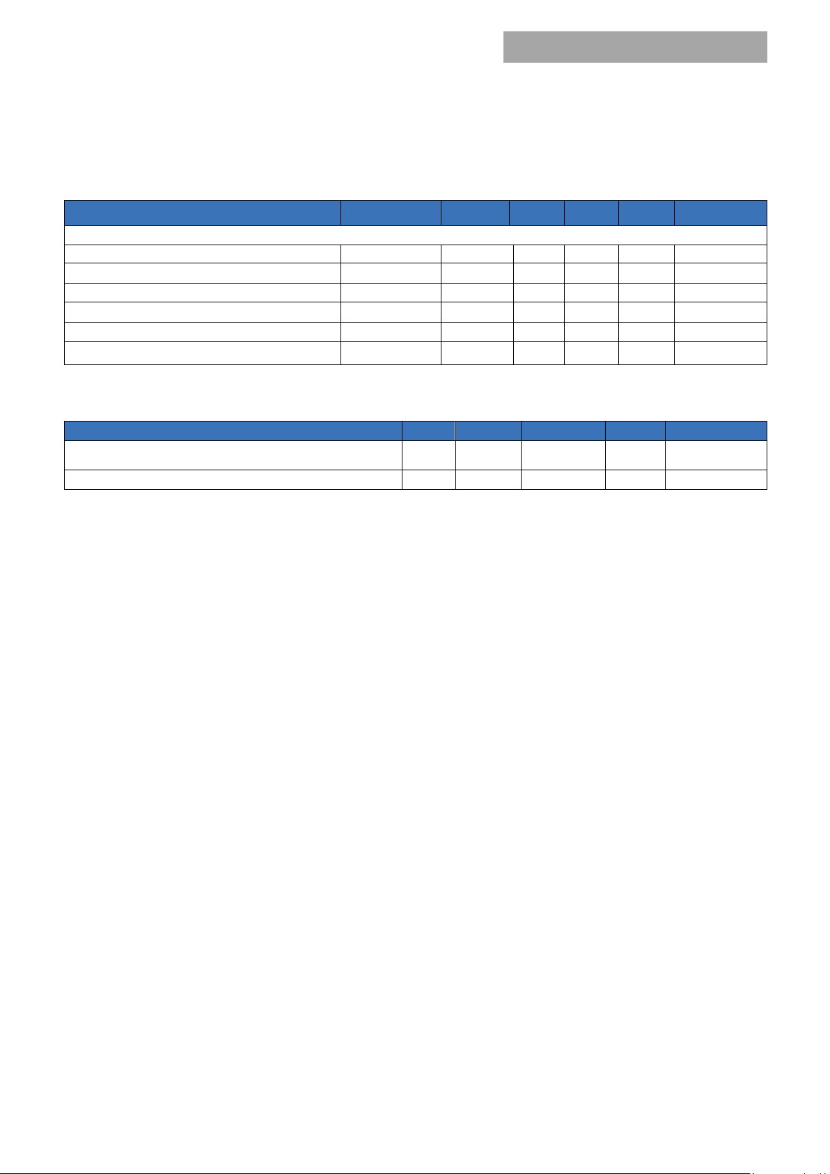
Please contact GE’s Sales Representative for pricing, availability and optional features.
Table 1. Device Code
Table 2. Device Options
Table 3. Related Products
 Loading...