

Page 1
Data Sheet
November 29, 2010
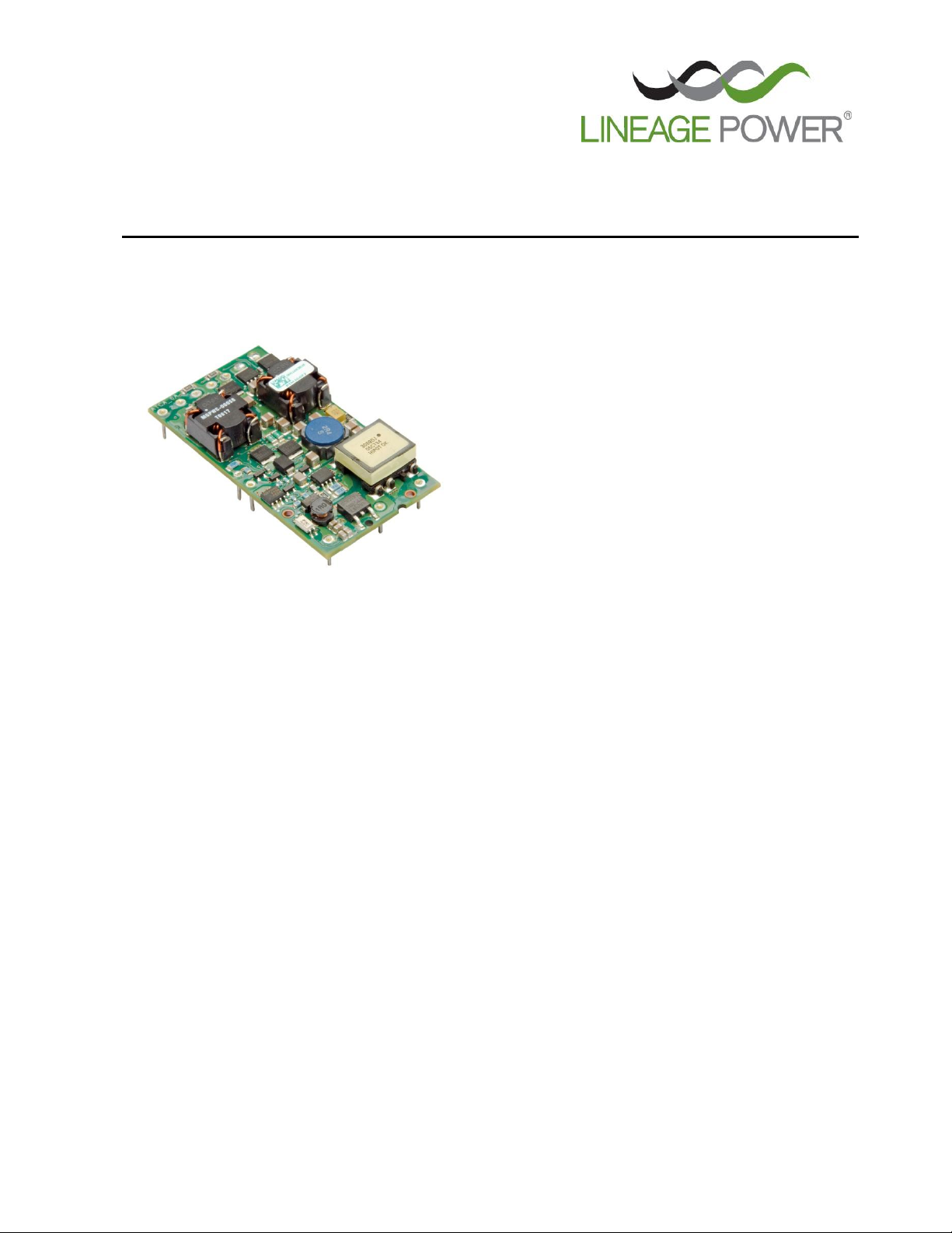
PIM300X Series; ATCA Board Power Input Modules
-38 to -75 Vdc; 300W Input
Document No: DS06-134 ver. 1.2
PDF name: pim300_series_ds.pdf
Features
300W / -48V telecom input power distribution
8W (3.3Vdc or 5.0Vdc) of isolated Management
Power for IPM or other housekeeping functions
OR’ing functionality for the A/B & RTN power feeds
as well as Enable A/B signals
Inrush protection / hot swap capability
Integral EMI filter designed for the ATCA board to
meet CISPR Class B
Independent 72Vdc output for charging the external
holdup capacitors resulting in significant board real
estate savings and bleed resistor power dissipation
A/B Feed Loss or open fuse alarm (opto-isolated)
Protection: Reverse polarity, under voltage, input
transient over voltage, over current & over
temperature
High efficiency : 98% @ –48V / 300W (@25C)
-5 to 85ºC ambient temperature operation
Compact design : 70.6 mm x 36.8 mm x 12.7 mm
(2.78 in x 1.45 in x 0.5 in)
MTBF : 1,362,480 hours per TELCORDIA
ISO** 9001 & ISO 14001 certified manufacturing
facilities
Compliant to RoHS EU Directive 2002/95/EC
UL* 60950-1 Recognized, CSA† C22.2 No. 60950-
1-03 Certified, EN 60950-1 (VDE‡ 0805: 2001-12)
Licensed , CE
Designed and tested for Basic Insulation (1500Vdc)
Applications
ATCA Front Board / Blade
Central Office Telecom equipment
High availability server and storage applications
Options
Choice of System Management Power:
3.3Vdc (PIM300F)
5.0Vdc (PIM300A)
Choice of short pin lengths
Description
The PIM300X-series is the higher power version of its highly successful predecessor, the PIM200X series. Besides
providing higher power over extended temperature range, the module is pin compatible and retains the same form
factor as the PIM200X series for ease of upgrading to higher power or thermally challenging ATCA board designs.
The PIM200X/300X series are a new class of power modules designed to greatly simplify the task of implementing
dual redundant, hot swap –48Vdc power distribution with EMI filtering on an ATCA or other telecom boards. The
PIM300X, when used with a variety of Lineage Power’s dc-dc converters/POLs provides for a quick, simple and
elegant power architecture solution to a wide variety of complex power requirements. While providing high reliability,
innovative features and compact design at a low cost, the module significantly reduces the valuable telecom board
real estate compared to conventional discrete designs. Besides processing the main –48V bus, the module greatly
simplifies the task of powering the IPM (for ATCA applications), system management or other housekeeping
functions by providing a completely isolated auxiliary 3.3V or 5.0V power bus.
RoHS Compliant
* UL is a registered trademark of Underwriters Laboratories, Inc.
†
CSA is a registered trademark of Canadian Standards Association.
‡
VDE is a trademark of Verband Deutscher Elektrotechniker e.V.
** ISO is a registered trademark of the International Organization of Standards
Page 2
Data Sheet
November 29, 2010
PIM300X Series; ATCA Board Power Input Modules
-38 to -75Vdc; 300W Input
Qty
Ref Des
Description
(Values)
MFR / PN
(or equivalent)
Comments
2
F1, F2
Fuse, SMT, 12 Amp
Bel Fuse: SSQ Series
Littelfuse 451/ 453 Series
(Voltage rating >/=75V)
VRTN_A, VRTN_B
2
F3, F4
Fuse, SMT, 10 Amp
-48V_A, -48V_B
2
F5, F6
Fuse, SMT, 1/16th Amp
ENABLE_A, ENABLE_B
2
C_FLTR
Capacitors, Al Electrolytic
100uF/100V
Nippon/Chemicon; KZE Series
Panasonic: FK Series (SMT)
Nichicon: UJ Series
C_FLTR(Max,Total) = 330 uF
4
C_HLDP
Capacitors, Al Electrolytic
470uF/80V
Nippon/Chemicon; KZE Series
Panasonic: FK Series (SMT)
C_HLDP(calculated)=1737 uF
(for 300W &Tholdup=9.3msecs)
OR
1
OR
Capacitors, Al Electrolytic
1800uF/80V
OR
Panasonic / ECEC1KP182DL
30mm(OD) X 20mm(L)
Snap-In Radial
1
R_Bleed
SM, 2.9Kohms, 1W
For C_HLDP=1800uF
2
C_EMI
SM, 4700pF, >/=1500V
Novacap, Murata or Syfer
Size: >/=1210
1
U1
300W/12V Bus Converter
Lineage Power: QBW025A0B1
1
U2
Opto-coupler (1500V)
Fairchild: HMHA2801
Safety approved
2
R1*, R2*
High Surge Power,
15 Ohms
KOA: SG73 (Size >/=1206)
*Optional; See “Design
Consideration” Section
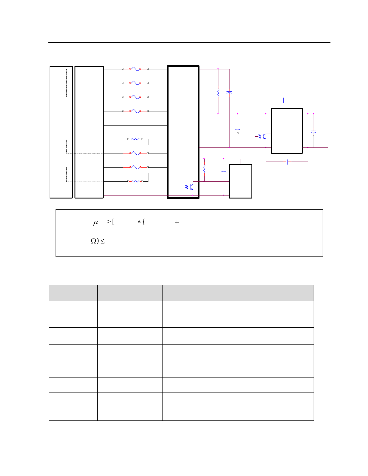
(29)
(25)
(30)
(28)
F1
F2
F3
F4
F5
F6
VRTN_A
ENABLE_A
ENABLE_B
-48V_B
EARLY_B
LOGIC_GND
SHELF_GND
EARLY_A
-48V_A
VRTN_B
Long Pin
Short Pin
Long Pin
ENABLE_BF
Short Pin
VRTN_AF
VRTN_BF
ENABLE_AF
-48V_AF
-48V_BF
R1
R2
(5)
(6)
(1)
(3)
(4)
(2)
(11)
(7)
(8)
R_Bleed
72V_CAP
C_HLDP
(13)
-48V_OUT
VRTN_OUT
MGMT_PWR
(10)
(9)
3K3
(12)
-48V_ALARM
22uF
ATCA
Zone 1
Connector
ATCA
Backplane
IPMC
Vcc
(System
Controller)
Enable
Payload Power
ON/OFF
Vin(-)
Vin(+)
PIM300X
Vo(-)
Vo(+)
C_EMI
C_EMI
LOGIC_GND
(Optional)
(Optional)
+12V_BUS
C_FLTR
(Bus Converter)
U1
U2
(32)
(27)
(26)
(33)
(34)
(31)
9.1/}]7.1)({)([)(_ msTWPFHLDPC holdupout
)(_/485.5)(_ FHLDPCBleedR
300W ATCA Board Typical Application
Suggested Bill of Materials
(Note: Customer is ultimately responsible for the selection and verification of the suggested parts).
LINEAGE POWER 2
Page 3

Data Sheet
November 29, 2010
PIM300X Series; ATCA Board Power Input Modules
-38 to -75Vdc ; 300W Input
Parameter
Device
Symbol
Min
Typ
Max
Unit
Input Voltage (Absolute values)
Continuous
All
VI 0 -48
-75
Vdc
Transient (Pulse duration above –75V = 1ms)
All
V
tr
-75 -100
Vdc
Temperature
Normal Operating Ambient Temperature
(See Thermal Considerations section)
All
TA -5 85 oC
Storage Temperature
All
T
stg
-55 125 oC
Power
Input Power, Maximum Allowable
All
P
in, max
300
W
Input to Output Voltage Differential
@ -48Vin & P
in,max
, TA=25 oC
All
V
delta
0.8V V
Efficiency
VIN=-48V, P
in,max
, TA=25 oC (MGMT_PWR=0W)
All η
98 %
Power Dissipation
(Internal Module Dissipation @ P
in, max
(with MGMT_PWR = 8W)
All
Pdiss
12 W
Output Power, Maximum Deliverable
(Management Power + Payload Power)
All
Pout
288 W
Management Power, Maximum Deliverable
(MGMT_PWR)
All
P
MGMT_PWR
8
W
Module Standby Power
(@-48Vin & MGMT_PWR=0W, Pout=0W)
All
P
Stdby
2.0 W
Isolation
Input to MGMT_PWR Output Voltage
All 1500
Vdc
Input to SHELF_GND Voltage
All 1500
Vdc
Input to LOGIC_GND Voltage
All 1500
Vdc
LOGIC_GND to SHELF_GND
Insulation Resistance with 100Vdc Test Voltage
All 9
MOhms
Absolute Maximum Ratings:
Stresses in excess of the absolute maximum ratings can cause permanent damage to the device. These are absolute
stress ratings only, functional operation of the device is not implied at these or any other conditions in excess of those
given in the operations sections of the data sheet. Exposure to absolute maximum ratings for extended periods can
adversely affect the device reliability.
CAUTION: This power module is not internally fused. Both A & B feeds and their corresponding
returns must be individually fused.
To preserve maximum flexibility, internal fusing is not included. However, to achieve maximum safety and system
protection, the safety agencies require a fast-acting fuse with a maximum rating of 15 Amps and Voltage Rating >/=
75Vdc for the –48AF, -48BF VRTN_AF & VRTN_BF feeds. Consult Fusing and fault protection (Section 4.1.4) of
PICMG 3.0 ATCA specifications for additional information. Based on the information provided in this data sheet on
inrush current and maximum dc input current, the same type of fuse with a lower rating can be used. Refer to the
fuse manufacturer’s data sheet for further information.
LINEAGE POWER 3
Page 4

Data Sheet
November 29, 2010
PIM300X Series; ATCA Board Power Input Modules
-38 to -75Vdc; 300W Input
Parameter
Device
Symbol
Min
Typ
Max
Unit
Main Input (-48_AF,-48_BF,VRTN_AF,VRTN_BF); (Absolute values)
Operating Input Voltage
(Module will operate down to –36V depending on
the output power and thermal environment but
may not support holdup time requirements)
All
VI
-38
-48
-75
Vdc
Input Voltage Turn-on Threshold
(Module On)
All
V
UVHI
-34.3
-35.3
-36.0
Vdc
Under Voltage Lockout Threshold
(Module Off)
All
V
UVLO
-32.4
-33.7
-34.1
Vdc
Maximum current drain if input voltage falls below
V
UVLO
for > 2 seconds.
All
I
stdby
10
mA
Maximum Input Current
(VI=0V to -75Vdc, Pin=P
in, max
)
All
I
I, max
9.0
Adc
Inrush Transient
(@ -48 VI and with C_FLTR = 200 F)
All
Ipk
20
(<50 s)
Adc
Duration: 0.1 to 0.9msecs (Per PICMG 3.0 specs.)
Ipk
44
Adc
Duration: 0.9 to 3 ms (Per PICMG 3.0 specs.)
(Logarithmically declining)
Ipk
44 to 18
Adc
Duration: 3 to 100ms (Per PICMG 3.0 specs.)
Ipk
6.25 8.8
Adc
ENABLE A/B Signal Inputs (ENABLE_A, ENABLE_B)
Enable A / B Signals current drain (Vin = -75Vdc)
All 700
Adc
Main Output (-48V_OUT, VRTN_OUT)
External Output Filter Capacitance (C_FLTR)
All
C_FLTR
200* 330
F
72V Holdup Capacitor Output (72V_CAP)
72V_CAP Output Voltage Tolerance
All
68.4
72.0
74.2
Vdc
72V_CAP ON (OR’d) Input Voltage Threshold
-36.2
-37.7
-39.2
Vdc
A/B Feed Loss / Fuse Alarm Output (-48V_ALARM)
-48V_ALARM is an Opto-isolated open collector
output with the emitter internally referenced to
LOGIC_GND.
Alarm Characteristics:
Power Good / Fuse Good = LO (Opto conducting)
A or B Feed Loss / Fuse (open) = HI (Opto off)
All
Alarm ON Input Voltage Threshold
-36.1
-37.2
-38.2
Vdc
Opto Transistor Collector to Emitter Voltage
Vceo
40
Vdc
Opto Transistor Collector to Emitter Dark Current
(Opto Diode current, Id = 0A)
Iceo
100
nA
Opto Transistor Collector Current
Ic
5
mA
Opto Transistor Collector Saturation Voltage
V
CE(sat)
0.3
Vdc
Electrical Specifications:
Unless otherwise indicated, specifications apply over all operating input voltage, resistive load, and temperature
conditions.
Note: * See “Design Considerations” section for further information.
LINEAGE POWER 4
Page 5

Data Sheet
November 29, 2010
PIM300X Series; ATCA Board Power Input Modules
-38 to -75Vdc; 300W Input
Parameter
Output
Voltage
Symbol
Min
Typ
Max
Unit
Management Power Output (MGMT_PWR)
Operating Input Voltage
3.3V/5.0V
VI -36
-48
-75
Vdc
Output Voltage Set-point
3.3V/5.0V
V
O, set
-2.0 ― +2.0
% V
O, set
(VI = -48Vdc, IO=I
O, max
, TA=25°C)
Output Voltage
3.3V/5.0V
VO -3.0
―
+3.0
% V
O, set
(Over all operating input voltage, resistive
Load and temperature conditions
until end of life)
Output Regulation
3.3V/5.0V
Line (VI= VI,min to VI,max)
―
0.05
0.2
%, V
O, set
Load (IO=I
O, min
to I
O, max
)
―
0.05
0.2
%, V
O, set
Temperature (TA = T
A,
min to T
A, max
)
― ―
1.00
%, V
O, set
Output Ripple and Noise
3.3V/5.0V
Measured across 22 F Tantalum/ceramic capacitor
VI = VI,nom TA = 25oC, Io = Io,max
RMS (5Hz to 20 MHz bandwidth)
― ― 25
mV
rms
Peak-to-peak (5Hz to 20MHz bandwidth)
― ― 75
mV
p-p
External Load Capacitance
3.3V/5.0V
C
O,max
0 ―
1000
F
Output Current
3.3V
5.0V
Io
Io 0 0 ― ―
2.4
1.6
Adc
Adc
Output Current-Limit Inception
3.3V
5.0V
Io,lim
Io,lim 3 2.5
―
―
Adc
Adc
Output Short-circuit Current (RMS)
3.3V
Io,sc ― 8 ― A
rms
5.0V
Io,sc ― 6 ― A
rms
Dynamic Response
(di/dt =0.1A/μs, VIin= VIn,nom, TA=25°C)
Load change from IO = 50% to 75% of I
O, max,
Peak Deviation
Settling Time (VO<10% of peak deviation)
3.3V/5.0V
V
pk
t
s
3
800
5
%, V
O, set
s
Turn-On Delay and Rise Times
(Io = 80% of Io,max, TA=25°C)
3.3V/5.0V
Tdelay 20
50
msec
Output voltage overshoot
(Io = 80% of Io,max, VI = 48Vdc TA=25°C)
3.3V/5.0V
3%
%, V
O, set
Output Over Voltage Protection
3.3V
5.0V
Vo, limit
3.7
5.6
5.4
7.0
V
Parameter
Min
Typ
Max
Unit
Calculated MTBF (Pin=80% of P
in, max
, TA=40°C, Vin=-48Vdc)
(Per Telcordia SR-332 Issue 1:Method 1 Case 3)
1,362,480
Hours
Weight 34 (1.2)
g (oz.)
Electrical Specifications (continued):
General Specifications
LINEAGE POWER 5
Page 6
Data Sheet
November 29, 2010
PIM300X Series; ATCA Board Power Input Modules
-38 to -75Vdc; 300W Input
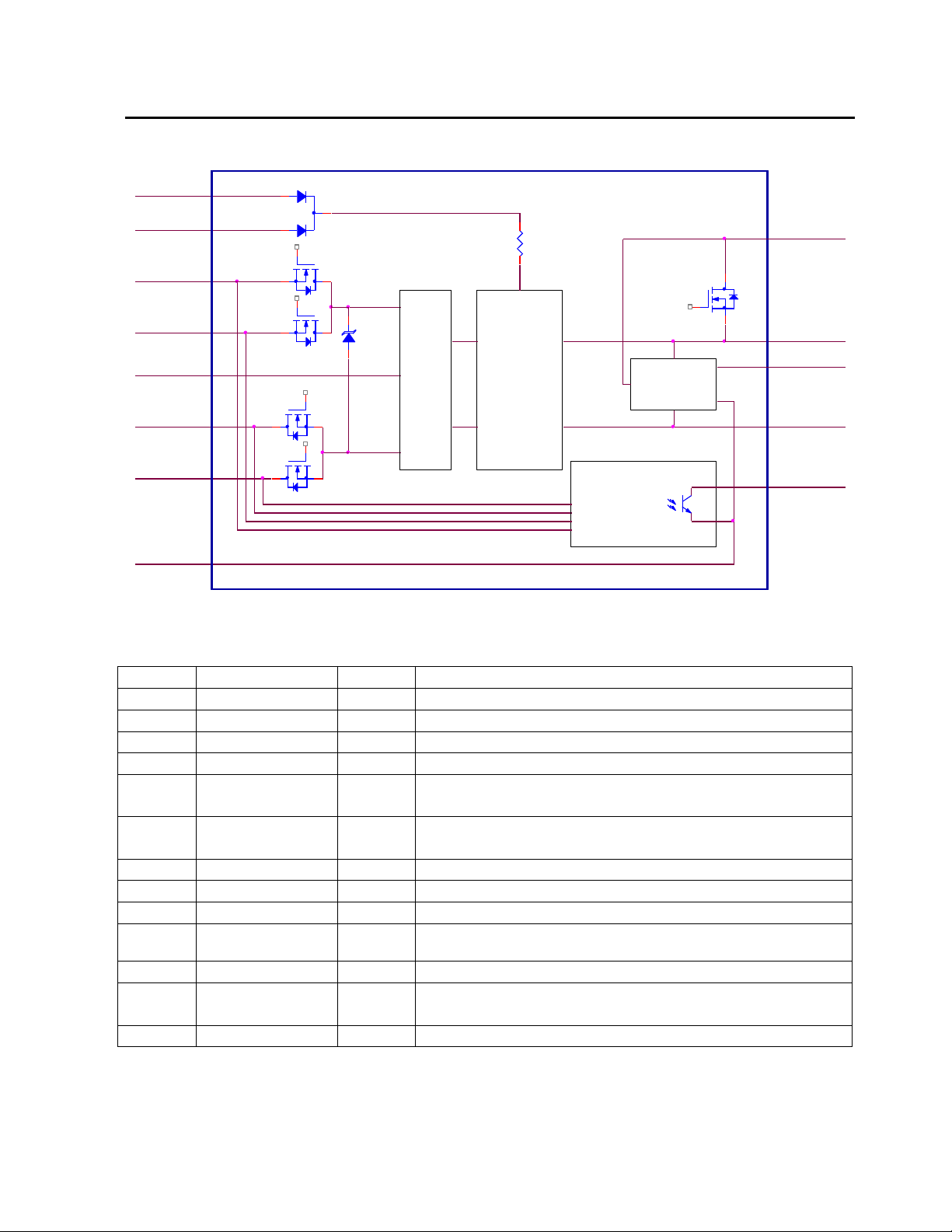
PIN NO.
PIN NAME
I/O
DESCRIPTION
1
-48_AF
I
-48V_A Feed (Externally Fused)
2
-48_BF
I
-48V_B Feed (Externally Fused)
3
VRTN_AF
I
VRTN_A Feed (Externally Fused)
4
VRTN_BF
I
VRTN_B Feed (Externally Fused)
5
ENABLE_AF
I
ENABLE_A Feed (Externally Fused)
(Short Pin, connected to VRTN_A on the back plane)
6
ENABLE_BF
I
ENABLE_B Feed (Externally Fused)
(Short Pin, connected to VRTN_B on the back plane)
7
SHELF_GND
I/O
Shelf / Chassis / Safety Ground
8
72V_CAP
O
Holdup/Bulk capacitor output voltage
9
-48V_OUT
O
OR’d and Inrush Protected –48V Output Bus
10
MGMT_PWR
O
3.3V / 5.0V Isolated Management Power Output ( w.r.t
LOGIC_GND)
11
LOGIC_GND
I/O
Logic / Secondary / Isolated Ground
12
-48V_ALARM
O
Opto-isolated -48V A/B Feed Loss or Open Fuse Alarm
(w.r.t LOGIC_GND)
13
VRTN_OUT
O
OR’d and Inrush Protected VRTN Output Bus
(5)
(6)
(3)
(4)
(7)
(1)
(2)
(11)
(8)
(13)
(10)
(9)
(12)
VRTN_OR
DC/DC
CONVERTER
-48_OR
INRUSH
PROTECTION
+48OUT
-48OUT
EMI
FILTER
Normally=OFF
Power Loss=ON
Alarms
&
Monitoring
VRTN_OUT
-48V_OUT
-48V_ALARM
MGMT_PWR
ENABLE_AF
ENABLE_BF
VRTN_AF
VRTN_BF
SHELF_GND
-48_AF
-48_BF
LOGIC_GND
72V_CAP
PIM300X Internal Block Diagram
PIN FUNCTIONS
LINEAGE POWER 6
Page 7

Data Sheet
November 29, 2010
PIM300X Series; ATCA Board Power Input Modules
-38 to -75Vdc; 300W Input
Figure 1. Inrush Current
CH1: -48_AF, CH2: -48V_OUT,
CH4: Iin(-48_AF)
Test Conditions:
-48_AF=-48Vdc, -48V_BF=0Vdc
PIM300F @ Max Load (Pin=300W)
C_FLTR=200μF, C_HLDP=4X470μF
Figure 2. Inrush Current
(Expanded view of the first surge current)
CH1: -48_AF, CH2: -48V_OUT,
CH4: Iin(-48_AF)
Test Conditions:
-48_AF=-48Vdc, -48V_BF=0Vdc
PIM300F @ Max Load (Pin=300W)
C_FLTR=200μF, C_HLDP=4X470μF
Figure 3. Power Up into Shorted Output
CH1: -48_AF, CH3: -48V_OUT,
CH2: Iin(-48_AF)
Test Conditions:
-48_AF=-48Vdc, -48V_BF=0Vdc
PIM300F @ No Load
C_FLTR=200μF, C_HLDP=4X470μF
Figure 4. OR’ing Functionality when Feed B is
shorted
CH1: -48V_OUT(AC), CH2: Iin(-48_AF)
CH3: Iin(-48_BF), CH4: 3.3V Output
Test Conditions:
-48_AF=-48Vdc, -48V_BF=-50Vdc
I(-48V_OUT) = 1A
C_FLTR=200μF, C_HLDP=4X470μF
Characteristic Curves
The following figures provide typical characteristics for the PIM300X modules at 25ºC.
LINEAGE POWER 7
Page 8

Data Sheet
November 29, 2010
PIM300X Series; ATCA Board Power Input Modules
-38 to -75Vdc; 300W Input
Figure 5. Input Voltage Turn-On Threshold
CH1: -48_AF, CH2: -48V_OUT,
CH4: Iin(-48_AF)
Test Conditions:
-48_AF=-48Vdc, -48V_BF=0Vdc
I(-48V_OUT)=1A, I(MGMT_PWR)=0A
C_FLTR=200μF, C_HLDP=0μF
Figure 6. Input Voltage Turn-Off Threshold
CH1: -48_AF, CH2: -48V_OUT,
CH4: Iin(-48_AF)
Test Conditions:
-48_AF=-48Vdc, -48V_BF=0Vdc
I(-48V_OUT)=1A, I(MGMT_PWR)=0A
C_FLTR=200μF, C_HLDP=0μF
Figure 7. Loss of Feed A; Switchover to Feed B
CH1: MGMT_PWR, CH2: -48V_OUT,
CH3: Iin(-48_AF), CH4: Iin(-48V_BF)
Test Conditions:
1. Feed A (-48V_AF=60V) > Feed B (-48V_BF=48V)
2. Fast Loss of Feed A; Switchover to Feed B
3. PIM300F @ Max Load (Pin=300W)
4. C_FLTR=200μF, C_HLDP=4X470μF
Figure 8. Holdup Performance; Loss of
Feed A (with Feed B=0Vdc); Load=QBW
CH1: Iin(-48V_AF), CH2: 48_AF,
CH3: 48V_OUT, CH4: 12Vout
Test Conditions:
1. 48_AF= 43Vdc; 48V_BF=0 Vdc
2. Pin=300W; 12Vout=22.5A; 3.3V=2.42A
3. C_FLTR=200μF, C_HLDP=Qty4 X 470μF
Characteristic Curves (continued)
The following figures provide typical characteristics for the PIM300X modules at 25ºC.
LINEAGE POWER 8
Page 9

Data Sheet
November 29, 2010
PIM300X Series; ATCA Board Power Input Modules
-38 to -75Vdc; 300W Input
Figure 9. Typical Start-Up of
MGMT_PWR(3.3Vdc) with application of –48Vin.
CH1: -48_AF
CH2: MGMT_PWR (3.3Vdc) Output
Test Conditions:
1. –48_AF=-48Vdc;
2. PIM300F @ Max Load (Pin=300W)
3. C_FLTR=200μF, C_HLDP=4X470μF
Figure 10. –48V_ALARM with Loss of Feed
CH1: -48V_AF
CH2: -48_ALARM
Test Conditions:
1. –48_AF=-48_BF= -48Vdc ;
2. PIM300F @ Max Load (Pin=300W)
3. C_FLTR=200μF, C_HLDP=4X470μF
Figure 11. Input Transient Over voltage
Protection for 100V/1ms transient
CH1: -48_AF, CH3: -48V_OUT, CH4: +12V Out
CH2: MGMT_PWR (3.3Vdc) Output
Test Conditions:
1. –48_AF=-48Vdc to -100V for 1msec
2. -48V_OUT Load: QBW025A0B1 Bus Converter
3. MGMT_PWR Load = 3.3V @ 2.5 Ohms
Figure 12. Feeds Switchover Test from -48V_Feed A
to -75V_Feed B via Knife Switch
CH1: -48_BF, CH2: -48V_OUT, CH3: +12V Out
CH4: MGMT_PWR (3.3Vdc) Output
Test Conditions:
1. –48_AF=-48Vdc
2. -48_BF= 0 to -75Vdc via Knife Switch
3. -48V_OUT Load: QBW025A0B1 Bus Converter
Characteristic Curves (continued)
The following figures provide typical characteristics for the PIM300X modules at 25ºC (unless specified otherwise).
LINEAGE POWER 9
Page 10

Data Sheet
November 29, 2010
PIM300X Series; ATCA Board Power Input Modules
-38 to -75Vdc; 300W Input
OUTPUT CURRENT, Io (A)
OUTPUT CURRENT, Io (A)
AMBIENT TEMPERATURE, TA OC
AMBIENT TEMPERATURE, TA OC
Figure 13-1. PIM300F Derating Output Current versus
Local Ambient Temperature and Airflow
(Vin = -48Vdc; MGMT_PWR, 3.3V = 0W)
Figure 13-2. PIM300F Derating Output Current versus
Local Ambient Temperature and Airflow
(Vin = -48Vdc; MGMT_PWR, 3.3V=4W)
OUTPUT CURRENT, Io (A) OUTPUT CURRENT, Io (A)
AMBIENT TEMPERATURE, TA OC
AMBIENT TEMPERATURE, TA OC
Figure 13-3. PIM300F Derating Output Current versus
Local Ambient Temperature and Airflow
(Vin = -48Vdc; MGMT_PWR, 3.3V=6W)
Figure 13-4. PIM300F Derating Output Current versus
Local Ambient Temperature and Airflow
(Vin = -48Vdc; MGMT_PWR, 3.3V = 8W)
OUTPUT CURRENT, Io (A) OUTPUT CURRENT, Io (A)
AMBIENT TEMPERATURE, TA OC
AMBIENT TEMPERATURE, TA OC
Figure 14-1. PIM300A Derating Output Current versus
Local Ambient Temperature and Airflow
(Vin = -48Vdc; MGMT_PWR, 5.0V=0W)
Figure 14-2. PIM300A Derating Output Current versus
Local Ambient Temperature and Airflow
(Vin = -48Vdc; MGMT_PWR, 5.0V=4W)
Thermal Derating Curves
LINEAGE POWER 10
Page 11

Data Sheet
November 29, 2010
PIM300X Series; ATCA Board Power Input Modules
-38 to -75Vdc; 300W Input
OUTPUT CURRENT, Io (A)
OUTPUT CURRENT, Io (A)
AMBIENT TEMPERATURE, TA OC
AMBIENT TEMPERATURE, TA OC
Figure 14-3. PIM300A Derating Output Current versus
Local Ambient Temperature and Airflow
(Vin = -48Vdc; MGMT_PWR, 5.0V = 6W)
Figure 14-4. PIM300A Derating Output Current versus
Local Ambient Temperature and Airflow
(Vin = -48Vdc; MGMT_PWR, 5.0V=8W)
Top View
Bottom View
Figure 15. Thermal Reference Point,T
ref
locations
Top View
Bottom View
Figure 16. Location of Over Temperature Protection thermal sensors, T
OTP
(Trip Point = 125oC +/- 5oC)
T
ref
2
T
max
=110oC
T
ref
1
T
max
=125oC
T
ref
3
T
max
=120oC
Thermal Derating Curves (continued), Hot Spot & OTP Component Locations
LINEAGE POWER 11
Page 12

Data Sheet
November 29, 2010
PIM300X Series; ATCA Board Power Input Modules
-38 to -75Vdc; 300W Input
From
ATCA
(P10 Connector)
Connection
Requirement
To
PIM300X
Pin # Pin
Designation
Pin
#
Pin
Designation
33
-48V_A
Via Fuse(F3)
1
-48V_AF
34
-48V_B
Via Fuse(F4)
2
-48V_BF
28
VRTN_A
Via Fuse(F1)
3
VRTN_AF
29
VRTN_B
Via Fuse(F2)
4
VRTN_BF
30
EARLY_A*
Via
Resistor(R1)
1
-48V_AF
31
EARLY_B*
Via
Resistor(R2)
2
-48V_BF
32
ENABLE_A
Via Fuse(F5)
5
ENABLE_AF
27
ENABLE_B
Via Fuse(F6)
6
ENABLE_BF
26
LOGIC_GND
Direct
11
LOGIC_GND
25
SHELF_GND
Direct
7
SHELF_GND
From
PIM200X
To
Board
Notes
Pin # Pin
Designation
Terminal
Component
9
-48V_OUT
Vin(-)
DC/DC
Converter
(1)
13
VRTN_OUT
Vin(+)
DC/DC
Converter
(1)
8
72V_CAP
+ve
C_HLDP
(2)
10
MGMT_PWR
Vcc
IPM/
System Controller
(3)
12
-48V_ALARM
(4)
Design Considerations
Introduction
The PIM300X module is designed to support the
Advanced Telecommunications Computing
Architecture (ATCA) power entry distribution
requirements for the Front Board / Blade per the
PICMG 3.0 specifications.
The PICMG 3.0 specification defines the Mechanical,
Shelf Management Interface, Power Distribution,
Thermal, Data I/O and Regulatory requirements for
the next generation of modular telecom architecture
platform for use in Central Office telecom
environments.
Input Pin Connections
The ATCA board is specified to accept up to a
maximum of 300W of input power via dual, redundant
-48Vdc Feeds through the Zone 1 (Power and
Management) connector, designated P10.
The power connector provides board to backplane
engagement via pins of varying lengths. Please
consult the PICMG 3.0 specifications for details.
The following are the design considerations of the
input pin connections of the PIM300X to the ATCA
power connector.
& ENABLE_B. The ATCA backplane connects the
ENABLE_A to VRTN_A, ENABLE_B to VRTN_B,
EARLY_A to -48V_A and EARLY_B to -48V_B.
Optional EARLY_A & EARLY_B Connections:
During hot insertion of the ATCA board, the Inrush
Control circuit limits the surge current to the C_FLTR
capacitor. However, due to the presence of internal
EMI filter capacitance (located before the Inrush
Control circuit), there is a possibility of a surge current
that results in a voltage sag for 5 to 10 microseconds.
In most cases this should not be of concern because
all the ATCA Boards and FRU’s on the -48V bus
should be able to ride thru a 5msec/0Volt transient
event per the PICMG 3.0 specifications. In case this is
undesirable, it is recommended that Precharge
resistors, R1 & R2 (15 Ohms, with high surge
capability) should be connected as shown in the
Typical Application circuit.
Output Pin Connections
The out pin connections of the PIM300X to the
system board is described below:
* Optional
The first pins to mate in the ATCA power connector
are the EARLY_A, EARLY_B, the two grounds
(LOGIC_GND, SHELF_GND) and the two returns
(VRTN_A, VRTN_B); followed by staggered
connections of -48V_A and -48V_B power Feeds. The
last pins to engage are the two short pins, ENABLE_A
LINEAGE POWER 12
Notes:
(1) -48V Main Output Bus:
(Signal Names: -48V_OUT & VRTN_OUT)
This is the main -48V output bus that provides the
payload power to the downstream (one or more)
DC/DC converters. The PIM300X module does not
regulate or provide isolation from the input -48V A/B
feeds.
The main functionality of the module is to provide -
48V A/B Feeds OR’ing, inrush protection for hot swap
capability and EMI filtering to attenuate the noise
generated by the downstream DC/DC converters.
The -48V_OUT pin connects to the Vin(-) pin
and the VRTN_OUT pin connects to the
Vin(+) pin of the DC/DC converter(s).
Page 13

Data Sheet
November 29, 2010
PIM300X Series; ATCA Board Power Input Modules
-38 to -75Vdc; 300W Input
9.1/}]7.1)({)([)(_ msTWPFHLDPC holdupout
)(_/485.5)(_ FHLDPCBleedR
The -48V_OUT bus may require a fuse
depending on the power and fusing
requirements of the DC/DC converter.
Input filtering of the DC/DC converter is
provided by C_FLTR close to the input pins
of the DC/DC converter(s); additional high
frequency decoupling ceramic capacitors
(0.01 to 0.1μF are recommended for
improved EMI performance.
The maximum C_FLTR capacitance across
all the downstream DC/DC converters
should not exceed 330μF. The
recommended capacitor voltage rating
should be >/= 100Vdc.
The minimum C_FLTR capacitance (200μF)
recommendation is based on meeting the
EMI requirements. Based on end systems
test, the capacitance may be lowered if real
estate is an issue. As a minimum, 50 μF to
100 μF is strongly recommended to stabilize
the line impedance for proper startup of the
DC/DC converter. Refer to the DC/DC
converter’s data sheet for the recommended
capacitor.
(2) Holdup / Bulk Capacitor Output (72V_CAP)
This output provides the high voltage (nominal 72Vdc)
to charge the C_BULK capacitor(s) to allow the ATCA
board to meet the 5ms, 0Volts transient requirements.
The 72V_CAP connects to the +ve terminals
of the C_HLDP capacitors while the –ve
terminals of the C_HLDP connects to the 48V_OUT bus.
Since the 72V_CAP output is regulated to
72Vdc (+3%/-5%) and the capacitors are off
line during normal operation, the capacitors
may be selected with voltage rating of >/=
80V to minimize the real estate on the board.
The C_HLDP capacitance is dependent on
the system power and the holdup time
requirements based on the following formula
Bleed Resistor (R_Bleed) : The PICMG 3.0
specifications requires a discharge
mechanism (e.g. bleed resistor) to discharge
the holdup/bulk capacitance to less than 60Vdc and less than 20 joules within one
second of disconnection from the backplane.
This requirement is fulfilled by installing
R_Bleed resistor that is selected based on
the C_HLDP selected in the previous step.
The formula for selecting the resistor is :
For 300W and 9.3 ms holdup requirements,
this results in a 2.9 Kohm resistor with 1W
rating.
Worst case power dissipation of R_Bleed
(=2.9Kohms) @ -36V is 0.45W.
The R_Bleed is connected across the
72V_CAP and VRTN_OUT pins of the
PIM300X.
(3) Management Power
(MGMT_PWR)
The MGMT_PWR output is an isolated secondary
voltage (3.3V for PIM300F or 5.0V for PIM300A)
referenced to LOGIC_GND that provides
8W(maximum) power to the IPM Controller for the
ATCA board or to the power up system controller for
other applications.
Per PICMG 3.0 Specs, the ATCA board
shall not consume more than 10W of input
power; this includes the standby power of
PIM300X (typically 1.7W) as well as all the
on board DC/DC power converters. It is the
responsibility of the board designer to insure
that this requirement is met prior to power-up
rights have been negotiated with the Shelf
Manager.
The management power is available even
when the input voltage is down to –36Vdc.
No additional output capacitors are required,
but a 22μF tantalum/ceramic and a 0.01 to
0.1μF ceramic capacitors are highly
recommended to contain the switching ripple
and noise.
Higher output capacitance may be required
in case of large input line or output load
transient conditions.
(4) -48V Feed Loss or Open Fuse Alarm
(-48V_ALARM)
The -48V_ALARM output is an opto-isolated signal
internally referenced to the LOGIC_GND. The signal
is an open collector output that requires an external
pull up resistor. A 3.3K pull up resistor to 3.3V,
MGMT_PWR (for PIM300F) should suffice. During
normal operation, the signal is LO (opto conducting).
During fault condition, the opto shall stop conducting
and the alarm signal shall assume a HI state.
Safety Considerations
For the system safety agency approval the power
module must be installed in compliance with the
spacing and separation requirements of the end-use
safety agency standards, i.e., UL 60950-1, CSA
C22.2 No. 60950-1-03, and VDE 0850:2001-12
(EN60950-1) Licensed.
LINEAGE POWER 13
Page 14

Data Sheet
November 29, 2010
PIM300X Series; ATCA Board Power Input Modules
-38 to -75Vdc; 300W Input
Parameter
Typical
Unit
Common-Mode Insertion Loss
50 Ohms circuit, 200kHz
24
dB
50 Ohms circuit, 500kHz
32
dB
50 Ohms circuit, 1MHz
39
dB
Differential-mode Insertion Loss
50 Ohms circuit, 200kHz
75
dB
50 Ohms circuit, 500kHz
66
dB
50 Ohms circuit, 1MHz
61
dB
Figure 17. Typical Class B EMC signature of
PIM300F with QBW025A0B1 module.
The power input to these units is to be provided with a
maximum of 15 Amps fuses with a voltage rating of at
least 75Vdc.
Refer to “Thermal Consideration” section for
additional safety considerations.
Feature Description
A/B Feed OR’ing
The module provides dedicated OR’ing functionality
to both Feeds A & B and their corresponding returns.
The following pairs of signals are OR’d within the
module:
-48V_AF / -48_BF, VRTN_AF / VRTN_BF, and
ENABLE_AF/ ENABLE_B.
The -48V A/B feeds and their corresponding returns
are OR’d via N-channel MOSFET power devices
resulting in a highly efficient system compared to
conventional diode OR’ing scheme.
EMI Filtering
The module incorporates an EMI filter that is designed
for the ATCA board to help meet the conducted
emissions requirements of CISPR 22 Class B when
used in conjunction with Lineage Power DC/DC
converters approved for ATCA applications. The
following insertion loss table is provided as filter
performance guidelines.
The following Figure 17 depicts the Class B EMI
performance of PIM300F when tested with
QBW025A0B1 on a stand alone basis (ATCA form
factor load board with resistive loads and only power,
return and chassis connections to the backplane).
The external filtering components are identified in the
Typical Application circuit.
For Safety and noise considerations, copper traces
must not be routed directly beneath the power module
(PWB top layer). C_EMI capacitors must make direct
connections (preferably without vias) to the DC/DC
module pins with as much copper width as possible.
In case vias are necessary, allow for multiple
connections to the inner plane with vias placed
outside the footprint of the module. For additional
layout guide-lines, refer to Lineage Power’s
FLT007A0 Input Filter Module data sheet.
Inrush Current Control / Hot Plug
Functionality
The module provides inrush current control / hot plug
capability. The peak value of the inrush current and
the duration complies with the PICMG 3.0’s Inrush
Transient specifications. The specifications shall be
met with the external C_HLDP and C_FLTR
capacitances as specified in the previous sections.
The unique design of the module where the large
energy storage capacitors are segregated from the
input filter capacitors allows the module to meet the
stringent PICMG’s inrush transient specifications. In
conventional designs where the energy storage
capacitors and the filter capacitors are in parallel, it is
extremely difficult to meet the inrush transient
specifications without over sizing the inrush control
power FET.
A/B Feed / Fuse Alarm (-48V_ALARM)
The module monitors the A & B feeds as well as the
status of the A&B feed fuses and provides an optoisolated signal in case of loss of a feed or the opening
of any of the fuses. The response time of the fault
condition is < 100 μsec. The alarm signal indicates
normal operation when the opto coupler transistor is
conducting and a fault condition by an off state.
LINEAGE POWER 14
Page 15

Data Sheet
November 29, 2010
PIM300X Series; ATCA Board Power Input Modules
-38 to -75Vdc; 300W Input
Holdup Capacitor Charging Current
(72V_CAP)
The module employs a unique feature to charge and
recharge the external energy storage holdup/bulk
capacitors (C_HLDP) within seconds from the
application of power to a nominal voltage of 72Vdc
(+3%/-5%) resulting in significant reduction in the real
estate on the board in order to comply with the
PICMG 3.0’s 0 volt/5msec transient requirements.
Since the 72V_CAP is also regulated, there is further
reduction in real estate board because now 80V
capacitors with higher capacitance can be used
instead of the >/= 100Vdc caps required in
conventional designs. The maximum rate of input
voltage change (dv/dt) shall not exceed 5V/ms when
the -72V_CAP output is switched on the 48V_OUT/VRTN_OUT bus.
The holdup capacitors are switched on automatically
when there is a loss of power on both feeds A & B or
both feeds have dropped below –38V (typical).
Upon restoration of normal power on either or both
feeds, the holdup capacitors automatically go off line
and are recharged for the next power loss event.
Note 1: The holdup capacitors and the bleed resistor
are installed external to the module.
Note 2: The PICMG 3.0’s requirements for the 0 Vdc
transient for 5ms is normally interpreted as the holdup
time requirement by many. In actuality, when one
considers the additional specification of 50V/ms fall
time and 12.5 V/ms rise time to and from the 0Vdc
condition, this leads to a 9.3ms of total hold up time
requirement when power is interrupted at -43Vdc. The
72V_CAP output provided by the module to charge
the bulk capacitors provides a tremendous advantage
over conventional designs in terms of real estate
requirements on the board with the added benefit of
the usage of 80V capacitor rating vs >/=100V.
The holdup time, T
43Vdc input and the C_HLDP maintaining -48V_OUT
bus to at least –36Vdc (which is the minimum
operating voltage of the downstream DC/DC bus
converter).
Note 3: Bleed Resistor (R_Bleed): Normally, the
bleed resistor is not required as there is sufficient
standby current drain within the module to bleed the
holdup capacitors from 75V to 60V in 1 second as
specified in the PICMG 3.0. Again, due to the
PIM300X’s unique design, the placement of the bleed
resistor results in significantly less power dissipation
compared with conventional designs where the bleed
resistor is sized for -75Vdc continuous maximum
voltage and -100V transients.
is defined for power loss at -
holdup,
Over Current Protection (- 48V_OUT Bus)
To provide protection in a fault (output overload or
short circuit) condition, the unit is equipped with
internal current-limiting circuitry. The unit can endure
current overload conditions continuously or shutdown
due to thermal protection depending on operating
ambient temperature conditions. The unit will restart
automatically once the overload condition is removed.
Input Under Voltage Lockout
At input voltages below the input under voltage
lockout threshold limit (V
disabled. The module will begin to operate at an input
voltage above the under voltage lockout turn-on
threshold(V
Specifications Table for the specified trip points.
). Please see the Electrical
UVHI
), the module operation is
UVLO
Transient Over Voltage Protection
The module incorporates a Transient Voltage
Suppressor. This feature helps protect the module
and the downstream DC/DC converters from input
voltage transients exceeding -75Vdc. The TVS is
rated for 1500W of Peak Pulse Power with the
Breakdown Voltage (VBR) of 77.8V to 86.0V.
Input Reverse Polarity Protection
The module shall not be damaged from reverse
polarity connection in the event of miswiring of either
input feeds at the shelf input terminals.
Over Temperature Protection
To provide over temperature protection in a fault
condition, the unit will shutdown if any thermal sensor
reference point T
the trip point of 125oC (+/- 5oC). The thermal
shutdown is not intended as a guarantee that the unit
will survive temperatures beyond its rating. The
module will automatically restart after it cools down.
During thermal design verification, it is recommended
that these temperatures be monitored by IR Thermal
imaging camera. In case thermocouples are used, the
thermocouple contacts should be attached as close
as possible to the thermal sensors (thermistors) on
the PWB but not directly on the thermistors
themselves. Attaching the contacts directly to the
thermocouple is not recommended as this will result
in false temperature measurements due to the heat
sink effect of the thermocouple wires.
(identified in Figure 16), exceeds
OTP
Management Power (MGMT_PWR)
The module provides up to 8W of 3.3V
(PIM300F) or 5.0V (PIM300A) of isolated
output power referred to LOGIC_GND.
The management power is available
automatically as soon as the input voltage
levels are within –36Vdc to –75Vdc.
The output is short circuit and over voltage
protected with low ripple and noise.
LINEAGE POWER 15
Page 16

Data Sheet
November 29, 2010
PIM300X Series; ATCA Board Power Input Modules
-38 to -75Vdc; 300W Input
Figure 18. Thermal Test Set-up
Air
flow
x
Power Module
Wind Tunnel
PWBs
5.97_ (0.235)
76.2_
(3.0)
Probe Loc a tion
for measuring
airflow and
ambient
temperature
25.4_
(1.0)
Thermal Considerations
Power modules operate in a variety of thermal
environments; however, sufficient cooling should be
provided to help ensure reliable operation.
Considerations include ambient temperature, airflow,
module power dissipation, and the need for increased
reliability. A reduction in the operating temperature of
the module will result in an increase in reliability. The
thermal data presented here is based on physical
measurements taken in a wind tunnel. The test setup is shown below in Figure 18.
The thermal derating curves were generated with the
airflow parallel to the long axis of the module (input to
output).
The thermal reference points, T
identified in Figure 15. For reliable operation and to
comply with the module’s safety requirements, these
temperatures should not exceed the limits specified in
the figure. Exceeding these temperatures may or may
not trigger the over temperature shutdown. The output
power of the module should not exceed the rated
input power of the module i.e. 300W.
Please refer to the Application Note “Thermal
Characterization Process For Open-Frame Board-
Mounted Power Modules” for a detailed discussion of
thermal aspects including maximum device
temperatures.
ref
1 to T
ref
3 are
showing the maximum output current that can be
delivered by the module versus local ambient
temperature (TA) are shown in the Thermal derating
curves, Figs 13-1 to 13-4 for PIM300F and Figs 14-1
to 14-4 for PIM300A.
Manufacturing Considerations
Through-Hole Lead Free Soldering
Information
The RoHS-compliant through-hole products use the
SAC (Sn/Ag/Cu) Pb-free solder and RoHS-compliant
components. They are designed to be processed
through single or dual wave soldering machines. The
pins have an RoHS-compliant finish that is compatible
with both Pb and Pb-free wave soldering processes.
A maximum preheat rate of 3 C/s is suggested. The
wave preheat process should be such that the
temperature of the power module board is kept below
210 C. For Pb solder, the recommended pot
temperature is 260 C, while the Pb-free solder pot is
270 C max. If additional information is needed, please
consult with your Lineage Power representative for
more details.
Post Solder Cleaning and Drying
Considerations
Post solder cleaning is usually the final circuit-board
assembly process prior to electrical board testing. The
result of inadequate cleaning and drying can affect
both the reliability of a power module and the
testability of the finished circuit-board assembly. For
guidance on appropriate soldering, cleaning and
drying procedures, refer to Lineage Power’s
Electronics Board Mounted Power Modules: Soldering
and Cleaning Application Note (AP01-056EPS)
Heat Transfer via Convection
Increased airflow over the module enhances the heat
transfer via convection. Thermal derating curves
LINEAGE POWER 16
Page 17

Data Sheet
November 29, 2010
PIM300X Series; ATCA Board Power Input Modules
-38 to -75Vdc; 300W Input
TOP VIEW
SIDE VIEW
BOTTOM VIEW
Mechanical Outline
Dimensions are in millimeters and (inches).
Tolerances: x.x mm 0.5 mm (x.xx in. 0.02 in.) [unless otherwise indicated]
x.xx mm 0.25 mm (x.xxx in 0.010 in.)
LINEAGE POWER 17
Page 18

Data Sheet
November 29, 2010
PIM300X Series; ATCA Board Power Input Modules
-38 to -75Vdc; 300W Input
Recommended Pad Layout
Dimensions are in millimeters and (inches).
Tolerances: x.x mm 0.5 mm (x.xx in. 0.02 in.) [unless otherwise indicated]
x.xx mm 0.25 mm (x.xxx in 0.010 in.)
NOTES:
1. For the pins, use 1.27(mm) / 0.050(in) diameter Plated Trough Hole
LINEAGE POWER 18
Page 19

Data Sheet
November 29, 2010
PIM300X Series; ATCA Board Power Input Modules
-38 to -75Vdc; 300W Input
Input
Voltage
Power
Rating
Auxiliary
Output
Voltage
Auxiliary
Output
Current
Connector Type
&
Options
Product
codes
Comcodes
-38 to -75 Vdc
300W
3.3Vdc
2.4A
Thru Hole/RoHS
PIM300FZ
CC109113858
-38 to -75 Vdc
300W
5.0Vdc
1.6A
Thru Hole/RoHS
PIM300AZ
CC109122322
-38 to -75 Vdc
300W
3.3Vdc
2.4A
Thru Hole/RoHS
PIM300F6Z
CC109159190
Option
Device Code Suffix
Short pins: 3.68mm ± 0.25mm
(0.145 in. ± 0.010 in.)
6
Short pins: 2.79mm ± 0.25mm
(0.110 in. ± 0.010 in.)
8
Description
Product Code
Comcode
PIM Evaluation Board
N/A
848755868
300W Bus converter; 36-75Vdc Input,12Vdc / 25A Output
QBW025A0B1
CC109102464
300W Bus converter; 36-75Vdc Input,12Vdc / 25A Output
(With Heat Plate & RoHS compliant)
QBW025A0B1-HZ
CC109113643
300W Bus converter; 36-75Vdc Input,12Vdc / 25A Output
(With Basic Insulation & RoHS compliant)
QBW025A0B1-BZ
TBD
200W Bus converter; 36-75Vdc Input,12Vdc / 18A Output
QBW018A0B1
108989356
200W Bus converter; 36-75Vdc Input,12Vdc / 18A Output
(RoHS compliant)
QBW018A0B1Z
TBD
200W Bus converter; 36-75Vdc Input,12Vdc / 18A Output
(RoHS compliant; specifically designed for high capacitance loads
e.g. VRMs)
QBW018A0B1-TZ
CC109101846
Ordering Information
Please contact your Lineage Power’s Sales Representative for pricing, availability and optional features.
Table 1. Device Code
Table 2. Device Options
Table 3. Related Products
LINEAGE POWER 19
Page 20

Data Sheet
November 29, 2010
PIM300X Series; ATCA Board Power Input Modules
-38 to -75Vdc; 300W Input
World Wide Headquarters
Lineage Power Corporation
601 Shiloh Road, Plano, TX 75074, USA
+1-888-LINEAGE(546-3243)
(Outside U.S.A.: +1-972-244-WATT(9288))
www.lineagepower.com
e-mail: techsupport1@lineagepower.com
Asia-Pacific Headquarters
Tel: +86.021.54279977*808
Europe, Middle-East and Africa Headquarters
Tel: +49.89.878067-280
India Headquarters
Tel: +91.80.28411633
Lineage Power reserves the right to make changes to the product(s) or information contained herein without notice. No liability is assumed as a result of their use or
application. No rights under any patent accompany the sale of any such product(s) or information.
Lineage Power DC-DC products are protected under various patents. Information on these patents is available at www.lineagepower.com/patents.
© 2010 Lineage Power Corporation, (Plano, Texas) All International Rights Reserved.
 Loading...