

Page 1
Data Sheet
March 2010
NH033x-L and NH050x-L Series Power Modules:
dc Input; 1.2 Vdc to 3.3 Vdc Output; 10 A and 15 A
5 V
Features
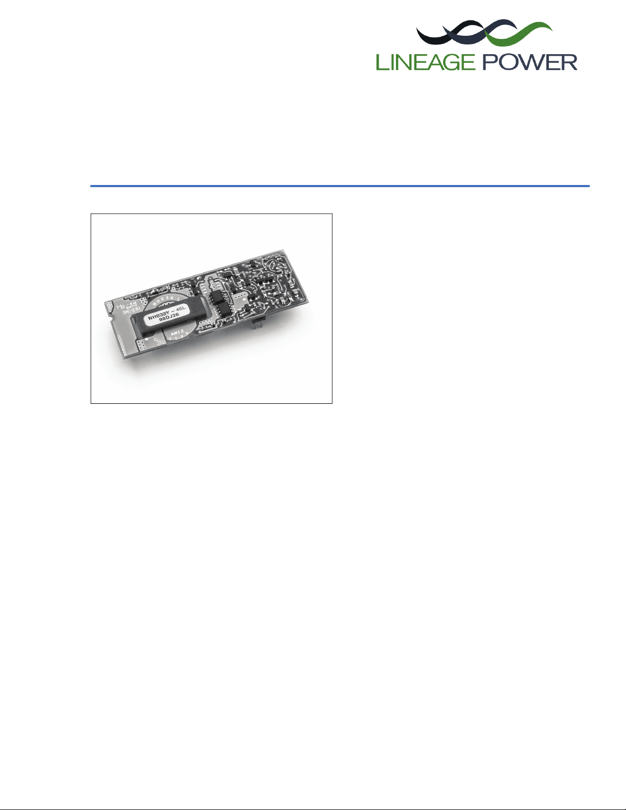
n Small size: 69.9 mm x 25.4 mm x 8.6 mm
(2.75 i
n. x 1.00 in. x 0.34 in.)
n Non-isolated output
n Constant frequency
n High efficiency: 91% typical
The NH033x-L and NH050x-L Series Power Modules use
advanced, surface-mount technology and deliver high-quality, compact, dc-dc conversion at an economical price.
Applications
n Distributed power architectures
n Servers
n Workstations
n Desktop computers
Description
n Overcurrent protection
n Remote on/off
n Output voltage adjustment:
90% to 11
100% t
n Overtemperature protection
n Remote sense
n UL* 60950 Recognized, CSA
0% of V
o 120% of V
00 Certified, VDE 0805 (IEC
n Meets FCC Class A radiated limits
O, nom: VO Š 2.5 V
O, nom: VO < 2.5 V
†
C22.2 No. 60950-
60950) Licensed
Options
n Tight tolerance output
n Short pins: 2.79 mm ± 0.25 mm
(0.11
0 in. ± 0.010 in.)
The NH033x-L and NH050x-L Series Power Modules are non-isolated dc-dc converters that operate over an
input voltag
fra
me power modules have a maximum output current rating of 10 A and 15 A, respectively, at typical full-load
eff
iciencies of 91%.
UL is a registered trademark of Underwriters Laboratories, Inc.
*
† CSA is a registered trademark of Canadian Standards Association.
e range of 4.5 Vdc to 5.5 Vdc and provide a regulated output between 1.2 V and 3.3 V. The open
Page 2
NH033x-L and NH050x-L Series Power Modules: Data Sheet
5 Vdc Input; 1.2 Vdc to 3.3 Vdc Output; 10 A and 15 A March 2010
Absolute Maximum Ratings
Stresses in excess of the absolute maximum ratings can cause permanent damage to the device. These are absolute stress ratings only. Functional operation of the device is not implied at these or any other conditions in excess
of those given in the operations sections of the data sheet. Exposure to absolute maximum ratings for extended
periods can adversely affect device reliability.
Parameter Device Symbol Min Max Unit
Input Voltage (continuous) All V
On/Off Terminal Voltage All V
I —7.0Vdc
on/off —6.0Vdc
Operating Ambient Temperature*:
NH033x-L
NH050x-L
All
All
Storage Temperature All T
* Forced convection—200 lfpm minimum. Higher ambient temperatures possible with increased airflow and/or decreased power output. See the
Thermal Considerations section for more details.
A
T
TA
stg –55 125 °C
0
0
62
49
°C
°C
Electrical Specifications
Unless otherwise indicated, specifications apply over all operating input voltage, resistive load, and temperature
conditions.
Table 1. Input Specifications
Parameter Symbol Min Typ Max Unit
Operating Input Voltage:
Start-up
Continuous Operation
V
VI
I
4.75
4.5
—
5.0
—
5.5
Vdc
Vdc
Maximum Input Current
I = 0 V to 5.5 V; IO = IO, max; see Figures 1—8.):
(V
NH033x-L
NH050x-L
Input Reflected-ripple Current, Peak-to-peak
I, max
I
II, max
I —300—mAp-p
I
—
—
—
—
10
16
A
A
(5 Hz to 20 MHz, 500 nH source impedance;
see Figure 33.)
Input Ripple Rejection (120 Hz) — — 60 — dB
Fusing Considerations
CAUTION: This power module is not internally fused. An input line fuse must always be used.
This power module can be used in a wide variety of applications, ranging from simple stand-alone operation to an
integrated part of a sophisticated power architecture. To preserve maximum flexibility, internal fusing is not
included; however, to achieve maximum safety and system protection, always use an input line fuse. The safety
agencies require a normal-blow fuse with a maximum rating of 20 A (see Safety Considerations section). Based on
the information provided in this data sheet on inrush energy and maximum dc input current, the same type of fuse
with a lower rating can be used. Refer to the fuse manufacturer’s data for further information.
2 Lineage Power
Page 3

Data Sheet NH033x-L and NH050x-L Series Power Modules:
March 2010 5 Vdc Input; 1.2 Vdc to 3.3 Vdc Output; 10 A and 15 A
Electrical Specifications (continued)
Table 2. Output Specifications
Parameter Device Symbol Min Typ Max Unit
Output Voltage Set Point
I = 5.0 V; IO = IO, max; TA = 25 °C)
(V
NH0xxM-L
NH0xxS1R8-L
NH0xxG-L
NH0xxF-L
Output Voltage
(Over all operating input voltage,
resistive load, and temperature
conditions until end of life; see
NH0xxM-L
NH0xxS1R8-L
NH0xxG-L
NH0xxF-L
Figure 35.)
Output Regulation:
Line (V
Load (I
Temperature (T
I = 4.5 V to 5.5 V)
O = 0 to IO, max)
A = 0 °C to 50 °C)
All
All
All
Output Ripple and Noise Voltage
(See Figure 34.):
RMS
Peak-to-peak (5 Hz to 20 MHz)
External Load Capacitance
All
All
All — 0 — 15,000 µF
(See Design Considerations section.)
Output Current
(See Derating Curves Figures 50 and
NH033x-L
NH050x-L
51.)
Output Current-limit Inception
O = 90% of VO, set; TQ32 = 80 °C;
(V
All I
see Feature Descriptions section.)
Output Short-circuit Current All IO —170—%IO, max
Efficiency
I = 5.0 V; IO = IO, max; TA = 25 °C;
(V
see Figure 35.)
NH033M-L
NH033S1R8-L
NH033G-L
NH033F-L
NH050M-L
NH050S1R8-L
NH050G-L
NH050F-L
Switching Frequency All — — 265 — kHz
Dynamic Response
O/Δt = 1 A/10 µs, VI = 5.0 V,
(ΔI
A = 25 °C):
T
Load Change from I
O, max:
I
Peak Deviation
Settling Time (V
O = 0% to 100% of
O < 10% peak
All
All
deviation)
Load Change from I
O, max:
I
Peak Deviation
Settling Time (V
O = 100% to 0% of
O < 10% peak
All
All
deviation)
V
O, set
VO, set
VO, set
VO, set
O
V
VO
VO
VO
—
—
—
—
—
O
I
IO
O 103 — 200 %IO, max
η
η
η
η
η
η
η
η
—
—
—
—
1.45
1.74
2.42
3.18
1.43
1.71
2.40
3.16
—
—
—
—
—
0
0
80
82
87
90
77
81
85
89
—
—
—
—
1.5
1.8
2.5
3.3
—
—
—
—
0.1
0.1
—
—
—
—
—
83
85
89
92
81
83
87
90.5
20
200
20
200
1.55
1.86
2.58
3.39
1.58
1.89
2.60
3.44
0.3
0.3
17
25
100
10.0
15.0
—
—
—
—
—
—
—
—
—
—
—
—
mVrms
mVp-p
Vdc
Vdc
Vdc
Vdc
Vdc
Vdc
Vdc
Vdc
%V
%VO
mV
A
A
%
%
%
%
%
%
%
%
mV
µs
mV
µs
O
Lineage Power 3
Page 4
NH033x-L and NH050x-L Series Power Modules: Data Sheet
5 Vdc Input; 1.2 Vdc to 3.3 Vdc Output; 10 A and 15 A March 2010
General Specifications
Parameter Min Typ Max Unit
Calculated MTBF (I
O = 80% of IO, max; TA = 40 °C) 1,300,000 hours
Weight — — 14 (0.5) g (oz.)
Cleanliness Requirements
The open frame (no case or potting) power modules meet specification J-STD-001B. These requirements state
that any solder balls must be attached and their size should not compromise the minimum electrical spacing of the
power module.
The cleanliness designator of the open frame power module is C00 (per J specification).
Feature Specifications
Unless otherwise indicated, specifications apply over all operating input voltage, resistive load, and temperature
conditions. See Feature Descriptions and Design Considerations sections for further information.
Parameter Symbol Min Typ Max Unit
Remote On/Off Signal Interface
(VI = 4.5 V to 5.5 V; open collector pnp transistor or
equivalent; signal referenced to GND pin; see Figure 38
and Feature Descriptions section.):
Logic Low (ON/OFF pin open)—Module On:
on/off = 0.0 µA
I
on/off = 0.3 V
V
Logic High (V
on/off = 10 mA
I
on/off = 5.5 V
V
Turn-on Time (I
on/off > 2.8 V)—Module Off:
O = IO, max; VO within ±1% of steady
state; see Figures 25—32.)
Output Voltage Adjustment*
(See Feature Descriptions section.):
Output Voltage Remote-sense Range:
O ≥ 2.5 V
For V
O < 2.5 V
For V
Output Voltage Set-point Adjustment Range (Trim):
O ≥ 2.5 V
For V
O < 2.5 V
For V
Overtemperature Protection (shutdown)
(See Feature Descriptions section.)
on/off
V
Ion/off
Von/off
Ion/off
—
—
—
TRIM
V
VTRIM
–0.7
—
—
—
—
—
—
90
100
—
—
—
—
3.0
—
—
—
—
0.3
50
6.0
10
—
10
20
110
120
µA
mA
ms
% V
% VO, nom
% VO, nom
% VO, nom
TQ32 115 120 — °C
V
V
O, nom
Total adjustment of trim and remote sense combined should not exceed 10% for VO ≥ 2.5 V or 20% for VO < 2.5 V.
*
4 Lineage Power
Page 5
Data Sheet NH033x-L and NH050x-L Series Power Modules:
March 2010 5 Vdc Input; 1.2 Vdc to 3.3 Vdc Output; 10 A and 15 A
Characteristics Curves
6
5
(A)
4
3
2
INPUT CURRENT, II
1
0
0.5 1.5 2.5
Figure 1. NH033M-L Input Characteristics,
A = 25 °C
T
10
9
(A)
7
6
5
4
3
INPUT CURRENT, II
2
1
0
0.5
Figure 2. NH050M-L Input Characteristics,
A = 25 °C
T
IO = 10 A
1.0 2.0
INPUT VOLTAGE, V
IO = 15 A
1.0 2.0 3.0 4.0
1.5 2.5
INPUT VOLTAGE, V
3.0
3.5 4.0
I (V)
3.5
I (V)
4.5 5.0
4.5
12
10
(A)
8
6
4
INPUT CURRENT, II
2
0
0.5 1.5 2.5
5.50.0
8-2415
Figure 4. NH050S1R8-L Input Characteristics,
T
9
8
7
(A)
6
5
4
3
INPUT CURRENT, II
2
1
0
5.085.50.0
8-2419
Figure 5. NH033G-L Input Characteristics,
T
IO = 15 A
1.0 2.0
A = 25 °C
0.5
A = 25 °C
3.5 4.0
3.0
INPUT VOLTAGE, V
IO = 10 A
1.51.0 3.5
INPUT VOLTAGE, V
I (V)
I (V)
4.5 5.0
4.0
4.5 5.0
5.50.0
8-2420
5.50.0 2.5 3.02.0
8-2414
(A)
I
INPUT CURRENT, I
14
12
10
8
6
4
2
0
0.5 1.0 3.0 3.5 4.0 4.5
A = 25 °C
T
IO = 15 A
2.0 2.51.5 5.5
INPUT VOLTAGE, V
I
(V)
5.00.0
8-2418
7
(A)
INPUT CURRENT, II
6
5
4
3
2
1
0
0.5 1.0 3.0 3.5 4.0 4.5
IO = 10 A
2.0 2.51.5
INPUT VOLTAGE, V
5.00.0
I (V)
Figure 3. NH033S1R8-L Input Characteristics,
A = 25 °C
T
5.5
8-2416
Figure 6. NH050G-L Input Characteristics,
Lineage Power 5
Page 6
NH033x-L and NH050x-L Series Power Modules: Data Sheet
5 Vdc Input; 1.2 Vdc to 3.3 Vdc Output; 10 A and 15 A March 2010
Characteristics Curves (continued)
9
8
7
(A)
6
5
4
3
INPUT CURRENT, II
2
1
0
Figure 7. NH033F-L Input Characteristics, TA = 25 °C
14
12
(A)
10
8
6
4
INPUT CURRENT, II
2
0
IO = 10 A
1
0.5 1.0 3.0 3.5 4.0 4.5
2 3 5
INPUT VOLTAGE, VI (V)
IO = 15 A
2.0 2.51.5
INPUT VOLTAGE, V
4
I (V)
5.00.0
60
8-2413(C)
5.5
8-2417(C)
1.6
(V)
OUTPUT VOLTAGE, VO
1.4
1.2
1.0
0.8
0.6
0.4
0.2
0.0
8 1012 14 16 2426
6
2
4 20 22
0
OUTPUT CURRENT, I
VI = 5.0 (V)
18
O (A)
8-2427(C)
Figure 10. NH050M-L Current Limit, TA = 25 °C
1.8
1.6
1.4
1.2
1.0
0.8
0.6
0.4
OUTPUT VOLTAGE, V O (V)
0.2
0.0
24 121416
0 810613 57911 13 15 17 20
OUTPUT CURRENT, I
VI = 5.0 V
O
(A)
1819
8-2424(C)
Figure 11. NH033S1R8-L Current Limit, TA = 25 °C
Figure 8. NH050F-L Input Characteristics, TA = 25 °C
1.8
OUTPUT VOLTAGE, V O (V)
1.6
1.4
1.2
1.0
0.8
0.6
0.4
0.2
0.0
0
6
2 4 20 22
8 1012 14 16 2426
OUTPUT CURRENT, I
= 5.0 (V)
VI
18
O (A)
8-2428(C)
Figure 12. NH050S1R8-L Current Limit, TA = 25 °C
OUTPUT VOLTAGE, VO (V)
1.6
1.4
1.2
1.0
0.8
0.6
0.4
0.2
0.0
2 4 12 14 16
0
810613 5 7911131517
OUTPUT CURRENT, I
VI = 5.0 V
(A)
O
18 19
8-2423(C)
Figure 9. NH033M-L Current Limit, TA = 25 °C
6 Lineage Power
Page 7

Data Sheet NH033x-L and NH050x-L Series Power Modules:
March 2010 5 Vdc Input; 1.2 Vdc to 3.3 Vdc Output; 10 A and 15 A
Characteristics Curves (continued)
2.5
2.0
1.5
1.0
0.5
OUTPUT VOLTAGE, VO (V)
0.0
2 4 12 14 16
0
810613 5 7911131517
OUTPUT CURRENT, I
Figure 13. NH033G-L Current Limit, TA = 25 °C
2.5
2.0
(V)
1.5
1.0
0.5
OUTPUT VOLTAGE, VO
0.0
2
0
64 8101214161820
OUTPUT CURRENT, I
VI = 5.0 V
(A)
O
VI = 5.0 V
22 24
O (A)
18 19
26 28
8-2422(C)
8-2426(C)
3.5
(V)
OUTPUT VOLTAGE, V O
3.0
2.5
2.0
1.5
1.0
0.5
0.0
2
0
64 8 1012 14161820
OUTPUT CURRENT, I
VI = 5.0 V
22 24
O (A)
8-2425(C)
Figure 16. NH050F-L Current Limit, TA = 25 °C
86.0
85.5
VI = 4.5 V
85.0
84.5
VI = 5.0 V
84.0
83.5
EFFICIENCY, η (%)
83.0
VI = 5.5 V
82.5
82.0
12 6789
OUTPUT CURRENT, I
O
(A)
100 4 53
8-2431(C)
Figure 17. NH033M-L Efficiency, TA = 25 °C
Figure 14. NH050G-L Current Limit, TA = 25 °C
86
3.5
3.0
VI = 5 V
85
84
VI = 4.5 V
I = 5.0V
V
V
I = 5.5 V
2.5
83
82
EFFICIENCY, η (%)
81
80
1 3 11 13
0 7 95 152 4 6 8 10 12 14
OUTPUT CURRENT, I
O (A)
Figure 18. NH050M-L Efficiency, TA = 25 °C
8-2435(C)
OUTPUT VOLTAGE, VO (V)
2.0
1.5
1.0
0.5
0.0
2 4 12 14 16
0
81061 3 5 7 9 11131517
OUTPUT CURRENT, I
(A)
O
1819
8-2421(C)
Figure 15. NH033F-L Current Limit, TA = 25 °C
Lineage Power 7
Page 8

NH033x-L and NH050x-L Series Power Modules: Data Sheet
5 Vdc Input; 1.2 Vdc to 3.3 Vdc Output; 10 A and 15 A March 2010
Characteristics Curves (continued)
87.5
87.0
86.5
86.0
85.5
85.0
EFFICIENCY, η (%)
84.5
84.0
Figure 19. NH033S1R8-L Efficiency, TA = 25 °C
87.0
86.5
86.0
85.5
85.0
84.5
84.0
EFFICIENCY, η (%)
83.5
83.0
82.5
82.0
VI = 4.5 V
VI = 5.0 V
VI = 5.5 V
12 6789
VI = 4.5 V
VI = 5.0 V
VI = 5.5 V
1 3 11 13
0 7 95 152 4 6 8 10 12 14
4 53
OUTPUT CURRENT, I
OUTPUT CURRENT, I
O (A)
O
(A)
100
8-2432(C)
8-2436(C)
91
VI = 4.5 V
90
VI = 5.0 V
VI = 5.5 V
89
88
87
EFFICIENCY, η (%)
86
85
1 3 11 13
0 7 95 152 4 6 8 10 12 14
OUTPUT CURRENT, I
O (A)
Figure 22. NH050G-L Efficiency, TA = 25 °C
93.0
VI = 4.5 V
92.5
92.0
(%)
EFFICIENCY, η
91.5
91.0
VI = 5.0 V
VI = 5.5 V
90.5
90.5
12 6789
4 53
OUTPUT CURRENT, I
O (A)
Figure 23. NH033F-L Efficiency, TA = 25 °C
8-2434(C)
100
8-2429(C)
Figure 20. NH050S1R8-L Efficiency, TA = 25 °C
93.0
92.5
VI = 4.5 V
I = 5.0 V
V
92.0
V
I = 5.5 V
91.5
91.0
90.5
90.0
EFFICIENCY, η (%)
89.5
89.0
88.5
88.0
1 3 11 13
0 7 95 152 4 6 8 10 12 14
OUTPUT CURRENT, I
O (A)
Figure 24. NH050F-L Efficiency, TA = 25 °C
8-2433(C)
EFFICIENCY, η (%)
90.5
90.0
89.5
89.0
88.5
88.0
87.5
87.0
VI = 4.5 V
VI = 5.0 V
VI = 5.5 V
12 6789
0
4 53 10
OUTPUT CURRENT, I
O
(A)
8-2430(C)
Figure 21. NH033G-L Efficiency, TA = 25 °C
8 Lineage Power
Page 9

Data Sheet NH033x-L and NH050x-L Series Power Modules:
March 2010 5 Vdc Input; 1.2 Vdc to 3.3 Vdc Output; 10 A and 15 A
Characteristics Curves (continued)
V)
ON/OFF (
V
REMOTE ON/OFF,
(1 V/div.)
OUTPUT VOLTAGE, VO (V)
TIME, t (500 µs/div)TIME, t (500 µs/div)
8-2439(C)
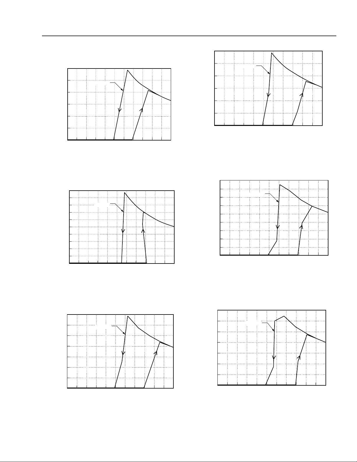
Figure 25. NH033M-L Typical Start-Up from Remote
On/Off, V
I = 5 V, IO = 10 A
ON/OFF (V)
V
REMOTE ON/OFF,
O (V)
(1 V/div.)
OUTPUT VOLTAGE, V
TIME, t (500 µs/div)TIME, t (500 µs/div)
Figure 27. NH033S1R8-L Typical Start-Up from
Remote On/Off, V
(V)
I = 5 V, IO = 10 A
8-2440(C)
(V)
ON/OFF
V
REMOTE ON/OFF,
(V)
O
(500 mV/div.)
OUTPUT VOLTAGE, V
TIME, t (500 µs/div)TIME, t (500 µs/div)
8-2442(C)
Figure 26. NH050M-L Typical Start-Up from Remote
On/Off, V
I = 5 V, IO = 15 A
ON/OFF
V
REMOTE ON/OFF,
(V)
O
(1 V/div.)
OUTPUT VOLTAGE, V
TIME, t (500 µs/div)TIME, t (500 µs/div)
Figure 28. NH050S1R8-L Typical Start-Up from
Remote On/Off, V
I = 5 V, IO = 15 A
8-2452(C)
Lineage Power 9
Page 10

NH033x-L and NH050x-L Series Power Modules: Data Sheet
5 Vdc Input; 1.2 Vdc to 3.3 Vdc Output; 10 A and 15 A March 2010
Characteristics Curves (continued)
V)
VON/OFF (
REMOTE ON/OFF,
(1 V/div.)
OUTPUT VOLTAGE, VO (V)
TIME, t (500 µs/div)TIME, t (500 µs/div)
8-2438(C)
Figure 29. NH033G-L Typical Start-Up from Remote
On/Off, V
I = 5 V, IO = 10 A
ON/OFF (V)
V
REMOTE ON/OFF,
O (V)
(1 V/div.)
OUTPUT VOLTAGE, V
TIME, t (500 µs/div)
8-2437(C)
Figure 31. NH033F-L Typical Start-Up from Remote
On/Off, V
V)
I = 5 V, IO = 10 A
ON/OFF (V)
V
REMOTE ON/OFF,
(1 V/div.)
OUTPUT VOLTAGE, VO (V)
TIME, t (500 µs/div)TIME, t (500 µs/div)
8-2443(C)
Figure 30. NH050G-L Typical Start-Up from Remote
On/Off, V
I = 5 V, IO = 15 A
VON/OFF (
REMOTE ON/OFF,
(1 V/div.)
OUTPUT VOLTAGE, VO (V)
TIME, t (500 µs/div)TIME, t (500 µs/div)
8-2441(C)
Figure 32. NH050F-L Typical Start-Up from Remote
On/Off, V
I = 5 V, IO = 15 A
1010 Lineage Power
Page 11

Data Sheet NH033x-L and NH050x-L Series Power Modules:
March 2010 5 Vdc Input; 1.2 Vdc to 3.3 Vdc Output; 10 A and 15 A
Test Configurations
Note: Input reflected-ripple current is measured with a simulated
Note: Use a 0.1 µF ceramic capacitor and a 1,000 µF aluminum or
TO OSCILLOSCOPE
CURRENT
L
TEST
500 µH
S
220 µF
C
BATTERY
ESR < 0.1 Ω
@ 20 ˚C, 100 kHz
source impedance of 500 nH. Capacitor C
PROBE
CI 470 µF
ESR < 0.2 Ω
@ 100 kHz
S offsets possible
battery impedance. Current is measured at the input of the
module.
Figure 33. Input Reflected-Ripple Test Setup
COPPER STRIP
VO
1.0 µF
GND
1000 µF
SCOPE
tantalum capacitor (ESR = 0.05 ¾ @ 100 kHz). Scope measurement should be made using a BNC socket. Position the
load between 50 mm and 80 mm (2 in. and 3 in.) from the
module.
RESISTIVE
LOAD
I
(+)
V
GND
8-203(C).h
8-513(C).r
Design Considerations
Input Source Impedance
The power module should be connected to a low acimpedance input source. Highly inductive source
impedances can affect the stability of the NH033x-L
and NH050x-L Series Power Modules. Adding external
capacitance close to the input pins of the module can
reduce the ac impedance and ensure system stability.
The minimum recommended input capacitance (C
a 470 µF electrolytic capacitor with an ESR ð 0.02 Ω @
100 kHz. Verify the quality and layout of these capacitors by ensuring that the ripple across the module input
pins is less than 1 Vp-p at I
O = IO, max. (See Figures 33,
36, and 37.)
The 470 µF electrolytic capacitor (C
1) should be added
across the input of the NH033x-L or NH050x-L to
ensure stability of the unit. The electrolytic capacitor
should be selected for ESR and RMS current ratings to
ensure safe operation in the case of a fault condition.
The input capacitor for the NH033x-L and NH050x-L
series should be rated to handle 10 Arms.
When using a tantalum input capacitor, take care not to
exceed the tantalum capacitor power rating because of
the capacitor’s failure mechanism (for example, a short
circuit).
TO OSCILLOSCOPE
CURRENT
SOURCE
PROBE
L
1 µH (MAX)
1) is
V
I
Figure 34. Peak-to-Peak Output Noise
Measurement Test Setup
CONTACT AND
DISTRIBUTION LOSSES
IO
SUPPLY
V I VO
II
GND
SENSE(+)
SENSE(-)
LOAD
SUPPLY
Figure 36. Setup with External Capacitor to Reduce
Input Ripple Voltage
C
1
470 µF
+
2
C
10 µF (MAX)
GND
8-1215(C).a
To reduce the amount of ripple current fed back to the
CONTACT RESISTANCE
8-1173(C).a
Note: All measurements are taken at the module terminals. When
socketing, place Kelvin connections at module terminals to
avoid measurement errors due to socket contact resistance.
O IO×
V
η
------------------------
VI II×
x100= %
input supply (input reflected-ripple current), an external
input filter can be added. Up to 10 µF of ceramic
capacitance (C
2) may be externally connected to the
input of the NH033x-L or NH050x-L, provided the
source inductance (L
SOURCE) is less than 1 µH (see
Figure 36).
Figure 35. Output Voltage and Efficiency
Measurement Test Setup
Lineage Power 11
Page 12

NH033x-L and NH050x-L Series Power Modules: Data Sheet
5 Vdc Input; 1.2 Vdc to 3.3 Vdc Output; 10 A and 15 A March 2010
Design Considerations (continued)
Input Source Impedance (continued)
To further reduce the input reflected ripple current, a
filter inductor (L
supply and the external input capacitors (see Figure
37). The filter inductor should be rated to handle the
maximum power module input current of 10 Adc for the
NH033x-L and 16 Adc for the NH050x-L.
If the amount of input reflected-ripple current is unacceptable with an external L-C filter, more capacitance
may be added across the input supply to form a C-L-C
filter. For best results, the filter components should be
mounted close to the power module.
TO OSCILLOSCOPE
Figure 37. Setup with External Input Filter to
FILTER) can be connected between the
CURRENT
PROBE
L
SOURCE
SUPPLY
L
FILTER
+
C
470 µF
1
C
2
Reduce Input Reflected-Ripple Current
and Ensure Stability
V
I
GND
8-1216(C).a
Safety Considerations
For safety-agency approval of the system in which the
power module is used, the power module must be
installed in compliance with the spacing and separation
requirements of the end-use safety agency standard,
i.e., UL 60950, CSA C22.2 No. 60950-00, and VDE
0805 (IEC60950).
For the converter output to be considered meeting the
requirements of safety extra-low voltage (SELV), the
input must meet SELV requirements.
The power module has extra-low voltage (ELV) outputs
when all inputs are ELV.
The input to these units is to be provided with a maximum 20 A normal-blow fuse in the ungrounded lead.
Feature Descriptions
Overcurrent Protection
To provide protection in a fault condition, the unit is
equipped with internal overcurrent protection. The unit
operates normally once the fault condition is removed.
Under some extreme overcurrent conditions, the unit
may latch off. Once the fault is removed, the unit can
be reset by toggling the remote on/off signal for one
second or by cycling the input power.
Output Capacitance
The NH033x-L and NH050x-L Series Power Modules
can be operated with large values of output capacitance. In order to maintain stability, choose a capacitor
bank so that the product of their capacitance and ESR
is greater than 50 x 10
50 x 10
–6
). For complex or very low ESR filters, consult
the Technical Support for stability analysis.
–6
(e.g., 1,000 µF x 0.05 Ω =
Remote On/Off
To turn the power module on and off, the user must
supply a switch to control the voltage at the ON/OFF
on/off). The switch should be an open collector pnp
pin (V
transistor connected between the ON/OFF pin and the
I pin or its equivalent (see Figure 38).
V
During a logic low when the ON/OFF pin is open, the
power module is on and the maximum V
on/off generated
by the power module is 0.3 V. The maximum allowable
leakage current of the switch when V
I = 5.5 V (Vswitch = 5.2 V) is 50 µA.
V
During a logic high, when V
on/off = 2.8 V to 5.5 V, the
power module is off and the maximum I
on/off = 0.3 V and
on/off is 10 mA.
The switch should maintain a logic high while sourcing
10 mA.
Leave the remote ON/OFF pin open if not using that
feature.
The module has internal capacitance to reduce noise
at the ON/OFF pin. Additional capacitance is not generally needed and may degrade the start-up characteristics of the module.
1212 Lineage Power
Page 13

Data Sheet NH033x-L and NH050x-L Series Power Modules:
March 2010 5 Vdc Input; 1.2 Vdc to 3.3 Vdc Output; 10 A and 15 A
Feature Descriptions (continued)
Remote On/Off (continued)
CAUTION: Never ground the ON/OFF pin. Ground-
ing the ON/OFF pin disables an important safety feature and may damage the
module or the customer system.
V
I
ON/OFF
GND
switch
V
V
on/off
+
I
on/off
+
Figure 38. Remote On/Off Implementation
Remote Sense
Remote sense minimizes the effects of distribution
losses by regulating the voltage at the remote-sense
connections. The voltage between the remote-sense
pins and the output pins must not exceed the output
voltage sense range given in the Feature Specifications
table.
The voltage between the V
exceed 110% of V
O, nom for VO < 2.5 V. This limit includes any increase
V
O, nom for VO ≥ 2.5 V or 120% of
in voltage due to remote-sense compensation and output voltage set-point adjustment (trim), see Figure 39.
O and GND pins must not
Vo
8-1175(C).a
Output Voltage Set-Point Adjustment (Trim)
Output voltage set-point adjustment allows the output
voltage set point to be increased or decreased by connecting an external resistor between the TRIM pin and
either the SENSE(+) pin (decrease output voltage) or
SENSE(–) pin (increase output voltage). The trim
range for modules that produce 2.5 V
±10% of V
duce less than 2.5 V
O, nom. The trim range for modules that pro-
O is +20%, –0%.
Connecting an external resistor (R
TRIM and SENSE(+) pin decreases the output voltage
set point as defined in the following equation.
For the F (3.3 V
Rtrim-down
For the G (2.5 V
R
trim-down
O) module:
18.23
⎛⎞
------------------------------47.2–
⎝⎠
O VO adj,–
V
O) module:
6.98
⎛⎞
------------------------------24–
⎝⎠
O VO adj,–
V
Note: Output voltages below 2.5 V cannot be trimmed
down.
Connecting an external resistor (R
TRIM and SENSE(–) pins increases the output voltage
set point to V
For the G (2.5 V
R
trim-up
O, adj as defined in the following equation.
O) module:
28
⎛⎞
------------------------------10–
⎝⎠
O adj, VO–
V
For all other modules:
28
R
trim-up
⎛⎞
------------------------------33.2–
⎝⎠
O adj, VO–
V
Leave the TRIM pin open if not using that feature.
O or greater is
trim-down) between the
kΩ=
kΩ=
trim-up) between the
kΩ=
kΩ=
If not using the remote-sense feature to regulate the output at the point of load, connect SENSE(+) to V
O and
Overvoltage Protection
SENSE(–) to GND at the module.
Overvoltage protection is not provided in the power
SENSE(+)
SENSE(-)
V
II
CONTACT
RESISTANCE
SUPPLY LOAD
VO
I
GND
IO
CONTACT AND
DISTRIBUTION LOSSES
8-651(C).i
module. External circuitry is required to provide overvoltage protection.
Figure 39. Effective Circuit Configuration for
Single-Module Remote-Sense Operation
Lineage Power 13
Page 14

NH033x-L and NH050x-L Series Power Modules: Data Sheet
5 Vdc Input; 1.2 Vdc to 3.3 Vdc Output; 10 A and 15 A March 2010
Feature Descriptions (continued)
Overtemperature Protection
To provide additional protection in a fault condition, the
unit is equipped with a nonlatched thermal shutdown
circuit. The shutdown circuit engages when Q32
exceeds approximately 120 °C. The unit attempts to
restart when Q32 cools down. The unit cycles on and
off if the fault condition continues to exist. Recovery
from shutdown is accomplished when the cause of the
overheating condition is removed.
Thermal Considerations
The power modules operate in a variety of thermal
environments; however, sufficient cooling should be
provided to help ensure reliable operation of the unit.
Heat is removed by conduction, convection, and radiation to the surrounding environment.
The thermal data presented is based on measurements taken in a wind tunnel. The test setup shown in
Figure 40 was used to collect data for Figures 50 and
51. Note that the airflow is parallel to the long axis of
the module. The derating data applies to airflow along
either direction of the module’s long axis.
The module runs cooler when it is rotated 90° from the
direction shown in Figure 40. This thermally preferred
orientation increases the maximum ambient temperatures 4 °C to 5 °C from the maximum values shown in
Figures 50 and 51.
Proper cooling can be verified by measuring the power
module’s temperature at lead 7 of Q32 as shown in
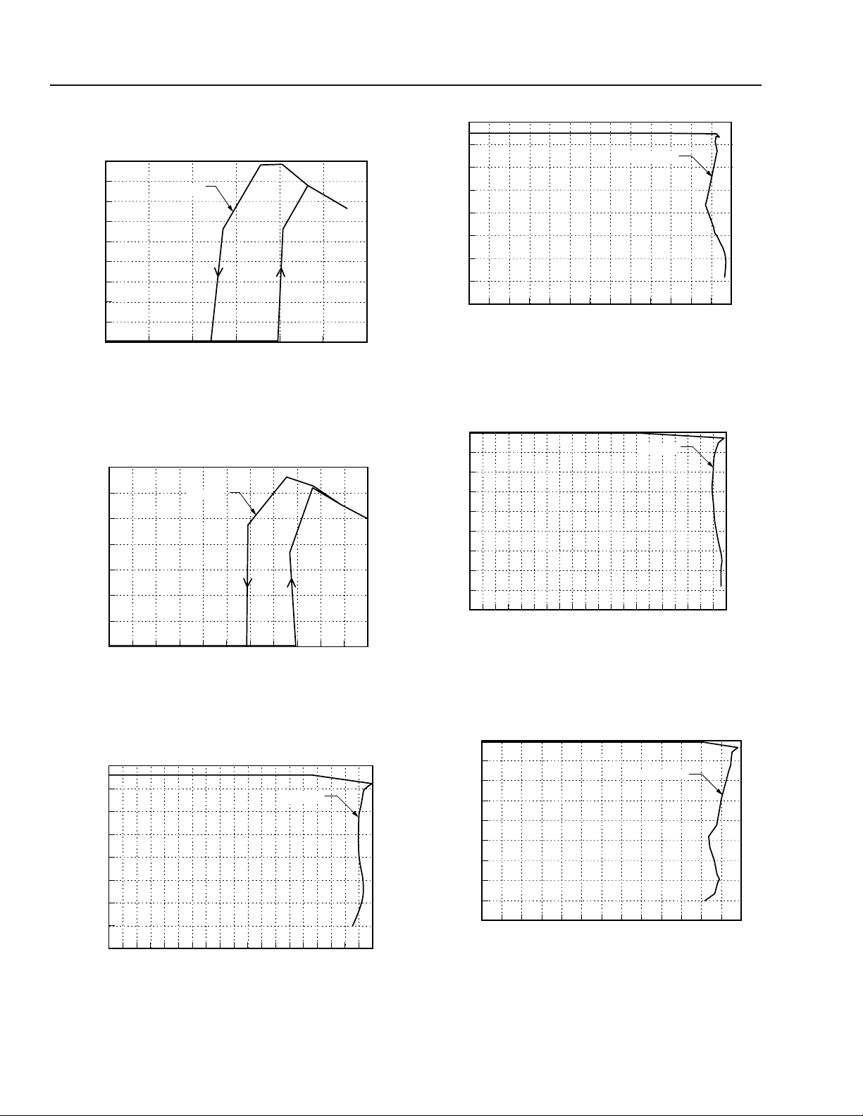
Figure 41.
Q32
LEAD #7
8-1149(C).b
Figure 41. Temperature Measurement Location
The temperature at this location should not exceed
115 °C at full power. The output power of the module
should not exceed the rated power.
Convection Requirements for Cooling
To predict the approximate cooling needed for the module, determine the power dissipated as heat by the unit
for the particular application. Figures 42 through 49
show typical power dissipation for the module over a
range of output currents.
3.5
3.0
(W)
203.2 (8.0)
25.4 (1.0)
POWER MODULE
AIRFLOW
AIR VELOCITY
AND AMBIENT
TEMPERATURE
MEASURED HERE
2.5
2.0
1.5
1.0
POWER DISSIPATION, PD
0.5
12 6789
VI = 5.5 V
VI = 5.0 V
VI = 4.5 V
4 53
OUTPUT CURRENT, I
100
O (A)
8-2446(C)
Figure 42. NH033M-L Typical Power Dissipation vs.
A = 25 °C
Note: Dimensions are in millimeters and (inches).
76.2 (3.0)
Output Current, T
8-1199(C).a
Figure 40. Thermal Test Setup
1414 Lineage Power
Page 15

Data Sheet NH033x-L and NH050x-L Series Power Modules:
March 2010 5 Vdc Input; 1.2 Vdc to 3.3 Vdc Output; 10 A and 15 A
Thermal Considerations (continued)
Convection Requirements for Cooling
(continued)
6.0
5.5
5.0
(W)
4.5
4.0
3.5
3.0
2.5
2.0
1.5
POWER DISSIPATION, PD
1.0
0.5
1 3 11 13
0 7 95 152 4 6 8 10 12 14
Figure 43. NH050M-L Typical Power Dissipation vs.
Output Current, T
3.5
VI = 5.5 V
VI = 5.0 V
VI = 4.5 V
OUTPUT CURRENT, I
A = 25 °C
O (A)
8-2450(C)
6.0
5.5
5.0
(W)
D
4.5
4.0
3.5
3.0
2.5
2.0
1.5
POWER DISSIPATION, P
1.0
0.5
1 3 11 13
0 7 95 152 4 6 8 10 12 14
VI = 5.5 V
VI = 5.0 V
VI = 4.5 V
OUTPUT CURRENT, I
O
(A)
8-2451(C)
Figure 45. NH050S1R8-L Typical Power Dissipation
A = 25 °C
(W)
vs. Output Current, T
3.5
3.0
2.5
2.0
VI = 5.5 V
VI = 5.0 V
VI = 4.5 V
3.0
(W)
2.5
2.0
1.5
1.0
POWER DISSIPATION, PD
0.5
12 6789
VI = 5.5 V
VI = 5.0 V
VI = 4.5 V
4 53
OUTPUT CURRENT, I
100
O (A)
8-2447(C)
Figure 44. NH033S1R8-L Typical Power Dissipation
vs. Output Current, T
A = 25 °C
1.5
1.0
POWER DISSIPATION, P D
0.5
12 6789
4 53
OUTPUT CURRENT, I
O (A)
8-2445(C)
100
Figure 46. NH033G-L Typical Power Dissipation vs.
Output Current, T
A = 25 °C
Lineage Power 15
Page 16

NH033x-L and NH050x-L Series Power Modules: Data Sheet
5 Vdc Input; 1.2 Vdc to 3.3 Vdc Output; 10 A and 15 A March 2010
Thermal Considerations (continued)
Convection Requirements for Cooling
(continued)
6.0
5.5
5.0
(W)
D
4.5
4.0
3.5
3.0
2.5
2.0
1.5
POWER DISSIPATION, P
1.0
0.5
1 3 11 13
0 7 95 152 4 6 8 10 12 14
Figure 47. NH050G-L Typical Power Dissipation vs.
3.5
3.0
(W)
2.5
2.0
1.5
1.0
POWER DISSIPATION, PD
0.5
VI = 5.5 V
VI = 5.0 V
VI = 4.5 V
O
OUTPUT CURRENT, I
Output Current, T
VI = 5.5 V
VI = 5.0 V
VI = 4.5 V
12 6789
A = 25 °C
4 53
(A)
8-2449(C)
100
6.0
5.5
5.0
(W)
D
4.5
4.0
3.5
3.0
2.5
2.0
1.5
POWER DISSIPATION, P
1.0
0.5
1 3 11 13
0 7 95 152 4 6 8 10 12 14
VI = 5.5 V
VI = 5.0 V
VI = 4.5 V
OUTPUT CURRENT, I
O
(A)
8-2448(C)
Figure 49. NH050F-L Typical Power Dissipation vs.
Output Current, T
A = 25 °C
With the known power dissipation and a given local
ambient temperature, the minimum airflow can be chosen from the derating curves in Figures 50 and 51.
4
TYPICAL 5.5 VI,
OUT DISSIPATION
10 A
3
2
1
POWER DISSIPATION, PD (W)
0
0 25 45 55 125
NATURAL
CONVECTION
0.5 m/s (100 ft./min.)
1.0 m/s (200 ft./min.)
1.5 m/s (300 ft./min.)
2.0 m/s (400 ft./min.)
3.0 m/s (600 ft./min.)
35 65
AMBIENT TEMPERATURE, T
TYPICAL 5.0 VI,
10 A
OUT DISSIPATION
75 85 95 105
A (˚C)
115
8-1425(C).c
OUTPUT CURRENT, I
O (A)
8-2444(C)
Figure 50. NH033x-L Power Derating vs. Local
Ambient Temperature and Air Velocity
Figure 48. NH033F-L Typical Power Dissipation vs.
Output Current, T
A = 25 °C
1616 Lineage Power
Page 17

Data Sheet NH033x-L and NH050x-L Series Power Modules:
March 2010 5 Vdc Input; 1.2 Vdc to 3.3 Vdc Output; 10 A and 15 A
Thermal Considerations (continued)
Convection Requirements for Cooling
(continued)
6
5
4
NATURAL
CONVECTION
3
0.5 m/s (100 ft./min.)
1.0 m/s (200 ft./min.)
1.5 m/s (300 ft./min.)
2
2.0 m/s (400 ft./min.)
POWER DISSIPATION, PD (W)
3.0 m/s (600 ft./min.)
1
0
5 15 35 45 115
25 55
AMBIENT TEMPERATURE, T
65 75 85 95 105
TYPICAL 5.5 VI,
15 AOUT DISSIPATION
TYPICAL 5.0 VI,
15 AOUT
DISSIPATION
A (˚C)
For example, if the NH050F-L dissipates 4 W of heat,
the minimum airflow in a 65 °C environment is 1 m/s
(200 ft./min.).
Keep in mind that these derating curves are approximations of the ambient temperatures and airflows
required to keep the power module temperature below
its maximum rating. Once the module is assembled in
the actual system, the module’s temperature should be
checked as shown in Figure 41 to ensure it does not
exceed 115 °C.
8-1426(C).b
Figure 51. NH050x-L Power Derating vs. Local
Ambient Temperature and Air Velocity
Lineage Power 17
Page 18

NH033x-L and NH050x-L Series Power Modules: Data Sheet
0
5 Vdc Input; 1.2 Vdc to 3.3 Vdc Output; 10 A and 15 A March 2010
Outline Diagram
Dimensions are in millimeters and (inches).
Tolerances: x.x mm ± 0.5 mm (x.xx in. ± 0.02 in.), x.xx mm ± 0.25 mm (x.xxx in. ± 0.010 in.).
Top View
Side View
25.4
(1.00)
SQUARE PIN
0.64 x 0.64
(0.025 x 0.025)
69.9 (2.75)
5.84
(0.230)
LABEL*
25.4
(1.00)
8.6
(0.34)
MAX
Bottom View
48.3 (1.90)
45.7 (1.80)
43.2 (1.70)
40.6 (1.60)
2.54 (0.100)
* Label includes product designation and date code.
17.3
(0.68)
1.8
(0.07)
(0.100)
2.54
5.08
(0.200)
(0.300)
7.62
17.8
(0.70)
20.3
(0.8
8-1176(C).b
18 Lineage Power
Page 19

Data Sheet NH033x-L and NH050x-L Series Power Modules:
2
0
March 2010 5 Vdc Input; 1.2 Vdc to 3.3 Vdc Output; 10 A and 15 A
Recommended Hole Pattern
Dimensions are in millimeters and (inches).
Tolerances: x.xx mm ± 0.13 mm (x.xxx in. ± 0.005 in.).
PLATED HOLE SIZE
1.32 (0.052)
25.9
(1.02)
MAX
70.4 (2.77) MAX
J2
14
58
40.64 (1.600)
43.18 (1.700)
45.72 (1.800)
48.26 (1.900)
2.54 (0.100)
54
81
J1
2.54
(0.100)
2.03
(0.080)
17.53
(0.690)
7.62
(0.300)
(0.700)
5.08
(0.200)
PinFunctionPinFunction
J1 - 1 Remote On/Off J2 - 1 SENSE (–)
J1 - 2 No Connection J2 - 2 SENSE (+)
J1 - 3 TRIM J2 - 3 V
O
J1 - 4 GND J2 - 4 VO
J1 - 5 GND J2 - 5 VO
J1 - 6 VI J2 - 6 VO
J1 - 7 VI J2 - 7 GND
J1 - 8 V
I J2 - 8 GND
17.78
20.3
(0.80
8-1176(C).b
Lineage Power 19
Page 20

NH033x-L and NH050x-L Series Power Modules: Data Sheet
Wor ld Wide Headqu arters
L ine age P ower C orp ora tion
601 Shiloh Road, Plano, TX 75074, USA
+1-800-526-7 819
(Outside U.S.A.: +1-97 2-244 -9428)
www .linea gepo wer .com
e-ma il: tec hs uppor t1@ lin ea gep ower .c om
A s ia -P a cific Hea dquarter s
Tel: +65 6593 7211
E urope, M iddle-E a s t an d Afr ica Headquarter s
Tel: +49 898 780 672 80
Indi a H eadquarte rs
Tel: +91 80 28411633
Lineage Power reserves the right to make changes to the product(s) or information contained herein without notice. No liability is assumed as a res ult of their use or
application. No rights under any pate nt accompany the sale of any such product(s) or information.
Lineage Power DC-DC products are protected under various patents. Information on these patents is available at www.lineagepower.com/patents.
© 2009 Lineage Power Corporation, (Plano, Texas) All Inte rnational Rights Reserved.
5 Vdc Input; 1.2 Vdc to 3.3 Vdc Output; 10 A and 15 March 2010
Ordering Information
Please contact your Lineage Power Account Manager or Field Application Engineer for pricing and availability.
Ta
ble 3. Device Codes
Input Vo
ltage Output Voltage Output Power Device Code Comcode
5 V 1
5 V 1.
5 V 2.5 V 25 W N
5 V 3
5 V 1
5 V 1.
5 V 2
5 V 3
le 4. Device Options
Tab
Tight to
Sho
rt pins: 2.79 mm ± 0.25 mm
0 in. ± 0.010 in.)
(0.11
.5 V 15 W NH033M-L 107993685
8 V 18 W NH033S1R8-L 107940306
.3 V 33 W NH033F-L 107859928
.5 V 22.5 W NH050M-L 107993693
8 V 27 W NH050S1R8-L 107940314
.5 V 37.5 W NH050G-L 107917130
.3 V 50 W NH050F-L 107917148
Option S
uffix
lerance output 2
H033G-L 107917122
8
April 2008
FDS01-070EPS (Replaces FDS01-069EPS)
 Loading...