

Page 1
Data Sheet
October 14, 2009
RoHS Compliant
Applications
n
Distributed Power Architectures
n
Communication Equipment
n
Computer Equipment
NH020-Series Power SIPs:
5 Vdc Input; 1.5 Vdc to 3.3 Vdc Output; 20 W
Features
n
Compatible with RoHS EU Directive 200295/EC
n
Compatible in Pb- free or SnPb reflow environment
n
Nonisolated output
n
High efficiency: 86% typical
n
Small size and low profile:
63.5 mm x 5.6 mm x 14 mm
(2.5 in x 0.22 in x 0.55 in)
n
Remote On/Off
n
Output overcurrent protection
n
Output voltage adjustment
n
Overtemperature protection
n
UL* 60950 Recognized, CSA† C22.2 No. 60950-00 Certi-
fied, and VDE‡ 0805 (IEC60950, 3rd edition) Licensed
n
Meets FCC classA radiated limits
Options
n
Tight Tolerance output
n
-40 °C operation
Description
The NH020-Series Power SIPs are nonisolated dc-dc converters that operate over an input voltage range of 4.5 Vdc to 5.5
Vdc and provide a precisely regulated dc output. The SIPs have a maximum output current rating of 6 A at a typical full-load
efficiency of 86%. Standard features include remote on/off and output voltage adjustment
* UL is a registered trademark of Underwriters Laboratories, Inc.
† CSA is a registered trademark of Canadian Standards Association.
PDF Name:DS00-128E
.
Document Name:
PS (Replaces DS00-127EPS)
Page 2

Data Sheet
October 14, 2009
5 Vdc Input; 1.5 Vdc to 3.3 Vdc Output; 20 W
NH020-Series Power SIPs:
Absolute Maximum Ratings
Stresses in excess of the absolute maximum ratings can cause permanent damage to the device. These are absolute stress
ratings only, functional operation of the device is not implied at these or any other conditions in excess of those given in the
operations sections of the data sheet. Exposure to absolute maximum ratings for extended periods can adversely affect the
device reliabiltiy.
Parameter Symbol Min Max Unit
Input Voltage:
Continuous VIN 0 7.0 Vdc
Operating Ambient Temperature* T
Storage Temperature Tstg –55 125 °C
On/Off Terminal Voltage Von/off — 6.0 Vdc
* Forced convection—1.5 ms–1 (300 lfm) minimum. Higher ambient temperatures are possible with increased airflow and/or decreased power
output. See the Thermal Considerations section for more details.
† The –40 °C operation is optional. See Ordering Information section.
Q31
–40/0
†
115 °C
Electrical Specifications
Unless otherwise indicated, specifications apply over all operating input voltage, resistive load, and temperature conditions.
Parameter Symbol Min Typ Max Unit
Operating Input Voltage VI 4.5 5.0 5.5 Vdc
Maximum Input Current
(VI = 0 to VI,max; IO = IO,max)
Inrush Transient i
Input Reflected-Ripple Current
(5 Hz to 20 MHz; 500nH source impedance;See Figure 14)
Input Ripple Rejection
(100 - 120Hz)
II,max — 6.1 A
2
t——1A
625 mAp-p
60 dB
2
s
CAUTION: This power module is not internally fused. An input line fuse must always be used.
This power SIP can be used in a wide variety of applications, ranging from simple stand-alone operation to an
integrated part of a sophisticated power architecture. To preserve maximum flexibility, internal fusing is not included; however,
to achieve maximum safety and system protection, always use an input line fuse. The safety agencies require a normal-blow
fuse with a maximum rating of 10 A (see Safety Considerations section). To aid in the proper fuse selection for the given application, information on inrush energy and maximum dc input current is provided. Refer to the fuse manufacturer’s data for further information.
Lineage Power 2
Page 3

Data Sheet
October 14, 2009
5 Vdc Input; 1.5 Vdc to 3.3 Vdc Output; 20 W
NH020-Series Power SIPs:
Electrical Specifications (continued)
Parameter Device Symbol Min Typ Max Unit
Output Voltage Set Point
(VI = 5.0 V; IO = IO, max; TA = 25 °C)
Output Voltage
(Over all operating input voltage, resistive load, and
temperature conditions until end of life.)
Output Regulation:
Line (VI = 4.5 V to 5.5 V)
Load (IO = 0 to IO, max)
Temperature (TA = 0 °C to 55 °C)
Ripple and Noise Voltage
Output
(See Figures 7—9 and 15.):
RMS
Peak-to-peak (5 Hz to 20 MHz)
External Load Capacitance (electrolytic) All — 0 — 10,000 µF
Output Current
(Forced convection, 1.5 ms
Output Current-limit Inception
(VO = 90% of VO, set; see Feature Descriptions
section.)
Efficiency
(VI = 5.0 V; IO = IO, max; TA = 25 °C; see Figures 3—6
and 16.)
Switching Frequency All — — 500 — kHz
Dynamic Response
(ΔIO/Δt = 1 A/10 µs, VI = 5.0 V, TA = 25 °C;
see Figures 10 and 11.):
Load Change from IO = 0% to 100% of IO, max:
Peak Deviation
Settling Time (VO < 10% peak deviation)
Load Change from IO = 100% to 0% of IO, max:
Peak Deviation
Settling Time (VO < 10% peak deviation)
–1
(300 lfm))
NH020M
NH020M2
NH020Y
NH020Y2
NH020G
NH020F
NH020F2
NH020M
NH020M2
NH020Y
NH020Y2
NH020G
NH020F
NH020F2
All
M
Y
F, G
All
F, G, M
Y
All
All IO 0 — 6 A
All IO — 350 — %IO, max
NH020M
NH020Y
NH020G
NH020F
All
All
All
All
VO, set
VO, set
VO, set
VO, set
VO, set
VO, set
VO, set
VO
VO
VO
VO
VO
VO
VO
—
—
—
—
—
—
—
—
h
h
h
h
—
—
—
—
1.46
1.485
1.75
1.782
2.43
3.18
3.27
1.43
1.455
1.716
1.745
2.39
3.16
3.24
—
—
—
—
—
—
—
—
70
73
79
84
—
—
—
—
1.5
1.5
1.8
1.8
2.5
3.3
3.3
—
—
—
—
—
—
—
0.1
0.4
0.3
0.1
—
—
—
—
72
75
82
86
80
200
80
200
1.54
1.515
1.85
1.818
2.57
3.39
3.33
1.57
1.545
1.883
1.855
2.61
3.44
3.36
0.4
0.6
0.5
0.3
17
25
30
100
—
—
—
—
—
—
—
—
%VO
%VO
%VO
%VO
mVrms
mVrms
mVp-p
Vdc
Vdc
Vdc
Vdc
Vdc
Vdc
Vdc
Vdc
Vdc
Vdc
Vdc
Vdc
Vdc
Vdc
mV
%
%
%
%
mV
µs
mV
µs
General Specifications
Parameter Min Typ Max Unit
Calculated MTBF (IO = 80% of IO, max TA = 25 °C) 1,400,000 Hours
Weight — — 7(0.25) g (oz.)
Lineage Power 3
Page 4

Data Sheet
October 14, 2009
5 Vdc Input; 1.5 Vdc to 3.3 Vdc Output; 20 W
NH020-Series Power SIPs:
Feature Specifications
Unless otherwise indicated, specifications apply over all operating input voltage, resistive load, and temperature conditions.
See Feature Descriptions for additional information
Parameter Device Symbol Min Typ Max Unit
Remote On/Off Signal Interface
(VI = VI,min to VI, max; open collector pnp or Compatible, Von/off
signal referenced to GND. See Figure 20 and Feature
Descriptions section)
Logic Low (ON/OFF pin open—Module On)
Ion/off = 0.0 µA
Von/off = 0.3 V
Logic High (VON/OFF > 2.8 V)—Module Off
Ion/off = 10 mA
Von/off = 5.5 V
Turn-on Time
(IO = 80% of IO, max; VO within ±1% of steady state; see
Figure 12)
Output Voltage Set-point Adjustment Range NH020M
Overtemperature Protection (shutdown) All TQ31 — 125 — °C
.
All
All
All
All
All
NH020Y
NH020G
NH020F
Von/off
Ion/off
Von/off
Ion/off
—
Vtrim
Vtrim
Vtrim
Vtrim
–0.7
100
100
90
84
1.5
—
—
—
—
0.3
50
6.0
10
5.0
150
120
110
110
V
µA
V
mA
ms
%VO,
nom
%VO,
nom
Lineage Power 4
Page 5
Data Sheet
October 14, 2009
5 Vdc Input; 1.5 Vdc to 3.3 Vdc Output; 20 W
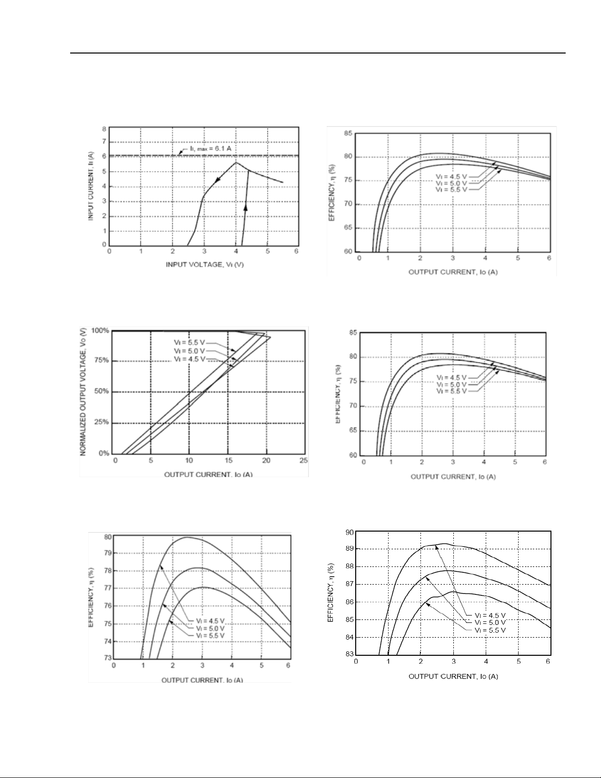
Characteristic Curves
The following figures provide typical characteristics curves (TA = 25 °C).
NH020-Series Power SIPs:
Figure 1. Typical Inpu t Characteristics at 6 A output
current.
Figure 2. Typical Output Chara cteristics.
Figure 4. Typical Efficiency for NH020Y.
Figure 5. Typical Efficiency for NH020A0G.
Figure 3. T ypical Efficiency for NH020M .
Lineage Power 5
Figure 6. Typical Efficiency for NH020F.
Page 6
Data Sheet
October 14, 2009
5 Vdc Input; 1.5 Vdc to 3.3 Vdc Output; 20 W
NH020-Series Power SIPs:
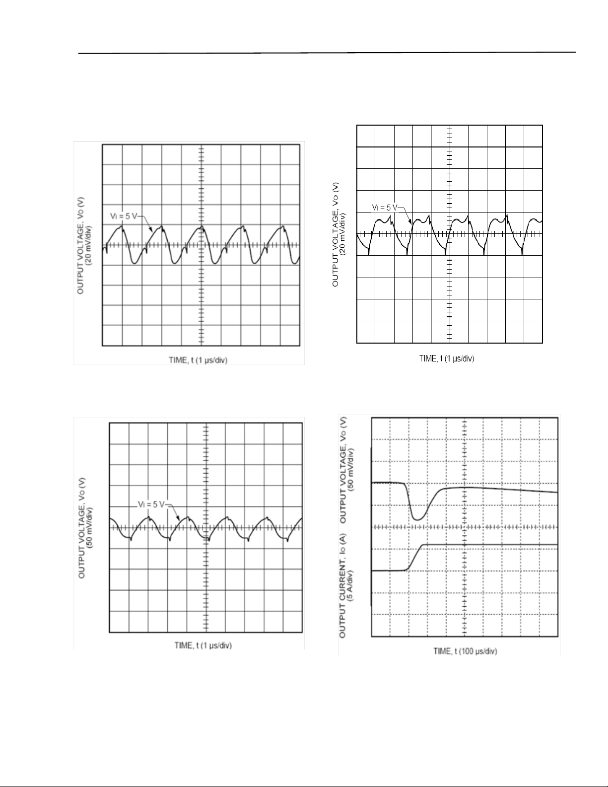
Characteristic Curves
The following figures provide typical characteristics curves at room temperature (TA = 25 °C)
Figure 7. Typical Output Ripple Voltage fo NH020M
(6A Output Current).
Figure 8. Typical Output Ripple Voltage for NH020Y
(6A Output Current).
Figure 9. Typical Output Ripple Voltage for NH020F,G
(6A Output Current).
Figure 10. Typical Transient response to Step load
change from 0% to 100% of I0,max at 5V
Input .
Lineage Power 6
Page 7
Data Sheet
October 14, 2009
5 Vdc Input; 1.5 Vdc to 3.3 Vdc Output; 20 W
NH020-Series Power SIPs:
Characteristic Curves
The following figures provide typical characteristics curves at room temperature (TA = 25 °C)
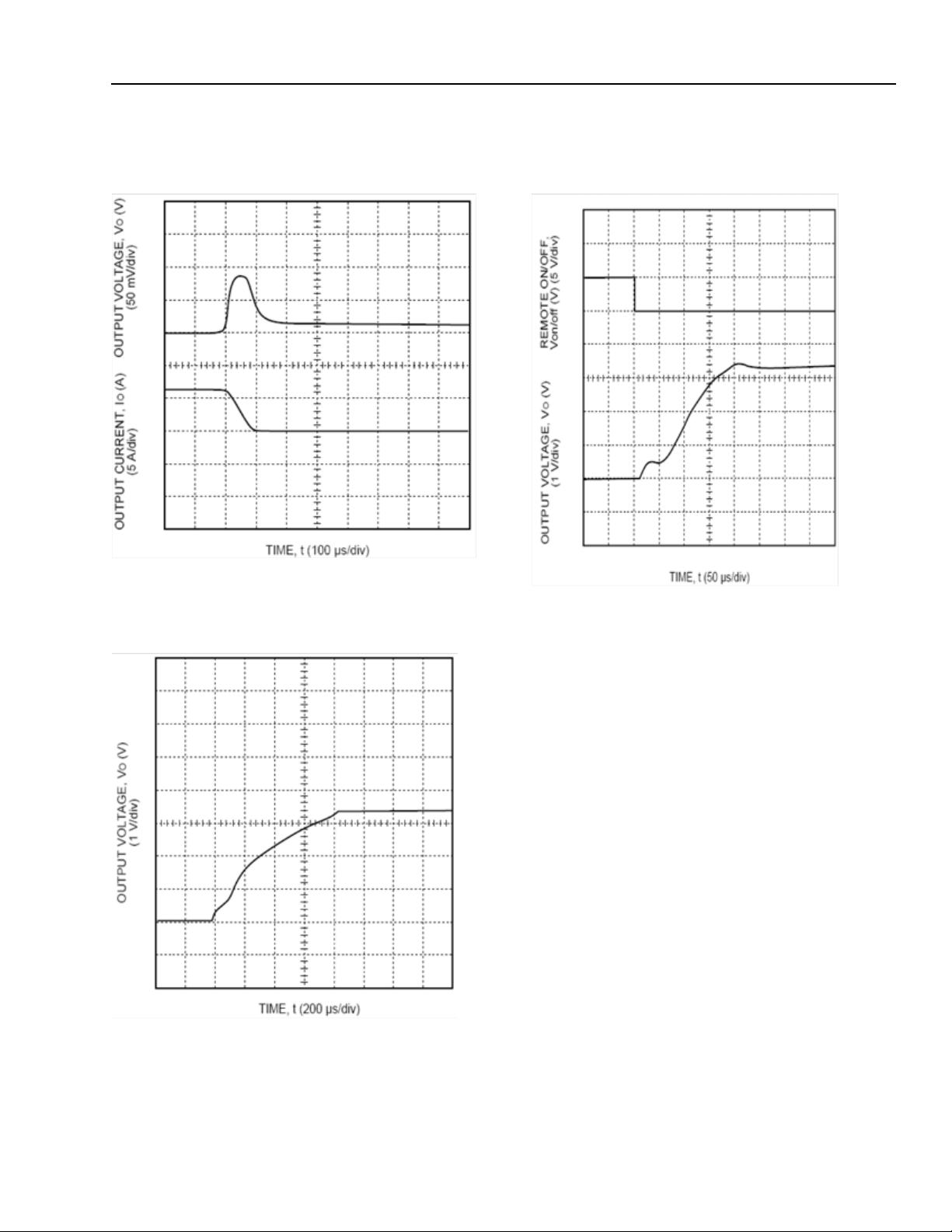
Figure 11. Typical Transient response to Step load
change from 100% to 0% of I0,max at 5V
Input .(Waveform Averaged to remove ripple)
Figure 12. Typical start up Transient at 5V input and 6A
output.
Figure 13. Typical start -up Transient with remote on/off
at 5V Input and 6A output.
Lineage Power 7
Page 8

Data Sheet
October 14, 2009
NH020-Series Power SIPs:
5 Vdc Input; 1.5 Vdc to 3.3 Vdc Output; 20 W
Test Configurations
TO OSCILLOSCOPE
L
500 nH
C
S
BATTER Y
Note: Measure input reflected ripple current with a simulated source
inductance (L
battery impedance. Measure current as shown above.
TEST) of 500nH. Capacitor CS offsets possible
220 µF
ESR < 0.1 •
@ 20 °C , 100 kH z
Figure 14. Input Reflected Ripple Current Test Setup.
I
(+)
V
I
(–)
V
Design Considerations
Input Source Impedance
The power SIP should be connected to a low ac- impedance
input source. Highly inductive source impedances can affect
the stability of the SIP. Adding external capacitance close to
the input pins of the SIP can reduce the ac impedance and
ensure system stability. The minimum recommended input
capacitance (C1) is a 100 µF electrolytic capacitor (see Figures 17 and 19).
Figure 17. Setup with External Capacitor to Reduce
Input Ripple Voltage .
Note: Scope measurements should be made using a BNC socket,
with a 47 µF tantalum capacitor .Position the load between 51
mm and 76 mm (2 in and 3 in) from the module
Figure 15. Peak-to-Peak Output Ripple Measurement
Test Setup.
Note: All voltage measurements to be taken at the module termi-
nals, as shown above. If sockets are used then Kelvin connections are required at the module terminals to avoid
measurement
errors due to socket contact resistance.
Figure 16. Output Voltage and Efficiency Test Setup.
To reduce the amount of ripple current fed back to the input
supply (input reflected-ripple current), an external input filter
can be added. Up to 10 µF of ceramic capacitance (C2) may
be externally connected to the input of the SIP, provided the
source inductance (LSOURCE) is less than 1 µH (see Figure
17).
To further reduce the input reflected-ripple current, a
filter inductor (LFILTER) can be connected between the supply and the external input capacitors (see Figure 18).
As mentioned above, a 100 µF electrolytic capacitor (C1)
should be added across the input of the SIP to ensure stability of the unit. The electrolytic capacitor should be selected
for ESR and RMS current ratings to ensure safe operation in
the case of a fault condition. Refer to Figure 19 for the
appropriate electrolytic capacitor ratings.
When using a tantalum input capacitor, take care not to
exceed device power rating because of the capacitor’s failure mechanism (for example, a short circuit). The
filter inductor should be rated to handle the maximum power
SIP input current of 6.1 Adc.
If the amount of input reflected-ripple current is unacceptable with an external L-C filter, more capacitance may be
added across the input supply to form a C-L-C filter. For best
results, the filter components should be mounted close to
the power SIP.
–[]I
V
O(+)VO(-)
⎛⎞
η
------------------------------------------------
⎝⎠
V
–[]I
I(+)VI(-)
×
O
×
100×=
I
Lineage Power 8
Page 9

Data Sheet
October 14, 2009
Design Considerations (continued)
Input Source Impedance (continued)
Figure 18. Setup with External Input Filter to Reduce
Input Reflected-Ripple Current and Ensure
Stability.
NH020-Series Power SIPs:
5 Vdc Input; 1.5 Vdc to 3.3 Vdc Output; 20 W
Figure 19. Electrolytic Capacitor ESR and RMS Current
Rating Data.
Safety Considerations
For safety-agency approval of the system in which the power
module is used, the power module must be installed in compliance with the spacing and separation requirements of the
end-use safety agency standard, i.e., UL60950, CSA C22.2
No. 60950-00, and
VDE 0805:2001-12 (IEC60950, 3rd Ed).
For the converter output to be considered meeting the
requirements of safety extra-low voltage (SELV),the input
must meet SELV requirements.
The power module has ELV (extra-low voltage) outputs
when all inputs are ELV.
The input to these units is to be provided with a maximum
10A normal-blow fuse in the unearthed lead.
If an input electrolytic capacitor is to be used, it should be
selected using the design information found in the Design
Considerations section.
Lineage Power 9
Page 10

Data Sheet
October 14, 2009
NH020-Series Power SIPs:
5 Vdc Input; 1.5 Vdc to 3.3 Vdc Output; 20 W
Feature Descriptions
Remote On/Off
To turn the power SIP on and off, the user must supply a
switch to control the voltage at the on/off terminal (Von/off).
The switch can be an open collector pnp transistor connected between the on/off terminal and the VI terminal or its
equivalent (see Figure 20).
During a logic low when the ON/OFF pin is open, the power
SIP is on and the maximum Von/off generated
by the power SIP is 0.3 V. The maximum
allowable leakage current of the switch when
Von/off = 0.3 V and VI = 5.5 V (Vswitch = 5.2 V) is 50 µA.
During a logic high, when Von/off = 2.8 V to 5.5 V, the power
SIP is off and the maximum Ion/off is 10 mA. The switch
should maintain a logic high while sourcing 10 mA.
If not using the remote on/off feature, leave the
ON/OFF pin open.
The SIP has internal capacitance to reduce noise at the ON/
OFF pin. Additional capacitance is not generally needed and
may degrade the start-up characteristics of the SIP.
CAUTION: Never ground the on/off terminal. Ground-
ing the on/off terminal disables an important safety feature and may damage the SIP
or the customer system.
18.23
⎛⎞
Rtrim-down
For the G (2.5 VO) SIP:
trim-down
R
Note: Output voltages below 2.5 V cannot be trimmed
down.
The test results for these configurations are displayed in Figures 21 and 22.
----------------------------- -15–
⎝⎠
O VO adj,–
V
6.975
⎛⎞
------------------------------------- 15–
⎝⎠
2.498 V
O adj,–
kΩ=
kΩ=
Figure 20. Remote On/Off Implementation.
Output Voltage Set-Point Adjustment
(Trim)
Output voltage set-point adjustment allows the output voltage set point to be increased or decreased by connecting an
external resistor between the TRIM pin and either the VO pin
(decrease output voltage) or GND pin (increase output voltage). The trim range for the NH020F is +10%, –16%. The
trim range for the NH020G is ±10% of VO, nom. The trim
range for SIPs that produce less than 2.5 VO is +20%, –0%.
Connecting an external resistor (Rtrim-down) between the
TRIM and VO pin decreases the output voltage set point as
defined in the following equation.
For the F (3.3 VO) SIP:
Figure 21. NH020G Rtrim-down Test Results .
Figure 22. NH020F Rtrim-down Test Results .
Connecting an external resistor (Rtrim-up) between the
TRIM and GND pins increases the output voltage set point
to VO, adj as defined in the following equation:
28
⎛⎞
Rtrim-up
The test results for this configuration are displayed in Figures 23—26.
Leave the TRIM pin open if not using that feature.
----------------------------- -1–
⎝⎠
O adj, VO–
V
kΩ=
Lineage Power 10
Page 11

Data Sheet
October 14, 2009
Feature Descriptions (continued)
Output Voltage Set-Point Adjustment
(Trim)
Figure 23.
(continued)
NH020M Rtrim-up Test Results.
NH020-Series Power SIPs:
5 Vdc Input; 1.5 Vdc to 3.3 Vdc Output; 20 W
Figure 26. NH020F Rtrim-up Test Results .
Overcurrent Protection
To provide protection in a fault condition, the unit is equipped
with internal overcurrent protection. The unit operates normally once the fault condition is removed.
The power module will supply up to 350% of rated current for
less than 1.25 seconds before it enters thermal shutdown.
Figure 24. NH020Y Rtrim-up Test Results.
Overtemperature Protection
To provide additional protection in a fault condition, the unit is
equipped with a nonlatched thermal shutdown circuit. The
shutdown circuit engages when Q1 or Q2 exceeds approximately 110 °C. The unit attempts to restart when Q1 or Q2
cool down and cycles on and off while the fault condition
exists. Recovery from shutdown is accomplished when the
cause of the overtemperature condition is removed.
Figure 25. NH020G Rtrim-up Test Results .
Lineage Power 11
Page 12

Data Sheet
October 14, 2009
Thermal Considerations
To predict the approximate cooling needed for the SIP, determine the power dissipated as heat by the unit for the particular application. Figures 29—32 show typical heat dissipation
for the SIP over a range of output currents.
NH020-Series Power SIPs:
5 Vdc Input; 1.5 Vdc to 3.3 Vdc Output; 20 W
Figure 29. NH020M Power Dissipation vs. Output
current.
Note: Dimensions are in millimeters and (inches).
Figure 27. Thermal Test Setup.
Proper cooling can be verified by measuring the power SIP’s
temperature at lead 7 of Q31 as shown in Figure 28.
Figure 28. Temperature Measurement Location.
The temperature at this location should not exceed 115 °C.
The output power of the SIP should not exceed the rated
power for the SIP as listed in the Ordering Information table.
Convection Requirements for Cooling
To predict the approximate cooling needed for the SIP, determine the power dissipated as heat by the unit for the particular application. Figures 29—32 show typical heat dissipation
for the SIP over a range of output currents.
Figure 30. NH020Y Power Dissipation vs. Output
Current.
Figure 31. NH020G Power Dissipation vs. Output
Current.
Lineage Power 12
Page 13

Data Sheet
October 14, 2009
Figure 32. NH020F Power Dissipation vs. Output
Current.
With the known heat dissipation and a given local ambient
temperature, the minimum airflow can be chosen from the
derating curves in Figure 33.
NH020-Series Power SIPs:
5 Vdc Input; 1.5 Vdc to 3.3 Vdc Output; 20 W
Figure 33. Power Derating vs. Loca l Ambient
Temperature and Air Velocity
For example, if the unit dissipates 2.0 W of heat, the minimum airflow in an 80 °C environment is 1.0 m/s
(200 ft./min.).
Keep in mind that these derating curves are approximations
of the ambient temperatures and airflows require d to keep
the power SIP temperature below its maximum rating. Once
the SIP is assembled in the actual system, the SIP’s temperature should be checked as shown in Figure 28 to ensure it
does not exceed 115 °C.
.
Layout Considerations
Copper paths must not be routed between pins 2 and 3 and
pins 7 and 8.
Lineage Power 13
Page 14

Data Sheet
October 14, 2009
Through-Hole Lead-Free Soldering Information
The RoHS-compliant through-hole products use the SAC
(Sn/Ag/Cu) Pb-free solder and RoHS-compliant components. They are designed to be processed through single or
dual wave soldering machines. The pins have an RoHScompliant finish that is compatible with both Pb and Pb-free
wave soldering processes. A maximum preheat rate of 3°C/s
is suggested. The wave preheat process should be such
that the temperature of the power module board is kept
below 210°C. For Pb solder, the recommended pot temperature is 260°C, while the Pb-free solder pot is 270°C max.
Not all RoHS-compliant through-hole products can be processed with paste-through-hole Pb or Pb-free reflow process. If additional information is needed, please consult with
your Tyco Electronics Power System representative for more
details.
Post Solder Cleaning and Drying Considerations
Post solder cleaning is usually the final circuit-board
assembly process prior to electrical board testing. The result
of inadequate cleaning and drying can affect both the
reliability of a power module and the testability of the
finished circuit-board assembly. For guidance on appropriate
soldering, cleaning and drying procedures, refer to Tyco
Electronics Board Mounted Power Modules: Soldering and
Cleaning Application Note (AP01-056EPS).
NH020-Series Power SIPs:
5 Vdc Input; 1.5 Vdc to 3.3 Vdc Output; 20 W
Solder Ball and Cleanliness Requirements
The open frame (no case or potting) power module will meet
the solder ball requirements per J-STD-001B. These
requirements state that solder balls must neither be loose
nor violate the power module minimum electrical spacing.
The cleanliness designator of the open frame power module
is C00 (per J specification).
Lineage Power 14
Page 15
Data Sheet
October 14, 2009
5 Vdc Input; 1.5 Vdc to 3.3 Vdc Output; 20 W
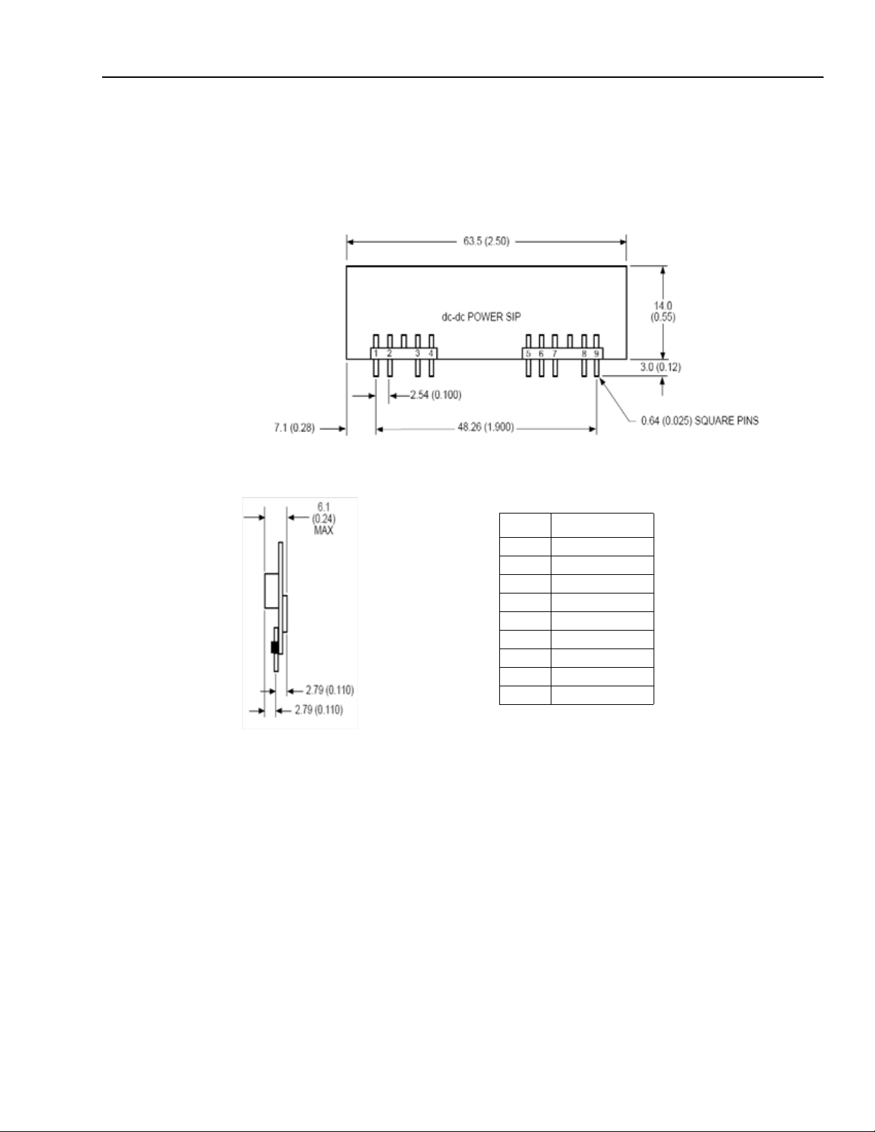
Outline Diagram for Through-Hole Module
Dimensions are in millimeters and (inches).
Tolerances: x.x mm ± 0.5 mm (x.xx in. ± 0.02 in.) [unless otherwise indicated]
x.xx mm ± 0.25 mm (x.xxx in. ± 0.010 in.)
Front View
NH020-Series Power SIPs:
Side View
Pin Function
1VO
2VO
3VO
4GND
5GND
6VI
7VI
8TRIM
9ON/OFF
Lineage Power 15
Page 16
Data Sheet
October 14, 2009
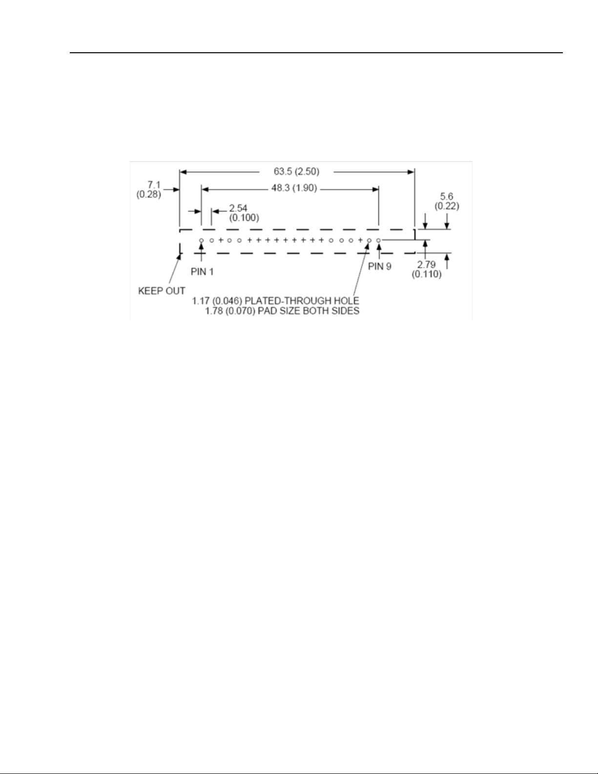
Recommended Hole Pattern
Component-side footprint.
Dimensions are in millimeters and (inches).
NH020-Series Power SIPs:
5 Vdc Input; 1.5 Vdc to 3.3 Vdc Output; 20 W
Note: No copper should be placed between pins 2 and 3 and pins 7 and 8.
Lineage Power 16
Page 17
Data Sheet
October 14, 2009
5 Vdc Input; 1.5 Vdc to 3.3 Vdc Output; 20 W
NH020-Series Power SIPs:
Ordering Information
Please contact your Tyco Electronics’ Sales Representative for pricing, availability and optional features.
Table 1. Device Codes
Input Voltage Output Voltage Output Current Device Code Comcodes
5 V 1.5 V 9 W NH020M 107870065
5 V 1.
5 V 2.5 V 15 W NH020G 107917114
5 V 3.
5V 3.3V 20W NH020FZ CC109114121
5 V 2.5 V 1
5 V 1.8 V 10.8 W NH020Y2Z CC109102761
nal features can be ordered using the suffixes shown below. The suffixes follow the last letter of the Product Code and are
Optio
placed in descending alphanumerical order.
Table 2. Device Options
Option Suffix
Tight tolerance output
t available on the NH020G)
(no
0 °C operation 5
–4
RoHS Compliant -Z
8 V 10.8 W NH020Y TBD
3 V 20 W NH020F 107221145
5 W NH020GZ CC109102753
2
A sia-Pa ci fic He
Tel: +6
5 6 41 6 4283
Eu ro pe, Middle -East an d Afric a He ad qu arters
9 898 780 672 80
World W ide Headqu arte r s
Lineag e Po w er Co rp or ation
6
iloh Road, Plano, TX 75 07 4, U S A
01 Sh
+1-800 -5
(Outsid e U .S.A .: +1- 97 2-244-9
ww w.l ine ag ep ower .co m
e-m ail: te ch sup p
Lineage Pow er re serves th e righ t to m ake cha nges to th e product(s) or info rma tion con tained h erein with out notice. No liab ility is a ss umed as a res ult of their use or
ap plica tio
Lineage Power DC-DC products are protected under various patents. Information on these patents is available at www.lineagepower.com/patents.
© 2 009 L in
26-78 19
428)
ort1@ li n ea gepowe r .co m
n. No rights u nd er any patent acc ompany th e sale o f any s uch produ ct(s) o r info rmati on.
ea ge Powe r Co rporati on, (P lan o, Texas) Al l Inte rnational Righ ts Res erved.
Tel: +4
India Headqu arter s
Tel: +9
1 8 0 28411633
ad qu a rt ers
October 2009
PDF Name:DS00-128EPS (Replaces DS00-127EPS)
 Loading...