

Page 1
Data Sheet
September 7, 2011
TM
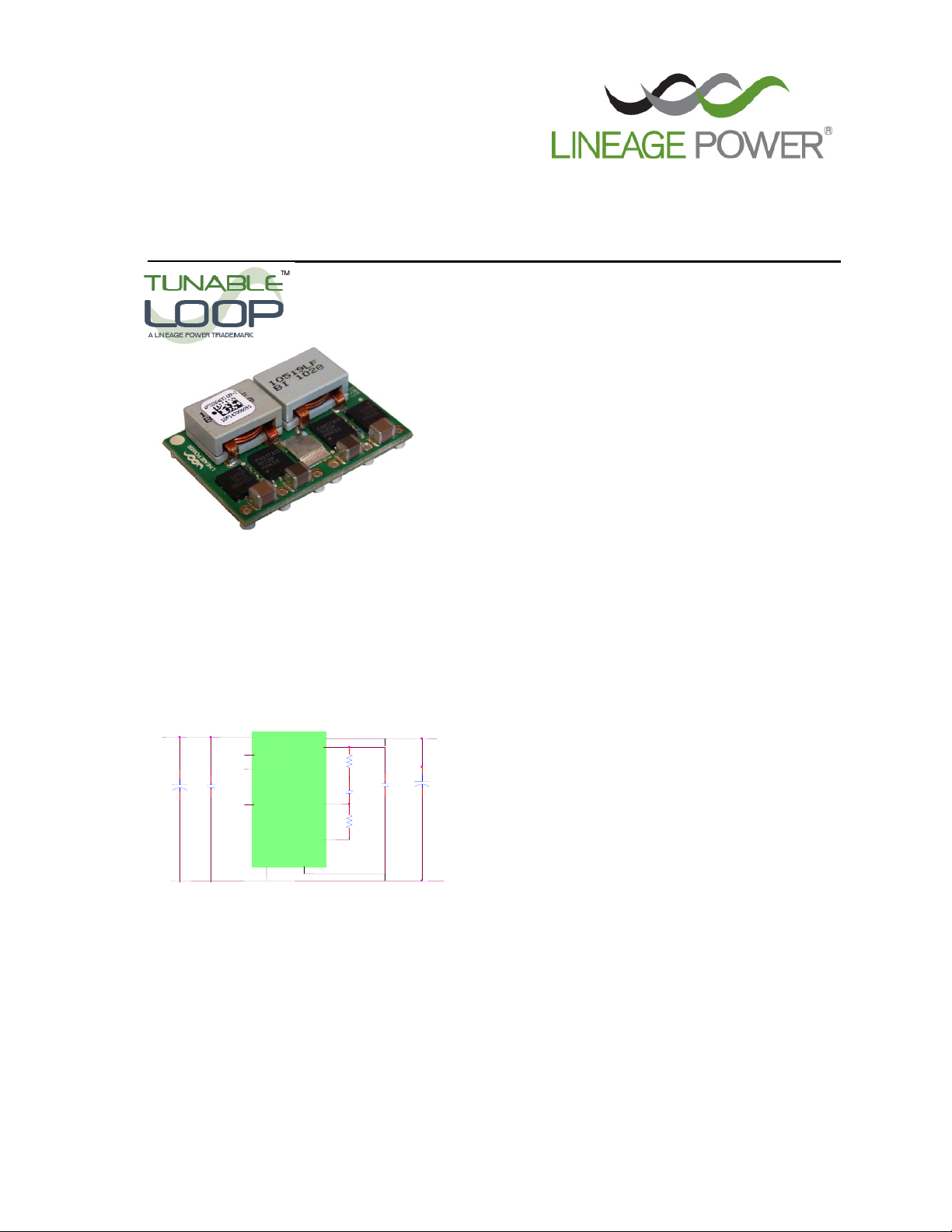
GigaTLynx
Non-isolated Power Modules:
4.5Vdc – 14Vdc input; 0.7Vdc to 2Vdc, 50A Output
Applications
Distributed power architectures
Intermediate bus voltage applications
Industrial applications
Telecommunications equipment
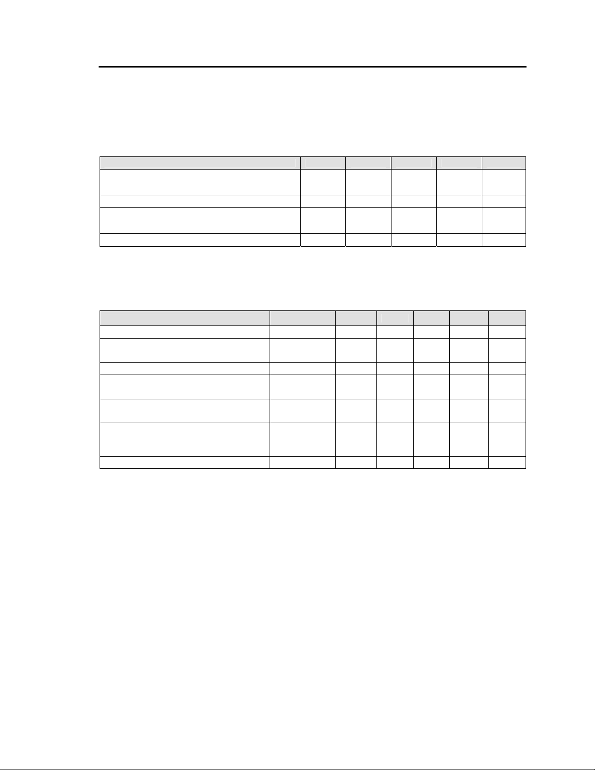
Vin+
VIN
VOUT
SENSE+
SENSE-
SENSE-
TRIM+
TRIM-
PGOOD
SEQ
+
CI2
MODULE
CI1
ON/OFF
GND
Vout+
RTUNE
CTUNE
RTrim
Features
Compliant to RoHS EU Directive 2002/95/EC
(-Z versions)
Compliant to RoHS EU Directive 2002/95/EC with
lead solder exemption (non-Z versions)
Input voltage from 4.5Vdc to 14Vdc
Output voltage programmable from 0.7 Vdc to
2.0Vdc via external resistor
Output current up to 50A
Tunable control loop for fast transient response
True differential remote sense
Negative remote On/Off logic
Output voltage sequencing (EZ-SEQUENCE
TM
)
Output over current protection (non-latching)
Over temperature protection
Monotonic startup under pre-bias conditions
Parallel operation with active current sharing
Small size and low profile:
33 mm x 22.9 mm x 10 mm (max.)
(1.3 in x 0.9 in x 0.393 in (max.))
+
CO2
CO1
Wide operating temperature range [-40°C to
105°C(Ruggedized: -D), 85°C(Regular)]
nd
UL* 60950-1, 2
Ed. Recognized, CSA† C22.2 No.
60950-1-07 Certified, and VDE‡ (EN60950-1, 2nd
Ed.) Licensed
ISO** 9001 and ISO 14001 certified manufacturing
facilities
Description
The GigaTLynxTM series of power modules are non-isolated dc-dc converters that can deliver up to 50A of output
current. These modules operate over a wide range of input voltage (V
regulated output voltage from 0.7Vdc to 2.0Vdc, programmable via an external resistor. Features include remote
On/Off, adjustable output voltage, over current and over temperature protection, output voltage sequencing and
paralleling. The Ruggedized version (-D) is capable of operation up to 105°C and withstand high levels of shock
and vibration. The Tunable Loop
TM
feature, allows the user to optimize the dynamic response of the converter to
match the load with reduced amount of output capacitance leading to savings on cost and PWB area.
*
UL is a registered trademark of Underwriters Laborat ories, Inc.
†
CSA is a registered trademark of Canadian Standards A ssociation.
‡
VDE is a trademark of Verband Deutscher Elektrotechniker e.V.
** ISO is a registered trademark of the Internation al Organization of Standards
= 4.5Vdc-14Vdc) and provide a precisely
IN
Document No: DS010-005 ver. 1.23
PDF name: APTS050A0X_ds.pdf
Page 2
Data Sheet
September 7, 2011
GigaTLynx
4.5 – 14Vdc input; 0.7Vdc to 2.0Vdc, 50A Output
TM
SMT Non-isolated Power Modules:
Absolute Maximum Ratings
Stresses in excess of the absolute maximum ratings can cause permanent damage to the device. These are
absolute stress ratings only, functional operation of the device is not implied at these or any other conditions in
excess of those given in the operations sections of the data sheet. Exposure to absolute maximum ratings for
extended periods can adversely affect the device reliability.
Parameter Device Symbol Min Max Unit
Input Voltage All V
Continuous
IN
-0.3 14 Vdc
Sequencing pin voltage All VsEQ -0.3 4 Vdc
Operating Ambient Temperature All T
(see Thermal Considerations section) -D version T
Storage Temperature All T
A
A
stg
-40 85 °C
-40 105 °C
-55 125 °C
Electrical Specifications
Unless otherwise indicated, specifications apply over all operating input voltage, resistive load, and temperature
conditions.
Parameter Device Symbol Min Typ Max Unit
Operating Input Voltage Vo,set ≤ 2.0 VIN 4.5
Maximum Input Current All I
(VIN= V
IN, min
to V
IN, max
, IO=I
) 26
O, max
Inrush Transient All
Input No Load Current V
(VIN = V
, Io = 0, module enabled) V
IN, nom
= 0.7Vdc I
O,set
= 1.8Vdc I
O,set
Input Stand-by Current All I
(VIN = V
, module disabled)
IN, nom
IN,max
2
I
t
IN,No load
IN,No load
IN,stand-by
Adc
1
73.4 mA
136 mA
1.3 mA
⎯
Input Reflected Ripple Current, peak-to-peak
(5Hz to 20MHz, 1μH source impedance; V
V
= I
IN, max, IO
; See Test configuration section)
Omax
IN, min
to
All 73 mAp-p
Input Ripple Rejection (120Hz) All 50 dB
CAUTION: This power module is not internally fused. An input line fuse must always be used.
This power module can be used in a wide variety of applications, ranging from simple standalone operation to an
integrated part of sophisticated power architecture. To preserve maximum flexibility, internal fusing is not included;
however, to achieve maximum safety and system protection, always use an input line fuse. The safety agencies
require a surface mount, fast acting fuse (ie. Littelfuse 456030 series) with a maximum rating of 30 A (see Safety
Considerations section). Based on the information provided in this data sheet on inrush energy and maximum dc
input current, the same type of fuse with a lower rating can be used. Refer to the fuse manufacturer’s data sheet for
further information.
14 Vdc
2
A
s
LINEAGE POWER 2
Page 3
Data Sheet
September 7, 2011
GigaTLynx
4.5 – 14Vdc input; 0.7Vdc to 2.0Vdc, 50A Output
TM
SMT Non-isolated Power Modules:
Electrical Specifications (continued)
Parameter Device Symbol Min Typ Max Unit
Output Voltage Set-point
(V
IN=VIN,nom
, IO=I
O, nom
, T
=25°C)
ref
All V
Output Voltage All V
(Over all operating input voltage, resistive load,
and temperature conditions until end of life)
Adjustment Range All V
Selected by an external resistor
O, set
O, set
O
-1.0
-2.0
⎯
⎯
0.7 2.0 Vdc
+1.0 % V
+2.0 % V
O, set
O, set
Output Regulation
Line (VIN=V
Load (IO=I
Temperature (T
IN, min
O, min
to V
to I
ref=TA, min
) All
IN, max
) All
O, max
to T
) All ⎯ 8 mV
A, max
⎯
⎯
5 mV
8 mV
Remote Sense Range All 0.5 Vdc
Output Ripple and Noise on nominal output
(VIN=V
Cout = 1μF ceramic//2x10μF ceramic
Peak-to-Peak (5Hz to 20MHz bandwidth) All
External Capacitance
IN, nom
and IO=I
O, min
1
to I
O, max
⎯
50 mV
pk-pk
Without the Tunable LoopTM
ESR ≥ 1 mΩ All C
ESR ≥ 10 mΩ All C
O, max
O, max
⎯ ⎯
⎯ ⎯
1200 μF
10000 μF
With the Tunable Loop
ESR ≥ 1 mΩ All C
ESR ≥ 10 mΩ All C
Output Current All I
Output Current Limit Inception (Hiccup Mode ) All I
Output Short-Circuit Current All I
(VO≤250mV) ( Hiccup Mode )
Efficiency V
VIN= 12V, TA=25°C V
IO=I
O, max , VO
= V
V
O,set
= 0.7Vdc η 81.1 %
O, set
= 1.2Vdc η 87.0 %
O,set
= 1.8Vdc η 90.1 %
O,set
Switching Frequency All f
O, max
O, max
o
O, lim
O, s/c
sw
⎯ ⎯
⎯ ⎯
0 50A Adc
⎯
⎯
180
5.5
⎯
260
20000 μF
20000 μF
⎯
⎯
⎯
% I
Adc
kHz
o
General Specifications
Parameter Min Typ Max Unit
Telcordia Issue 2, Method I, Case 3, Calculated MTBF (IO=I
T
=40°C)
A
Weight
O, max
,
⎯
4,755,661
Hours
14.22 (0.5) g (oz.)
__________________________________
External capacitors may require using the new Tunable Loop
getting the best transient response. See the Tunable Loop
LINEAGE POWER 3
TM
feature to ensure that the module is stable as well as
TM
section for details.
Page 4
Data Sheet
September 7, 2011
GigaTLynx
4.5 – 14Vdc input; 0.7Vdc to 2.0Vdc, 50A Output
TM
SMT Non-isolated Power Modules:
Feature Specifications
Unless otherwise indicated, specifications apply over all operating input voltage, resistive load, and temperature
conditions. See Feature Descriptions for additional information.
Parameter Device Symbol Min Typ Max Unit
On/Off Signal Interface
(VIN=V
Signal referenced to GND)
Logic High (On/Off pin open – Module OFF)
Input High Current All IIH
Input High Voltage All VIH
Logic Low (Module ON)
Input Low Current All IIL
Input Low Voltage All VIL
Turn-On Delay and Rise Times
(IO=I
Case 1: On/Off input is set to Logic Low (Module
ON) and then input power is applied (delay from
instant at which V
Case 2: Input power is applied for at least one second
and then the On/Off input is set to logic Low (delay from
instant at which Von/Off=0.3V until Vo=10% of Vo, set)
Output voltage Rise time (time for Vo to rise from 10%
of V
Output voltage overshoot – Startup ― 3.0 % V
IO= I
Over Temperature Protection All T
(See Thermal Consideration section)
Sequencing Slew rate capability All dVSEQ/dt — 2 V/msec
(V
IN, min
Sequencing Delay time (Delay from V
to application of voltage on SEQ pin) All TsEQ-delay 10 msec
Tracking Accuracy Power-up (2V/ms) All VSEQ –Vo 100 200 mV
Power-down (1V/ms) VSEQ –Vo 200 400 mV
Input Undervoltage Lockout
Turn-on Threshold All
Turn-off Threshold All 4.04 V
Hysteresis All
Forced Load Share Accuracy All
Number of units in Parallel All
PGOOD (Power Good)
Internal pull-up, V
Overvoltage threshold for PGOOD All 112.5 %V
Undervoltage threshold for PGOOD All
IN, min
O, max , VIN
to V
= V
; open collector or equivalent,
IN, max
= 25 oC, )
IN, nom, TA
0.5
3.0
⎯
⎯
3.3 mA
V
IN, max
⎯ ⎯
-0.3
⎯
200 µA
0.6 V
V
All Tdelay ― 4.8 ― msec
=V
IN
until Vo=10% of Vo,set)
IN, min
All Tdelay ― 4.8 ― msec
All Trise
o,set to 90% of Vo, set)
; VIN = 4.5 to 14Vdc, TA = 25 oC
O, max
ref
to V
IN, max
; I
to I
O, min
(V
PGOOD
IN, min
VSEQ < Vo)
O, max
IN, min
to V
All
IN, max
; I
- I
O, min
VSEQ < Vo)
O, max
― 3.6 ― msec
⎯
125
⎯
4.26 V
0.22 Vdc
⎯
10 % Io
5
5 V
87.5 %V
°C
O, set
O, set
O, set
LINEAGE POWER 4
Page 5
Data Sheet
OUTPUT
CURRENT
OUTPUT
VOLTAGE
September 7, 2011
GigaTLynx
4.5 – 14Vdc input; 0.7Vdc to 2.0Vdc, 50A Output
TM
SMT Non-isolated Power Modules:
Characteristic Curves
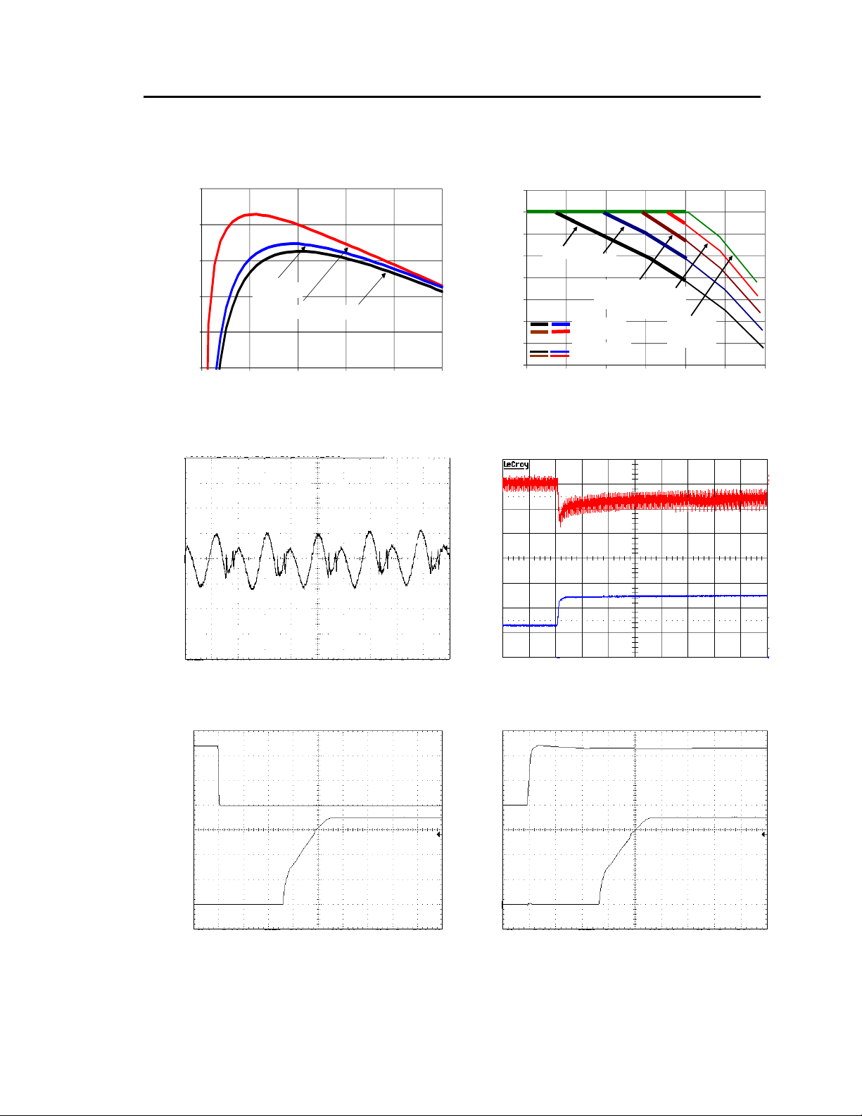
The following figures provide typical characteristics for the 12V Giga TLynxTM 50A at 0.7Vo and at 25oC.
95
90
85
80
75
Vin=12V
Vin=4.5V
Vin=14V
EFFICIENCY, η (%)
70
0 1020304050
OUTPUT CURRENT, IO (A) AMBIENT TEMPERATURE, TA OC
Figure 1. Converter Efficiency versus Output Current.
(V) (10mV/div)
O
V
OUTPUT VOLTAGE
TIME, t (1μs/div)
Figure 3. Typical output ripple and noise (V
I
o,max).
IN = 12V, Io =
55
50
45
40
35
30
25
20
OUTPUT CURRENT, Io (A)
15
NC
0.5m/s
(100LFM)
1m/s
(
200LFM
Standard Part
(85 C)
Ruggedized (D)
Part (105 C)
)
(300LFM)
1.5m/s
2m/s
(400LFM)
45 55 65 75 85 95 105
Figure 2. Derating Output Current versus Ambient
Temperature and Airflow.
(V) (10mV/div)
O
(A) (20Adiv) V
O
I
TIME, t (0.2ms /div)
Figure 4. Transient Response to Dynamic Load
Change from 50% to 100% at 12Vin, Cext =5x47uF+
+22x330uFpolymer,CTune=330nF,RTune=100ohms
(V) (5V/div)
ON/OFF
(V) (200mV/div) V
O
OUTPUT VOLTAGE ON/OFF VOLTAGE
V
TIME, t (2ms/div)
Figure 5. Typical Start-up Using On/Off Voltage (I
I
o,max).
o =
(V) (5V/div)
IN
(V) (200mV/div) V
O
OUTPUT VOLTAGE INPUT VOLTAGE
V
TIME, t (2ms/div)
Figure 6. Typical Start-up Using Input Voltage (V
12V, I
o = Io,max).
IN =
LINEAGE POWER 5
Page 6
Data Sheet
OUTPUT
CURRENT
OUTPUT
VOLTAGE
September 7, 2011
GigaTLynx
4.5 – 14Vdc input; 0.7Vdc to 2.0Vdc, 50A Output
TM
SMT Non-isolated Power Modules:
Characteristic Curves
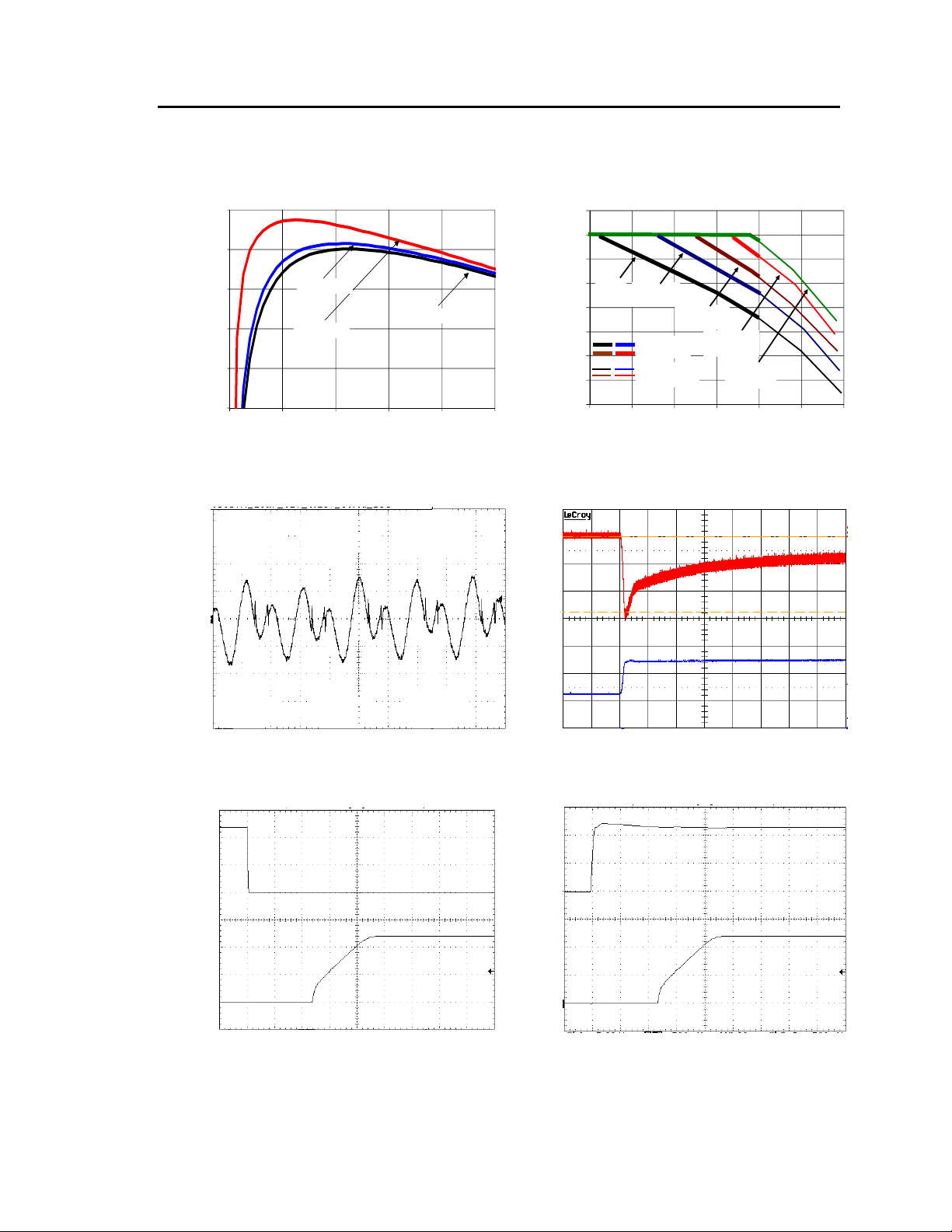
The following figures provide typical characteristics for the 12V Giga TLynxTM 50A at 1.2 Vo and at 25oC.
95
90
85
80
75
Vin=12V
Vin=14V
Vin=4.5V
EFFICIENCY, η (%)
70
0 1020304050
OUTPUT CURRENT, IO (A) AMBIENT TEMPERATURE, TA OC
Figure 7. Converter Efficiency versus Output Current.
(V) (10mV/div)
O
V
OUTPUT VOLTAGE
TIME, t (1μs/div)
Figure 9. Typical output ripple and noise (V
I
o,max).
IN = 12V, Io =
55
50
45
40
NC
0.5m/s
35
30
25
20
OUTPUT CURRENT, Io (A)
15
(100LFM)
Standard Part
(85 C)
Ruggedized (D)
Part (105 C)
1m/s
(200LFM)
1.5m/s
(300LFM)
(400LFM)
2m/s
45 55 65 75 85 95 105
Figure 8. Derating Output Current versus Ambient
Temperature and Airflow.
(V) (10mV/div)
O
,
(A) (20Adiv) V
O
I
TIME, t (0.1ms /div)
Figure 10. Transient Response to Dynamic Load
Change from 50% to 100% at 12Vin, Cext =5x47uF+
+13x330uFpolymer,CTune=120nF,RTune=180ohms
(V) (5V/div)
ON/OFF
(V) (500mV/div) V
O
OUTPUT VOLTAGE ON/OFF VOLTAGE
V
Figure 11. Typical Start-up Using On/Off Voltage (Io =
I
o,max).
TIME, t (2 ms/div) TIME, t (2 ms/div)
(V) (5V/div)
IN
(V) (500mV/div) V
O
OUTPUT VOLTAGE INPUT VOLTAGE
V
Figure 12. Typical Start-up Using Input Voltage (V
12V, I
o = Io,max).
IN =
LINEAGE POWER 6
Page 7
Data Sheet
OUTPUT
CURRENT
OUTPUT
VOLTAGE
September 7, 2011
GigaTLynx
4.5 – 14Vdc input; 0.7Vdc to 2.0Vdc, 50A Output
TM
SMT Non-isolated Power Modules:
Characteristic Curves
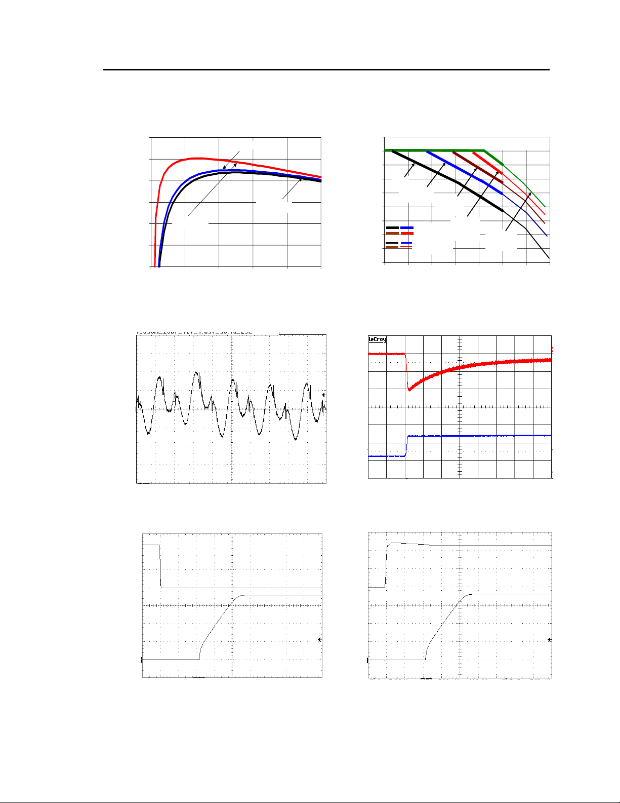
The following figures provide typical characteristics for the 12V Giga TLynxTM 50A at 1.8 Vo and at 25oC.
EFFICIENCY, η (%)
100
95
90
85
80
75
70
0 1020304050
Vin=4.5V
Vin=12V
Vin=14V
OUTPUT CURRENT, IO (A) AMBIENT TEMPERATURE, TA OC
Figure 13. Converter Efficiency versus Output Current.
(V) (10mV/div)
O
V
OUTPUT VOLTAGE
TIME, t (1μs/div)
Figure 15. Typical output ripple and noise (V
I
o,max).
IN = 12V, Io =
55
Output Voltage set to 2V for thermal derating curve
50
45
40
NC
35
30
25
20
15
OUTPUT CURRENT, Io (A)
10
0.5m/s
(100LFM)
(200LFM)
Standard Part
(85 C)
Ruggedized (D)
Part (105 C)
1m/s
1.5m/s
(300LFM)
2m/s
(400LFM)
35 45 55 65 75 85 95 105
Figure 14. Derating Output Current versus Ambient
Temperature and Airflow.
(V) (20mV/div)
O
,
(A) (20Adiv) V
O
I
TIME, t (0.1ms /div)
Figure 16. Transient Response to Dynamic Load
Change from 50% to 100% at 12Vin, Cext =5x47uF+
+8x330uFpolymer,CTune=47nF,RTune=220ohms
(V) (5V/div)
ON/OFF
(V) (500mV/div) V
O
OUTPUT VOLTAGE ON/OFF VOLTAGE
V
TIME, t (2 ms/div) TIME, t (2 ms/div)
Figure 17. Typical Start-up Using On/Off Voltage (Io =
I
o,max).
(V) (5V/div)
IN
(V) (500mV/div) V
O
OUTPUT VOLTAGE INPUT VOLTAGE
V
Figure 18. Typical Start-up Using Input Voltage (V
12V, I
o = Io,max).
LINEAGE POWER 7
IN =
Page 8

Data Sheet
September 7, 2011
GigaTLynx
4.5 – 14Vdc input; 0.7Vdc to 2.0Vdc, 50A Output
TM
SMT Non-isolated Power Modules:
Test Configurations
TO OSCILLOSCOPE
L
TEST
1μH
CS 1000μF
BATTERY
NOTE: Measure input reflected ripple current with a simulated
source inductance (L
possible battery im pedance. Measure curre nt as shown
above.
Electrolytic
E.S.R.<0.1Ω
@ 20°C 100k Hz
) of 1μH. Capa citor CS offsets
TEST
Figure 19. Input Reflected Ripple Current Test Setup.
COPPER STRIP
Vo+
0.1uF
COM
NOTE : All volt age measurem ents to be t aken at the module
termin als, as shown ab ove. If soc kets ar e use d then
Kelvin connections are required at the module terminals
to av oid me asur ement er rors due to socket contac t
resistance.
10uF
GROUND PLANE
Figure 20. Output Ripple and Noise Test Setup.
R
R
contact
distribution
R
R
contact
distribution
NOTE: All volt age meas urements to be taken at th e module
terminals , as shown above. If sock ets are us ed then
Kelvin c onnections are required at t he module termi nals
to avoid measur ement err ors due to soc ket contact
resistance.
VIN(+)
V
IN
COM
Figure 21. Output Voltage and Efficiency Test Setup.
V
. I
O
Efficiency
=
η
VIN. I
O
IN
COM
V
O
2x100μF
Tantalum
CURRENT PROBE
CIN
SCO PE U SIN G
BNC SOC KET
R
V
O
R
x 100 %
VIN(+)
COM
RESISTIVE
LOAD
contactRdistribution
R
contactRdistribution
LOAD
Design Considerations
Input Filtering
The Giga TLynxTM module should be connected to a
low ac-impedance source. A highly inductive source
can affect the stability of the module. An input
capacitance must be placed directly adjacent to the
input pin of the module, to minimize input ripple voltage
and ensure module stability.
To minimize input voltage ripple, ceramic capacitors
are recommended at the input of the module. Figure 22
shows the input ripple voltage for various output
voltages at maximum load current with 2x22 µF or
4x22 µF or 4x47 µF ceramic capacitors and an input of
12V.
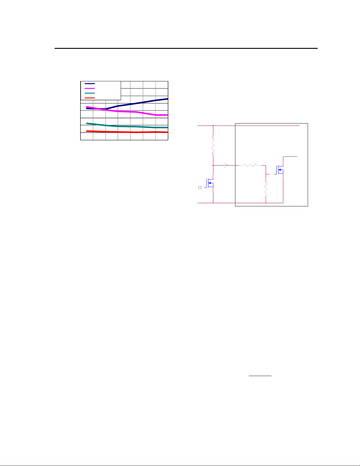
250
225
200
175
150
125
100
75
50
Input Ripple Voltage (mVp-p)
Output Voltage (Vdc)
Figure 22. Input ripple voltage for various output
voltages with 2x22 µF, 4x22 µF or 4x47 µF ceramic
capacitors at the input (maximum load). Input voltage
is 12V
Output Filtering
The Giga TLynxTM modules are designed for low output
ripple voltage and will meet the maximum output ripple
specification with 0.1 µF ceramic and 10 µF ceramic
capacitors at the output of the module. However,
additional output filtering may be required by the system
designer for a number of reasons. First, there may be a
need to further reduce the output ripple and noise of the
module. Second, the dynamic response characteristics
may need to be customized to a particular load step
change.
To reduce the output ripple and improve the dynamic
response to a step load change, additional capacitance at
the output can be used. Low ESR polymer and ceramic
capacitors are recommended to improve the dynamic
response of the module. Figure 23
information for different external capacitance values at
various Vo and for full load currents. For stable
of the module, limit the capacitance to less than the
maximum output capacitance as specified in the electrical
specification table. Optimal performance of the module
can be
achieved by using the Tunable Loop feature described
later in this data sheet.
2x22uF
4x22uF
4x47uF
1 1.25 1.5 1.75 2
provides output ripple
operation
LINEAGE POWER 8
Page 9
Data Sheet
_
September 7, 2011
Feature Descriptions
80
70
60
50
40
30
Rippl e (mVp-p)
20
10
0
0.6 0.8 1 1.2 1.4 1.6 1.8 2
Figure 23. Output ripple voltage for various output
voltages with external 2x10 µF, 2x47 µF, 4x47 µF or
8x47 µF ceramic capacitors at the output (50A load).
Input voltage is 12V.
2x10uF Ext Cap
2x47uF Ext Cap
4x47uF Ext Cap
8x47uF Ext Cap
Output Voltage(Volts)
Safety Considerations
For safety agency approval the power module must be
installed in compliance with the spacing and separation
requirements of the end-use safety agency standards,
i.e., UL 60950-1 2nd, CSA C22.2 No. 60950-1-07, DIN
EN 60950-1:2006 + A11 (VDE0805 Teil 1 + A11):200911; EN 60950-1:2006 + A11:2009-03.
For the converter output to be considered meeting the
requirements of safety extra-low voltage (SELV), the
input must meet SELV requirements. The power module
has extra-low voltage (ELV) outputs when all inputs are
ELV. The input to these units is to be provided with a
surface mount, fast acting fuse (ie. Littelfuse 456030
series) with a maximum rating of 30A in the positive input
lead.
Remote On/Off
The GigaTLynxTM SMT power modules feature a On/Off
pin for remote On/Off operation. If not using the On/Off
pin, connect the pin to ground (the module will be ON).
The On/Off signal (V
circuit configuration for remote On/Off operation of the
module using the On/Off pin is shown in Figure 24.
During a Logic High on the On/Off pin (transistor Q1 is
OFF), the module remains OFF. The external resistor R1
should be chosen to maintain 3.0V minimum on the
On/Off pin to ensure that the module is OFF when
transistor Q1 is in the OFF state. Suitable values for R1
are 4.7K for input voltage of 12V and 3K for 5Vin. During
Logic-Low when Q1 is turned ON, the module is turned
ON.
The On/Off pin can also be used to synchronize the
output voltage start-up and shutdown of multiple modules
in parallel. By connecting On/Off pins of multiple
modules, the output start-up can be synchronized (please
refer to characterization curves).
LINEAGE POWER
) is referenced to ground. The
on/off
9
GigaTLynx
TM
SMT Non-isolated Power Modules:
4.5 – 14Vdc input; 0.7Vdc to 2.0Vdc, 50A Output
Overcurrent Protection
To provide protection in a fault (output overload)
condition, the unit should be equipped with internal
current-limiting circuitry and can endure current limiting
continuously. At the point of current-limit inception, the
unit enters hiccup mode. The unit should operate
normally once the output current is brought back into its
specified range.
VIN+
R1
I
ON/OFF
GND
ON/OFF
V
ON/OFF
Q1
Figure 24. Remote On/Off Implementation
using ON/OFF .
Overtemperature Protection
To provide protection in a fault condition, the unit is
equipped with a thermal shutdown circuit. The unit will
shutdown if the overtemperature threshold of 125
exceeded at the thermal reference point T
shutdown is not intended as a guarantee that the unit will
survive temperatures beyond its rating. Once the unit
goes into thermal shutdown it will then wait to cool before
attempting to restart.
Input Undervoltage Lockout
At input voltages below the input undervoltage lockout
limit, module operation will be disabled. The module will
begin to operate at an input voltage above the
undervoltage lockout turn-on threshold.
Output Voltage Programming
The output voltage of the GigaTLynxTM can be
programmable to any voltage from 0.7 Vdc to 2.0Vdc by
connecting a single resistor (shown as Rtrim in Figure 25)
between the TRIM+ and TRIM pins of the module. The
following equation will be used to set the output voltage of
the module:
By using a ±0.5% tolerance trim resistor with a TC of
±100ppm, a set point tolerance of ±1.5% can be achieved
as specified in the electrical specification. Table 1
provides Rtrim values required for some common output
+
R
trim
MODULE
5.11K
14000
Vo
−=7.0
5.11K
Ω
PWM Enable
. The thermal
ref
o
C is
Page 10
Data Sheet
September 7, 2011
voltages. The POL Programming Tool, available at
www.lineagepower.com under the Design Tools section,
helps determine the required external trim resistor
needed for a specific output voltage.
V
V
(+)
IN
ON/OFF
GND
Figure 25. Circuit configuration to program output
voltage using an external resistor.
Remote Sense
The GigaTLynxTM SMT power modules have differential
Remote Sense to minimize the effects of distribution
losses by regulating the voltage at the Remote Sense pin.
The voltage between the SENSE pin and VOUT pin must
not exceed 0.5V. Note that the output voltage of the
module cannot exceed the specified maximum value.
This includes the voltage drop between the SENSE and
Vout pins. When the Remote Sense feature is not being
used, connect the SENSE pin to the VOUT pin.
Voltage Margining
Output voltage margining can be implemented in the Giga
TM
TLynx
the Trim pin to the ground pin for margining-up the output
voltage and by connecting a resistor, R
Trim pin to output pin for margining-down. Figure 26
shows the circuit configuration for output voltage
margining. The POL Programming Tool, available at
www.lineagepower.com under the Design Tools section,
also calculates the values of R
specific output voltage and % margin. Please consult
your local Lineage Power technical representative for
additional details.
Monotonic Start-up and Shutdown
modules by connecting a resistor, R
Table 1
Rtrim (KΩ)
(V)
O, set
0.7 Open
1.0 46.6
1.2 28
1.5 17.5
1.8 12.7
V
(+)
O
TRIM+
TRIM−
Vout
R
trim
margin-down
and R
margin-up
LOAD
margin-up
, from the
margin-down
, from
for a
GigaTLynx
TM
SMT Non-isolated Power Modules:
4.5 – 14Vdc input; 0.7Vdc to 2.0Vdc, 50A Output
TM
modules have monotonic start-up and
Vo
Rmargin-down
MODULE
Q2
TRIM+
Rmargin-up
Rtrim
Q1
TRIM–
TM
that enables users to implement
The Giga TLynx
shutdown behavior for any combination of rated input
voltage, output current and operating temperature range.
Startup into Pre-biased Output
The Giga TLynxTM modules can start into a prebiased
output as long as the prebias voltage is 0.5V less than
the set output voltage. Note that prebias operation is not
supported when output voltage sequencing is used.
Figure 26. Circuit Configuration for margining Output
voltage.
Output Voltage Sequencing
The Giga TLynxTM modules include a sequencing feature,
EZ-SEQUENCE
various types of output voltage sequencing in their
applications. This is accomplished via an additional
sequencing pin. When not using the sequencing feature,
leave it unconnected.
When an analog voltage is applied to the SEQ pin, the
output voltage tracks this voltage until the output reaches
the set-point voltage. The final value of the SEQ voltage
must be set higher than the set-point voltage of the
module. The output voltage follows the voltage on the
SEQ pin on a one-to-one basis. By connecting multiple
modules together, multiple modules can track their output
voltages to the voltage applied on the SEQ pin.
For proper voltage sequencing, first, input voltage is
applied to the module. The On/Off pin of the module is
left unconnected or tied to GND so that the module is ON
by default. After applying input voltage to the module, a
minimum 10msec delay is required before applying
voltage on the SEQ pin. Alternatively, input voltage can
be applied while the unit is OFF and then the unit can be
enabled. In this case the SEQ signal must be applied
10ms after the unit is enabled. This delay gives the
module enough time to complete its internal power-up
soft-start cycle. During the delay time, the SEQ pin may
be held to ground.
After the 10msec delay, an analog voltage is applied to
the SEQ pin and the output voltage of the module will
track this voltage on a one-to-one volt bases until the
LINEAGE POWER 10
Page 11

Data Sheet
September 7, 2011
output reaches the set-point voltage. To initiate
simultaneous shutdown of the modules, the SEQ pin
voltage is lowered in a controlled manner. The output
voltage of the modules tracks the voltages below their
set-point voltages on a one-to-one basis. A valid input
voltage must be maintained until the tracking and output
voltages reach ground potential.
When using the EZ-SEQUENCE
start-up of the module, pre-bias immunity during start-up
is disabled. The pre-bias immunity feature of the module
relies on the module being in the diode-mode during
start-up. When using the EZ-SEQUENCE
modules goes through an internal set-up time of 10msec,
and will be in synchronous rectification mode when the
voltage at the SEQ pin is applied. This will result in the
module sinking current if a pre-bias voltage is present at
the output of the module. When pre-bias immunity during
start-up is required, the EZ-SEQUENCE
be disabled. For additional guidelines on using the EZSEQUENCE
technical representative for additional information.
Active Load Sharing (-P Option)
For additional power requirements, the Giga TLynxTM
power module is also available with a parallel option. Up
to five modules can be configured, in parallel, with active
load sharing.
Good layout techniques should be observed when using
multiple units in parallel. To implement forced load
sharing, the following connections should be made:
• The share pins of all units in parallel must be
• All remote-sense pins should be connected to the
Some special considerations apply for design of
converters in parallel operation:
• When sizing the number of modules required for
• All modules should be turned on and off together.
LINEAGE POWER
TM
feature please contact the Lineage Power
connected together. The path of these connections
should be as direct as possible.
power bus at the same point, i.e., connect all the
SENSE
(+) pins to the (+) side of the bus. Close
proximity and directness are necessary for good
noise immunity
parallel operation, take note of the fact that current
sharing has some tolerance. In addition, under
transient conditions such as a dynamic load change
and during startup, all converter output currents will
not be equal. To allow for such variation and avoid
the likelihood of a converter shutting off due to a
current overload, the total capacity of the paralleled
system should be no more than 90% of the sum of
the individual converters. As an example, for a
system of four Giga TLynx
the total current drawn should be less that 90% of (4
x 50A) , i.e. less than 180A.
This is so that all modules come up at the same time
avoiding the problem of one converter sourcing
current into the other leading to an overcurrent trip
TM
feature to control
TM
feature,
TM
feature must
TM
converters in parallel,
11
GigaTLynx
TM
SMT Non-isolated Power Modules:
4.5 – 14Vdc input; 0.7Vdc to 2.0Vdc, 50A Output
condition. To ensure that all modules come up
simultaneously, the on/off pins of all paralleled
converters should be tied together and the
converters enabled and disabled using the on/off pin.
• The share bus is not designed for redundant
operation and the system will be non-functional upon
failure of one of the unit when multiple units are in
parallel. In particular, if one of the converters shuts
down during operation, the other converters may
also shut down due to their outputs hitting current
limit. In such a situation, unless a coordinated restart
is ensured, the system may never properly restart
since different converters will try to restart at different
times causing an overload condition and subsequent
shutdown. This situation can be avoided by having
an external output voltage monitor circuit that detects
a shutdown condition and forces all converters to
shut down and restart together.
When not using the active load share feature, share pins
should be left unconnected.
Power Good
The Giga TLynxTM modules provide a Power Good
(PGOOD) signal to indicate that the output voltage is
within the regulation limits of the power module. The
PGOOD signal will be de-asserted to a low state if any
condition such as overtemperature, overcurrent or loss of
regulation occurs that would result in the output voltage
going ±12.5% outside the setpoint value. The PGOOD
terminal is internally pulled-up and provides a voltage of
~5V, when asserted, thus eliminating the need for an
external source and pull-up resistor. Additional external
drive capability can be provided to the PGOOD terminal
by using a source less than 5V and a suitable pull-up
resistor to keep the overall external current below 4.5mA
Tunable Loop
The Giga TLynxTM modules have a new feature that
optimizes transient response of the module called
Tunable Loop
External capacitors are usually added to the output of the
module for two reasons: to reduce output ripple and
noise (see Fig. 23) and to reduce output voltage
deviations from the steady-state value in the presence of
dynamic load current changes. Adding external
capacitance however affects the voltage control loop of
the module, typically causing the loop to slow down with
sluggish response. Larger values of external capacitance
could also cause the module to become unstable.
The Tunable Loop
the voltage control loop to match the filter network
connected to the output of the module. The Tunable
TM
Loop
between the SENSE and TRIM+ pins of the module, as
shown in Fig. 28. This R-C allows the user to externally
TM
.
TM
allows the user to externally adjust
is implemented by connecting a series R-C
Page 12

Data Sheet
V
September 7, 2011
GigaTLynx
4.5 – 14Vdc input; 0.7Vdc to 2.0Vdc, 50A Output
TM
SMT Non-isolated Power Modules:
adjust the voltage loop feedback compensation of the
module.
VOUT
SENSE+
RTUNE
MODULE
TRIM+
TRIM-
GND
SENSE-
CTUNE
RTrim
CO1
Figure. 28. Circuit diagram showing connection of
R
TUME
and C
to tune the control loop of the
TUNE
module.
Recommended values of R
TUNE
and C
for different
TUNE
output capacitor combinations are given in Tables 2 and
3. Table 2 shows the recommended values of R
C
for different values of ceramic output capacitors up
TUNE
TUNE
and
to 2000uF that might be needed for an application to
meet output ripple and noise requirements. Selecting
R
TUNE
and C
according to Table 2 will ensure stable
TUNE
operation of the module.
In applications with tight output voltage limits in the
presence of dynamic current loading, additional output
capacitance will be required. Table 3 lists recommended
values of R
TUNE
and C
in order to meet 2% output
TUNE
voltage deviation limits for some common output voltages
in the presence of a 25A to 50A step change (50% of full
load), with an input voltage of 12V.
Please contact your Lineage Power technical
representative to obtain more details of this feature as
well as for guidelines on how to select the right value of
external R-C to tune the module for best transient
performance and stable operation for other output
capacitance values or input voltages other than 12V.
Table 2. General recommended values of of R
C
for Vin=12V and various external ceramic
TUNE
TUNE
and
capacitor combinations.
Table 3. Recommended values of R
TUNE
and C
TUNE
obtain transient deviation of ≤2% of Vout for a 25A
step load with Vin=12V.
V
C
R
C
Δ
O
O
TUNE
TUNE
1.8V 1.2V 0.7V
5x47uF +
8x330uF
polymer
5x47uF +
13x330uF
polymer
5x47uF +
22x330uF
polymer
220 180 100
47nF 120nF 330nF
35mV 23mV 14mV
to
CO 1 x 47uF
R
TUNE
C
TUNE
2x47uF 4x47uF 6x47uF
330 330 330 330 270 270
330pF 560pF 1200pF 1800pF 2200pF 5600pF
10 x 47uF 20 x 47uF
LINEAGE POWER 12
Page 13

Data Sheet
A
W
September 7, 2011
Thermal Considerations
Power modules operate in a variety of thermal
environments; however, sufficient cooling should always
be provided to help ensure reliable operation.
Considerations include ambient temperature, airflow,
module power dissipation, and the need for increased
reliability. A reduction in the operating temperature of the
module will result in an increase in reliability. The thermal
data presented here is based on physical measurements
taken in a wind tunnel. The test set-up is shown in Figure
29. Note that the airflow is parallel to the short axis of the
module as shown in Figure 30. The derating data applies
to airflow in either direction of the module’s short axis.
ind Tunnel
25.4_
(1.0)
GigaTLynx
TM
SMT Non-isolated Power Modules:
4.5 – 14Vdc input; 0.7Vdc to 2.0Vdc, 50A Output
The thermal reference points, T
specifications is shown in Figure 30. For reliable
operation the temperatures at this point should not
exceed 125
o
C. The output power of the module should
not exceed the rated power of the module (Vo,set x
Io,max).
Please refer to the Application Note “Thermal
Characterization Process For Open-Frame BoardMounted Power Modules” for a detailed discussion of
thermal aspects including maximum device temperatures.
used in the
ref
PWBs
Power Module
Figure 30. Preferred airflow direction and location of
hot-spot of the module (Tref).
x
12.7_
(0.50)
76.2_
(3.0)
Probe Location
for measuring
airflow and
ambient
temperature
ir
flow
Figure 29. Thermal Test Setup.
LINEAGE POWER
13
Page 14
Data Sheet
September 7, 2011
GigaTLynx
4.5 – 14Vdc input; 0.7Vdc to 2.0Vdc, 50A Output
TM
SMT Non-isolated Power Modules:
Shock and Vibration
The ruggedized (-D version) of the modules are designed to withstand elevated levels of shock and vibration to be
able to operate in harsh environments. The ruggedized modules have been successfully tested to the following
conditions:
Non operating random vibration:
Random vibration tests conducted at 25C, 10 to 2000Hz, for 30 minutes each level, starting from 30Grms (Z axis)
and up to 50Grms (Z axis). The units were then subjected to two more tests of 50Grms at 30 minutes each for a total
of 90 minutes.
Operating shock to 40G per Mil Std. 810F, Method 516.4 Procedure I:
The modules were tested in opposing directions along each of three orthogonal axes, with waveform and amplitude
of the shock impulse characteristics as follows:
All shocks were half sine pulses, 11 milliseconds (ms) in duration in all 3 axes.
Units were tested to the Functional Shock Test of MIL-STD-810, Method 516.4, Procedure I - Figure 516.4-4. A shock
magnitude of 40G was utilized. The operational units were subjected to three shocks in each direction along three
axes for a total of eighteen shocks.
Operating vibration per Mil Std 810F, Method 514.5 Procedure I:
The ruggedized (-D version) modules are designed and tested to vibration levels as outlined in MIL-STD-810F,
Method 514.5, and Procedure 1, using the Power Spectral Density (PSD) profiles as shown in Table 4 and Table 5
for all axes. Full compliance with performance specifications was required during the performance test. No damage
was allowed to the module and full compliance to performance specifications was required when the endurance
environment was removed. The module was tested per MIL-STD-810, Method 514.5, Procedure I, for functional
(performance) and endurance random vibration using the performance and endurance levels shown in Table 4 and
Table 5 for all axes. The performance test has been split, with one half accomplished before the endurance test and
one half after the endurance test (in each axis). The duration of the performance test was at least 16 minutes total
per axis and at least 120 minutes total per axis for the endurance test. The endurance test period was 2 hours
minimum per axis.
Frequency
(Hz)
10 1.14E-03 170 2.54E-03 690 1.03E-03
30 5.96E-03 230 3.70E-03 800 7.29E-03
40 9.53E-04 290 7.99E-04 890 1.00E-03
50 2.08E-03 340 1.12E-02 1070 2.67E-03
90 2.08E-03 370 1.12E-02 1240 1.08E-03
110 7.05E-04 430 8.84E-04 1550 2.54E-03
130 5.00E-03 490 1.54E-03 1780 2.88E-03
140 8.20E-04 560 5.62E-04 2000 5.62E-04
Frequency
(Hz)
10 0.00803 170 0.01795 690 0.00727
30 0.04216 230 0.02616 800 0.05155
40 0.00674 290 0.00565 890 0.00709
50 0.01468 340 0.07901 1070 0.01887
90 0.01468 370 0.07901 1240 0.00764
110 0.00498 430 0.00625 1550 0.01795
130 0.03536 490 0.01086 1780 0.02035
140 0.0058 560 0.00398 2000 0.00398
Table 4: Performance Vibration Qualification - All Axes
PSD Level
(G2/Hz)
Table 5: Endurance Vibration Qualification - All Axes
PSD Level
(G2/Hz)
Frequency
(Hz)
Frequency
(Hz)
PSD Level
(G2/Hz)
PSD Level
(G2/Hz)
Frequency
Frequency
(Hz)
(Hz)
PSD Level
(G2/Hz)
PSD Level
(G2/Hz)
LINEAGE POWER 14
Page 15
Data Sheet
September 7, 2011
GigaTLynx
4.5 – 14Vdc input; 0.7Vdc to 2.0Vdc, 50A Output
TM
SMT Non-isolated Power Modules:
Example Application Circuit
Requirements:
Vin: 12V
Vout: 1.8V
Iout: 37.5A max., worst case load transient is from 25A to 37.5A
ΔVout: 1.5% of Vout (27mV) for worst case load transient
Vin, ripple 1.5% of Vin (180mV, p-p)
Vin+
+
CI2
CI1 4x22μF/16V ceramic capacitor (e.g. Murata GRM32ER61C226KE20)
CI2 200μF/16V bulk electrolytic
CO1 5 x 47μF/6.3V ceramic capacitor (e.g. Murata GRM31CR60J476ME19)
CO2 8 x 330μF/6.3V Polymer (e.g. Sanyo Poscap)
CTune 47nF ceramic capacitor (can be 1206, 0805 or 0603 size)
RTune 220 ohms SMT resistor (can be 1206, 0805 or 0603 size)
RTrim 12.7kΩ SMT resistor (can be 1206, 0805 or 0603 size, recommended tolerance of 0.1%)
CI1
VIN
PGOOD
SEQ
MODULE
ON/OFF
GND
SENSE-
VOUT
SENSE+
RTUNE
CTUNE
TRIM+
RTrim
TRIM-
SENSE-
Vout+
CO1
+
CO2
LINEAGE POWER
15
Page 16
Data Sheet
September 7, 2011
GigaTLynx
4.5 – 14Vdc input; 0.7Vdc to 2.0Vdc, 50A Output
TM
SMT Non-isolated Power Modules:
Mechanical Outline of Module
Dimensions are in millimeters and (inches).
Tolerances: x.x mm ± 0.5 mm (x.xx in. ± 0.02 in.) [unless otherwise indicated]
x.xx mm ± 0.25 mm (x.xxx in ± 0.010 in.)
PIN FUNCTION
1 VIN
2 GND
3 VOUT
4 VOUT
5 GND
6 VIN
7 SEQ
8 PGOOD
9 ON/OFF
10 VS11 VS+
12 +TRIM
13 –TRIM
14 SHARE
LINEAGE POWER 16
Page 17

Data Sheet
September 7, 2011
GigaTLynx
4.5 – 14Vdc input; 0.7Vdc to 2.0Vdc, 50A Output
TM
SMT Non-isolated Power Modules:
Mechanical Outline
Dimensions are in inches and (millimeters).
Tolerances: x.xx in. ± 0.02 in. (x.x mm ± 0.5 mm) [unless otherwise indicated]
x.xxx in ± 0.010 in. (x.xx mm ± 0.25 mm)
LINEAGE POWER
PIN FUNCTION
1 VIN
2 GND
3 VOUT
4 VOUT
5 GND
6 VIN
7 SEQ
8 PGOOD
9 ON/OFF
10 VS11 VS+
12 +TRIM
13 –TRIM
14 SHARE
17
Page 18

Data Sheet
September 7, 2011
GigaTLynx
4.5 – 14Vdc input; 0.7Vdc to 2.0Vdc, 50A Output
TM
SMT Non-isolated Power Modules:
Packaging Details
The Giga TLynxTM SMT modules are supplied in tape & reel as standard. Modules are shipped in quantities of 140
modules per reel.
All Dimensions are in millimeters and (in inches).
Reel Dimensions
Outside diameter: 330.2 (13.0)
Inside diameter: 177.8 (7.0)
Tape Width: 56.0 (2.20)
LINEAGE POWER 18
Page 19

Data Sheet
September 7, 2011
Surface Mount Information
Pick and Place
The Giga TLynxTM SMT modules use an open frame
construction and are designed for a fully automated
assembly process. The modules are fitted with a
label designed to provide a large surface area for pick
and place operations. The label meets all the
requirements for surface mount processing, as well as
safety standards, and is able to withstand reflow
temperatures of up to 300
product information such as product code, serial
number and location of manufacture.
o
C. The label also carries
GigaTLynx
TM
SMT Non-isolated Power Modules:
4.5 – 14Vdc input; 0.7Vdc to 2.0Vdc, 50A Output
contact Lineage Power for special manufacturing
process instructions.
Lead-free (Pb-free) Soldering
The –Z version Giga TLynx modules
(Pb-free) and RoHS compliant and are both
forward and backward compatible in a Pb-free and
a SnPb soldering process
. Failure to observe the
instructions below may result in the failure of or
cause damage to the modules and can
adversely affect long-term reliability.
Pb-free Reflow Profile
Power Systems will comply with J-STD-020 Rev. C
(Moisture/Reflow Sensitivity Classification for
Nonhermetic Solid State Surface Mount Devices)
for both Pb-free solder profiles and MSL
classification procedures. This standard provides
a recommended forced-air-convection reflow
profile based on the volume and thickness of the
package (table 5-2). The suggested Pb-free solder
paste is Sn/Ag/Cu (SAC).
Recommended linear reflow profile using Sn/Ag/Cu
solder:
are lead-free
Figure 31. Pick and Place Location.
Nozzle Recommendations
The module weight has been kept to a minimum by
using open frame construction. Even so, these
modules have a relatively large mass when compared
to conventional SMT components. Variables such as
nozzle size, tip style, vacuum pressure and pick &
placement speed should be considered to optimize
this process. The minimum recommended inside
nozzle diameter for reliable operation is 3mm. The
maximum nozzle outer diameter, which will safely fit
within the allowable component spacing, is 5 mm
max.
Bottom Side Assembly
This module is not recommended for assembly
on the bottom side of a customer board. If such
an assembly is attempted, components may fall
off the module during the second reflow process.
If assembly on the bottom side is planned, please
LINEAGE POWER 19
NOTE: Soldering outside of the recommended
profile requires testing to verify results and
performance.
Tin Lead Soldering
The Giga TLynxTM SMT power modules are lead free
modules and can be soldered either in a lead-free
solder process or in a conventional Tin/Lead (Sn/Pb)
process. It is recommended that the customer review
data sheets in order to customize the solder reflow
profile for each application board assembly. The
following instructions must be observed when
soldering these units. Failure to observe these
instructions may result in the failure of or cause
damage to the modules, and can adversely affect
long-term reliability.
Page 20

Data Sheet
September 7, 2011
In a conventional Tin/Lead (Sn/Pb) solder process
peak reflow temperatures are limited to less than
o
C. Typically, the eutectic solder melts at 183oC,
235
wets the land, and subsequently wicks the device
connection. Sufficient time must be allowed to fuse
the plating on the connection to ensure a reliable
solder joint. There are several types of SMT reflow
technologies currently used in the industry. These
surface mount power modules can be reliably
soldered using natural forced convection, IR (radiant
infrared), or a combination of convection/IR. For
reliable soldering the solder reflow profile should be
established by accurately measuring the modules CP
connector temperatures.
300
250
200
15 0
10 0
REFLOW TEMP (°C)
50
0
Figure 32. Reflow Profile for Tin/Lead (Sn/Pb)
process.
240
235
230
225
220
215
210
205
200
MAX TEMP SOLDER (°C)
0 102030405060
Figure 33. Time Limit Curve Above 205oC
Reflow for Tin Lead (Sn/Pb) process.
Peak T emp 235oC
Heat zo ne
oCs-1
max 4
Soak zo ne
30-240s
Preheat zo ne
oCs-1
max 4
REFLOW TIME (S)
Co o ling
zo ne
oCs-1
1- 4
T
above
lim
o
C
205
GigaTLynx
TM
SMT Non-isolated Power Modules:
4.5 – 14Vdc input; 0.7Vdc to 2.0Vdc, 50A Output
MSL Rating
The Giga TLynxTM SMT modules have a MSL rating
of 2.
Storage and Handling
The recommended storage environment and handling
procedures for moisture-sensitive surface mount
packages is detailed in J-STD-033 Rev. B (Handling,
Packing, Shipping and Use of Moisture/Reflow
Sensitive Surface Mount Devices). Moisture barrier
bags (MBB) with desiccant are required for MSL
ratings of 2 or greater. These sealed packages
should not be broken until time of use. Once the
original package is broken, the floor life of the product
at conditions of <= 30°C and 60% relative humidity
varies according to the MSL rating (see J-STD-033A).
The shelf life for dry packed SMT packages will be a
minimum of 12 months from the bag seal date, when
stored at the following conditions: < 40° C, < 90%
relative humidity.
Post Solder Cleaning and Drying
Considerations
Post solder cleaning is usually the final circuit-board
assembly process prior to electrical board testing. The
result of inadequate cleaning and drying can affect
both the reliability of a power module and the
testability of the finished circuit-board assembly. For
guidance on appropriate soldering, cleaning and
drying procedures, refer to Board Mounted Power
Modules: Soldering and Cleaning Application Note
(AN04-001).
LINEAGE POWER 20
Page 21

Data Sheet
X
a
©
September 7, 2011
GigaTLynx
4.5 – 14Vdc input; 0.7Vdc to 2.0Vdc, 50A Output
TM
SMT Non-isolated Power Modules:
Ordering Information
Please contact your Lineage Power Sales Representative for pricing, availability and optional features.
Table 6. Device Codes
Device Code
Input
Voltage
Range
Output
Voltage
Output
Current
APTS050A0X3-SRPHZ 4.5 – 14Vdc 0.7 – 2.0Vdc 50A Negative Yes CC109155314
APTS050A0X3-SRPHDZ 4.5 – 14Vdc 0.7 – 2.0Vdc 50A Negative Yes CC109170585
Table 7. Coding Scheme
TLynx
family
Sequencing
feature.
Input
voltage
range
Output
current
Output
voltage
On/Off
logic
AP T S 050A0
No entry
T = with Seq.
S = 4.5 -
14V
50A
X =
programm
able output
negative
positive
=
4 =
On/Off
Logic
Remote
Sequencing Comcodes
Options ROHS
Sense
3 -SRPHD Z
3 =
Remote
Sense
S = Surface
R = Tape&Reel
P = Paralleling
H=2 ground
Mount
pins
D = 105°C
operating
ambient, 40G
operating
shock as per
MIL Std 810F
Compliance
Z = ROHS6
Asia-Pacific Headquarters
Tel: +86.021.54279977*808
World Wide Headquarters
Lineage Power Corporation
601 Shiloh Road, Plano, TX 75074, USA
+1-888-LINEAGE(546-3243)
(Outside U.S.A.: +1-972-244-WATT(9288))
www.lineagepower.com
e-mail: techsupport1@lineagepower.com
Europe, Middle-East and Africa Headquarters
Tel: +49.89.878067-280
India Headquarters
Tel: +91.80.28411633
Lineage Power reserves the right to make changes to the product(s) or information contai ned herein without notice. No liability is assumed as a result of their use or
pplication. No rights under any patent accompany the sale of any such product(s) or information.
Lineage Power DC-DC products are protected under various patents. Information on these patents is available at www.lineagepower.com/patents.
2011 Lineage Power Corporation, (Plano, Texas) Al l International Rights Reserved.
LINEAGE POWER 21
Document No: DS10-005 ver. 1.23
PDF name: APTS050A0X_ds.pdf
 Loading...