

Page 1
GE
Data Sheet
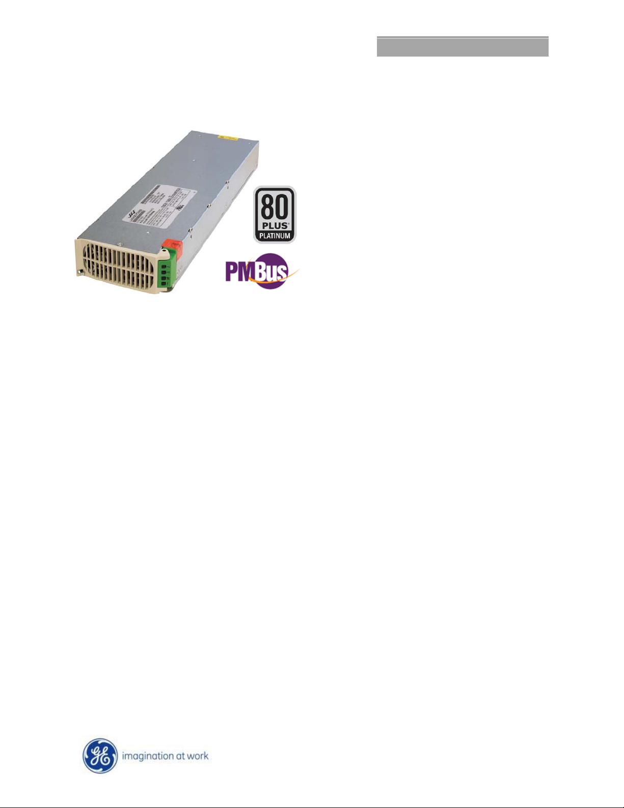
CP2725AC54TE Compact Power Line High Efficiency Rectifier
100-120/200-277VAC input; Default Outputs: ±54VDC @ 2725W, 5VDC @ 4W
RoHS Compliant
Applications
48V
Routers/Switches
VoIP/Soft Switches
LAN/WAN/MAN applications
File servers
Indoor wireless
Telecommunications equipment
Enterprise Networks
SAN/NAS/iSCSI applications
distributed power architectures
DC
Features
Efficiency 96.2%
Compact 1RU form factor with 30 W/in
Constant power from 52 – 58V
2725W from nominal 200 – 277V
1200W from nominal 100 – 120V
Output voltage programmable from 42V – 58V
2
PMBus compliant dual I
Isolated +5V Aux, signals and I
Power factor correction (meets EN/IEC 61000-3-2 and
EN 60555-2 requirements)
Output overvoltage and overload protection
AC Input overvoltage and undervoltage protection
Over-temperature warning and protection
Redundant, parallel operation with active load sharing
Remote ON/OFF
Internally controlled Variable-speed fan
Hot insertion/removal (hot plug)
Four front panel LED indicators
UL* Recognized to UL60950-1, CAN/ CSA
60950-1, and VDE
CE mark meets 2006/95/EC directive
RoHS 6 compliant
C and RS485 serial busses
‡
0805-1 Licensed to IEC60950-1
3
density
DC
AC
AC
2
C communications
†
C22.2 No.
§
DC
Description
The CP2725AC54TE Rectifier provides significant efficiency improvements in the Compact Power Line platform of Rectifiers. Highdensity front-to-back airflow is designed for minimal space utilization and is highly expandable for future growth. The wide-input
standard product is designed to be deployed internationally. It is configured with both RS485 and dual-redundant I
communications busses that allow it to be used in a broad range of applications. These signals and the 5V auxiliary supply are
isolated from the main output and frame ground. Feature set flexibility makes this rectifier an excellent choice for applications
requiring modular AC to - 48V
intermediate voltages, such as in distributed power.
DC
*
UL is a registered trademark of Underwriters Laboratories, Inc.
†
CSA is a registered trademark of Canadian Standards Association.
‡
VDE is a trademark of Verband Deutscher Elektrotechniker e.V.
§ This product is intended for integration into end-user equipment. All CE marking procedures of end-user equipment should be followed. (The CE mark is placed on selected products.)
** ISO is a registered trademark of the International Organization of Standards
+
The PMBus name and logo are registered trademarks of the System Management Interface Forum (SMIF)
January 30, 2014 ©2013 General Electric Company. All rights reserved.
2
C
Page 2
GE
Data Sheet
CP2725AC54TE CPL High Efficiency Rectifier
100-120/200-277VAC input; Default Outputs: ±54V
Absolute Maximum Ratings
Stresses in excess of the absolute maximum ratings can cause permanent damage to the device. These are absolute stress ratings
only, functional operation of the device is not implied at these or any other conditions in excess of those given in the operations
sections of the data sheet. Exposure to absolute maximum ratings for extended periods can adversely affect the device reliability.
Parameter Symbol Min Max Unit
Input Voltage: Continuous VIN 0 300 VAC
Operating Ambient Temperature TA -10 751 °C
Storage Temperature Tstg -40 85 °C
I/O Isolation voltage to Frame (100% factory Hi-Pot tested) 1500 VAC
Electrical Specifications
Unless otherwise indicated, specifications apply over all operating input voltage, Vo=54VDC, resistive load, and temperature
conditions.
INPUT
Parameter Symbol Min Typ Max Unit
Startup Input Voltage
Low-line Operation
High-line Operation
Operating Voltage Range
Low-line Configuration
High-line Configuration
Input Voltage Swell (no damage) 305
Input Frequency F
Input Current; at 110VAC
at 240V
Inrush Transient (at 25°C, excluding X-Capacitor charging) I
Idle Power (at 220VAC) 54V OFF
54V ON @ Io=0
Input Leakage Current (265VAC, 60Hz) I
Power Factor (50 – 100% load) PF 0.96 0.995
Efficiency2 (30 – 80% of FL, 240VAC @ 25C)
Holdup time (output allowed to decay down to 40VDC)
For loads below 1200W
Ride thru (tested at 115V @ 230V. (Complies to CISPR24) T 1/2 1 cycle
Power Fail Warning3 (main output allowed to decay to 40VDC) PFW 3 5 ms
Isolation (per EN60950) (consult factory for testing to this requirement)
Input-Chassis/Signals
Input - Output
AC
@ 2725W, 5V
DC
V
IN
V
IN
IN
I
IN
IN
P
IN
IN
T
V
185
94.5 96.2 %
1500
3000
DC
90
47 66 Hz
25 30 APK
2.5 3.5 mA
@ 4W
100 – 120
200 - 277
11.9
13.1
8.2
16
20
30
90
185
140
300
A
W
ms
V
V
VAC
V
AC
AC
AC
AC
1
Derated above 50C at 2.5%/C
2
See efficiency curve in the Characteristics Curves section.
3
Internal protection circuits may override the PFW signal and may trigger an immediate shutdown.
January 30, 2014 ©2013 General Electric Company. All rights reserved. Page 2
Page 3
GE
Data Sheet
CP2725AC54TE CPL High Efficiency Rectifier
100-120/200-277VAC input; Default Outputs: ±54V
Electrical Specifications (continued)
54VDC MAIN OUTPUT
Parameter Symbol Min Typ Max Unit
Output Power @ low line input 100 – 120VAC
@ high line input 200 – 277V
@ nominal 277Vac and T
Default Set point
Overall regulation (load, temperature, aging) 0 - 45C LOAD > 2.5A
> 45C
Output Voltage Set Range - analog margining
- Set either by I
2
C or RS485
Output Current - @ 1200W (100 – 120Vac), 54V/52V
@ 2725W (200 – 240V
@ 2000W ( > 277V
@ Tamb > 45C), 54V/52V
AC
Current Share ( > 50% FL) -5 5 %FL
Proportional Current Share between different rectifiers ( > 50% FL) <7 %FL
Output Ripple ( 20MHz bandwidth, load > 1A)
RMS (5Hz to 20MHz)
Peak-to-Peak (5Hz to 20MHz)
Psophometric Noise
External Bulk Load Capacitance C
Turn-On (monotonic turn-ON from 30 – 100% of Vnom above 5C)
Delay
Rise Time – PMBus mode
Rise Time - RS-485 mode
Output Overshoot
Load Step Response ( I
O,START
I
285
V, V
AC
V, VAC 285
AC
AC
Response Time
Overload - Power limit @ high line down to 52V
Power limit @ low line down to 52V
High line current limit if V
High line current limit if V
Low line current limit
Output shutdown (commences as voltage decays below this level)
System power up Upon insertion the power supply will delay an overload shutdown
Overvoltage - 200ms delayed shutdown
Immediate shutdown
Latched shutdown Three restart attempts are implemented within a 1 minute window
Over-temperature warning (prior to commencement of shutdown)
Shutdown (below the max device rating being protected)
Restart attempt Hysteresis (below shutdown level)
Isolation Output-Chassis (Standard, non-POE compliant)
Output-Chassis/Signals (POE compliant per IEEE802.3)
amb
), 54V/52V
AC
6
> 2.5A )
> 41.5V
out
< 41.5V
out
AC
> 45C
DC
DC
DC
DC
@ 2725W, 5V
DC
DC
@ 4W
1200
W
2725
W
2000
54 V
V
OUT
-2
44
42
-1
1
I
Out
1
1
+1
+2
58
58
25/23
50.5/52.4
37/38.4
V
OUT
OUT
T
V
OUT
I
OUT
V
OUT
V
OUT
T
P
OUT
P
OUT
I
OUT
V
OUT
0 5,000
5
100
5
2.0
3.2
2
2725
1200
53
36
26
100
300
9
2
50
39
5
mV
4
mV
mV
for 20 seconds allowing for the insertion and startup of multiple
modules within a system.
V
OUT
> 65
< 65
prior to a latched shutdown.
5
T
20
10
V
500
2250
DC
DC
%
V
DC
A
DC
F
s
ms
s
%
%FL
V
DC
VDC
ms
W
DC
W
DC
A
DC
A
DC
A
DC
V
DC
V
DC
C
V
DC
VDC
rms
p-p
rms
4
500mVp-p max above 280V
5
Complies with ANSI TI.523-2001 section 4.9.2 emissions max limit of 20mV flat unweighted wideband noise limits
6
Below -5°C, the rise time is approximately 5 minutes to protect the bulk capacitors.
input or above 56Vdc output;
AC
January 30, 2014 ©2013 General Electric Company. All rights reserved. Page 3
Page 4
GE
Data Sheet
CP2725AC54TE CPL High Efficiency Rectifier
100-120/200-277VAC input; Default Outputs: ±54V
5V
Auxiliary output
DC
Parameter Symbol Min Typ Max Unit
Output Voltage Setpoint V
Overall Regulation -107 +5 %
Output Current 0.005 0.75 A
Ripple and Noise (20mHz bandwidth) 50 100 mV
Over-voltage Clamp 7 VDC
Over-current Limit 110 175 %FL
Isolation from the main output STD / POE compliant
Isolation from frame ground
General Specifications
@ 2725W, 5V
DC
5 VDC
OUT
500 / 2250
50
DC
@ 4W
p-p
Vdc
Vdc
Parameter Min Typ Max
Reliability 450,000 Hours
Units
Notes
Full load, 25C ; MTBF per SR232 Reliability protection for
electronic equipment, issue 2, method I, case III,
Service Life 10 Years Full load, excluding fans
Unpacked Weight 2.18/4.8 Kgs/Lbs
Packed Weight 2.45/5.4 Kgs/Lbs
Heat Dissipation 100 Watts or 341 BTUs @ 80% load, 153 Watts or 522 BTUs @ 100% load
Feature Specifications
Unless otherwise indicated, specifications apply over all operating input voltage, resistive load, and temperature conditions. Signals are referenced
to Logic_GRD unless noted otherwise. Fault, PFW, OTW, SMBAlert#, and Power capacity need to be pulled HI through external pull-up resistors. See
Feature Descriptions for additional information.
Parameter Symbol Min Typ Max Unit
Enable (should be connected to Logic_GRD) 54V output OFF V
54V output ON V
Margining (through adjusting Vcontrol)
Voltage control range V
Programmed output voltage range V
Voltage adjustment resolution (8-bit A/D) V
Output configured to 54VDC V
Output configured to 44VDC V
ON/OFF [short pin controls 54V
output - ] referenced to VOUT( - )
DC
54V output OFF V
54V output ON V
Module Present [Resistor connected to Logic_GRD internally]
Write protect enabled V 1
Write protect disabled V
Over Temperature Warning (OTW) Logic HI (temperature normal) V 0.7V
Sink current I
Logic LO (temperature is too high) V
Fault Logic HI (No fault is present) V 0.7V
Sink current I
Logic LO (Fault is present) V
SMBAlert# (Alert#_0, Alert#_1) Logic HI (No Alert - normal) V 0.7V
Sink current I
Logic LO (Alert is set) V
1.4
OUT
OUT
0 3.3 VDC
control
OUT
control
3.0 3. 3 VDC
control
0 0.1 VDC
control
1.4
control
control
0
44 58 VDC
42 58 VDC
3.3 mVDC
0
500
0
DD
0
DD
0
DD
0
5 V
0.8 VDC
5 VDC
0.8 VDC
5 VDC
0.8 VDC
12 V
5 mA
0.4 VDC
12 V
5 mA
0.4 VDC
12 V
5 mA
0.4 VDC
DC
DC
DC
DC
7
Within ±5% when load is < 0.5A
January 30, 2014 ©2013 General Electric Company. All rights reserved. Page 4
Page 5
GE
Data Sheet
CP2725AC54TE CPL High Efficiency Rectifier
100-120/200-277VAC input; Default Outputs: ±54V
Feature Specifications (continued)
Parameter Symbol Min Typ Max Unit
Power Capacity Logic HI V 0.7V
Logic LO V
Reset Logic HI
Logic LO V
Protocol select Logic HI - Analog/PMBus™ mode
Logic – intermediate – RS485 mode V
Logic LO – DSP reprogram mode VIL 0
Digital Interface Specifications
Parameter Conditions Symbol Min Typ Max Unit
PMBus Signal Interface Characteristics
Input Logic High Voltage (CLK, DATA) V 1.5 3.6 VDC
Input Logic Low Voltage (CLK, DATA) V 0 0.8 VDC
Input high sourced current (CLK, DATA) I 0 10 A
Output Low sink Voltage (CLK, DATA, SMBALERT#) I
Output Low sink current (CLK, DATA, SMBALERT#) I 3.5 mA
Output High open drain leakage current (CLK,DATA,
SMBALERT#)
PMBus Operating frequency range Slave Mode FPMB 10 400 kHz
Measurement System Characteristics
Clock stretching T
I
measurement range Direct I
OUT
I
measurement accuracy 25°C I
OUT
V
measurement range Direct V
OUT
V
measurement accuracy9 V
OUT
Temp measurement range
Temp measurement accuracy10 Temp
VIN measurement range Direct V
VIN measurement accuracy V
PIN measurement range Direct P
PIN measurement accuracy11 P
Fan Speed measurement range Direct 0 30k RPM
Fan Speed measurement accuracy -10 10 %
Fan speed control range Direct 0 100 %
Device Addressing
Unit address [reference: V
OUT
( - )]
Shelf address [reference: V
OUT
( - )]
8
Load levels higher than 50A will be read as 50A.
9
Above 2.5A of load current
10
Temperature accuracy reduces non-linearly with decreasing temperature
11
Below 100W input power measurement accuracy reduces significantly
=3.5mA V 0.4 VDC
OUT
V
=3.6V I
OUT
Direct
Module 1 V
Module 2 V
Module 3 V
Module 4 V
Shelf 1 V
Shelf 2 V
Shelf 3 V
Shelf 4 V
Shelf 5 V
Shelf 6 V
Shelf 7 V
Shelf 8 V
@ 2725W, 5V
DC
V
V
2.7
IH
II
25 ms
stretch
rng
out(acc)
0 70 VDC
out(rng)
out(acc)
Temp
0 150
(rng)
(acc)
0 320 VAC
in(rng)
in(acc)
0 3000 W
in(rng)
in(acc)
unitadr
unitadr
unitadr
unitadr
shelfadr
shelfadr
shelfadr
shelfadr
shelfadr
shelfadr
shelfadr
shelfadr
@ 4W
DC
12 V
0.4 VDC
12 V
0.4 VDC
3.5 V
0.7V
DD
0
DD
0
1.0 2.65 VDC
0.4 VDC
0 10 A
0 508 A
-2.5 +2.5 % of FL
-1 +1 %
-5 +5 %
-1.5 +1.5 %
-3.5 +3.5 %
2.3 2.477 3.3 VDC
1.6 1.925 2.2 VDC
0.9 1.243 1.5 VDC
0 0.654 0.8 VDC
3.0 3.3 3.45 VDC
2.7 2.86 2.97 VDC
2.18 2.4 2.56 VDC
1.73 1.96 2.14 VDC
1.29 1.50 1.70 VDC
0.84 1.10 1.25 VDC
0.30 0.60 0.80 VDC
0 0.01 0.25 VDC
DC
DC
DC
C
DC
in
January 30, 2014 ©2013 General Electric Company. All rights reserved. Page 5
Page 6
GE
CP2725AC54TE CPL High Efficiency Rectifier
100-120/200-277VAC input; Default Outputs: ±54V
Environmental Specifications
@ 2725W, 5V
DC
DC
@ 4W
Data Sheet
Parameter Min Typ
Ambient Temperature -4012 5513 °C Air inlet from sea level to 5,000 feet.
Storage Temperature -40 85 °C
Operating Altitude 1524/5000 m / ft
Non-operating Altitude 8200/30k m / ft
Power Derating with Temperature 2.0 %/°C
Power Derating with Altitude 2.0
Acoustic noise 55 dbA Full load
Over Temperature Protection
Humidity
Operating
Storage
Shock and Vibration acceleration 6 Grms
Earthquake Rating 4
125/110
5
5
Max
95
95
Units
55°C to 75C
C/305 m
C/1000 ft
°C
%
%
Zone
Above 1524/5000 m/ft; 3962/13000 m/ft
max
Shutdown / restart [internally measured
points]
Relative humidity, non-condensing
NEBS GR-63-CORE, Level 3, 20 -2000Hz, min
30 minutes
NEBS GR-63-CORE, all floors, Seismic Zone 4
Designed and tested to meet NEBS
specifications.
Notes
14
EMC
Parameter Criteria Standard
AC input
AC Input
Immunity
Enclosure
immunity
Conducted emissions EN55022, FCC Docket 20780 part 15, subpart J
Radiated emissions EN55022 A 30 – 10000MHz
Line sags and
interruptions
Lightning surge EN61000-4-5, Level 4, 1.2/50µs – error free A 4kV, common mode
Fast transients EN61000-4-4, Level 3 B 5/50ns, 2kV (common mode)
Conducted RF fields EN61000-4-6, Level 3 A 130dBµV, 0.15-80MHz, 80% AM
Radiated RF fields EN61000-4-3, Level 3 A 10V/m, 80-1000MHz, 80% AM
ENV 50140 A
ESD EN61000-4-2, Level 3 B 6kV contact, 8kV air
EN61000-3-2
Meets Telcordia GR1089-CORE by a 3dB margin
EN61000-4-11 B -30%, 10ms
Output will stay above 40VDC @ full load 25% line sag for 2 seconds
Sag must be higher than 80Vrms. 1 cycle interruption
ANSI C62.41 - damage free A3 6kV, common & differential
12
Designed to start and work at an ambient as low as -40°C, but may not meet operational limits until above -5°C
13
Output power is derated to 2kW for temperatures higher than 45C and input voltages higher than 285VAC.
14
The maximum operational ambient is reduced in Europe in order to meet certain power cord maximum ratings of 70C. The maximum
operational ambient where 70C rated power cords are utilized is reduced to 60C until testing demonstrates that a higher level is acceptable.
Level
A 0.15 – 30MHz
0 – 2 KHz
B -60%, 100ms
B -100%, 5sec
A 2kV, differential mode
Test
January 30, 2014 ©2013 General Electric Company. All rights reserved. Page 6
Page 7

GE
CP2725AC54TE CPL High Efficiency Rectifier
100-120/200-277VAC input; Default Outputs: ±54V
Characteristic Curves
The following figures provide typical characteristics for the
CP2725AC54TE rectifier
@ 2725W, 5V
DC
and 25oC.
DC
Data Sheet
@ 4W
98
96
94
92
90
88
86
84
EFFICIENCY, (%)
82
80
0 5 10 15 20 25 30 35 40 45 50 55
Vin=110V
OUTPUT CURRENT, IO (A) OUTPUT CURRENT
Vin=240V
Figure 1. Rectifier Efficiency versus Output Current.
60
55
50
45
VOLTAGE
40
35
OUTPUT
30
15 20 25 30
OUTPUT CURRENT
Figure 3. 54V
shutdown profile at V
output: Power limit, Current limit and
DC
= 90VAC.
IN
60
55
50
45
VOLTAGE
40
35
OUTPUT
30
40 45 50 55
Figure 2. 54V
shutdown profile at V
3000
2800
2600
2400
2200
2000
1800
1600
1400
OUTPUT POWER
1200
1000
120 140 160 180 200
Figure 4. 54V
input voltage.
output: Power limit, Current limit and
DC
Equation for derating zone
= 185VAC.
IN
y = 55.015Vin - 6991.6
tolerance: ±5%
INPUT VOLTAGE
output: Output power derating based on
DC
VOLTAGE
(V) (200mV/div)
O
V
OUTPUT
TIME, t (10ms /div) TIME, t (10ms/div)
Figure 5. 54VDC output ripple and noise, full load,
V
= 185VAC.
IN
(V) (20mV/div)
O
OUTPUT VOLTAGE
V
Figure 6. 5V
V
= 185VAC.
IN
output ripple and noise, all full load,
DC
January 30, 2014 ©2013 General Electric Company. All rights reserved. Page 7
Page 8

GE
OUTPUT
CIURRENT
OUUT
PUT VOLTAGE
OUTPUT
CIURRENT
OUUT
PUT VOLTAGE
-
CP2725AC54TE CPL High Efficiency Rectifier
100-120/200-277VAC input; Default Outputs: ±54V
Characteristic Curves (continued)
The following figures provide typical characteristics for the
CP2725AC54TE rectifier
@ 2725W, 5V
DC
and 25oC.
DC
@ 4W
Data Sheet
(V) (1V/div)
O
(V) (20A/div) V
O
I
TIME, t (20ms/div) OUTPUT CURRENT, IO (A)
Figure 7. Transient response 54VDC load step 2.5 – 27.2A,
V
= 185VAC.
IN
VOLTAGE
(V) (200mV/div)
O
V
OUTPUT
Figure 9. 54V
2
I
C mode.
soft start, no-load & full load, VIN=185V
DC
TIME, t (50ms/div) TIME, t (2s/div)
(V) (1V/div)
O
(V) (20A/div) V
O
I
Figure 8. Transient response 54V
V
= 185VAC.
IN
(V) (10V/div)
O
V
OUTPUT VOLTAGE
load step 27.2 – 2.5A,
DC
AC
Figure 10. 54V
soft start, full load, V
DC
= 185VAC -
IN
RS485 mode.
(V) (10V/div)
O
(V) (100V/div) V
IN
V
INPUT VOLTAGE OUUTPUT VOLTAGE
TIME, t (10ms/div) TIME, t (10ms/div)
Figure 11. Ride through missing 1 cycle, full load,
V
= 230VAC.
IN
(V) (10V/div)
O
(V) (5V/div) V
PFW
PFW SIGNAL OUUTPUT VOLTAGE
V
Figure 12. PFW alarmed 19.6ms prior to Vo < 40V,
output load: 38A, V
= 185VAC.
IN
January 30, 2014 ©2013 General Electric Company. All rights reserved. Page 8
Page 9

GE
1
5
u
tput Setpoint (
V
c
p
rog
r
CP2725AC54TE CPL High Efficiency Rectifier
100-120/200-277VAC input; Default Outputs: ±54V
Control and Status
The Rectifier provides three means for monitor/control: analog,
PMBus™, or the GE Galaxy-based RS485 protocol.
Details of analog control and the PMBus™ based protocol are
provided in this data sheet. GE will provide separate
application notes on the Galaxy RS485 based protocol for
users to interface to the rectifier. Contact your local GE
representative for details.
Signal Reference
Unless otherwise noted, all signals are referenced to
Logic_GRD. See the Signal Definitions Table at the end of this
document for further description of all the signals.
Logic_GRD is isolated from the main output of the power
supply for PMBus communications. Communications and the
5V standby output are not connected to main power return
(Vout(-)) and can be tied to the system digital ground point
selected by the user. (Note that RS485 communications is
referenced to Vout(-), main power return of the power supply).
Logic_GRD is capacitively coupled to Frame_GRD inside the
power supply. The maximum voltage differential between
Logic_GRD and Frame_GRD should be less than 100V
.
DC
Control Signals
Enable: Controls the main 54VDC output when either analog
control or PMBus protocols are selected, as configured by the
Protocol pin. This pin must be pulled low to turn ON the
rectifier. The rectifier will turn OFF if either the Enable or the
ON/OFF pin is released. This signal is referenced to Logic_GRD.
In RS485 mode this pin is ignored.
ON/OFF: This is a shorter pin utilized for hot-plug applications
to ensure that the rectifier turns OFF before the power pins are
disengaged. It also ensures that the rectifier turns ON only
after the power pins have been engaged. Must be connected
to V_OUT ( - ) for the rectifier to be ON.
Margining: The 54V
58V
by a control voltage on the Margin pin. This control
DC
voltage can be generated either from an external voltage
source, or by forming a voltage divider between 3.3V and
Logic_GRD, as shown in Fig. 13. The power supply includes the
high side pull-up 10k resistor to 3.3V
between the margin pin and Logic_GRD will complete the
divider.
An open circuit, or a voltage level > 3.0V
main output to the factory default setting of 54V
Hardware margining is only effective until software
commanded output voltage changes are not executed.
Software commanded output voltage settings permanently
override the hardware margin setting until power to the
internal controller is interrupted, for example if input power or
bias power is recycled.
The controller always restarts into its default configuration,
programmed to set the output as instructed by the margin pin.
Subsequent software commanded settings permanently
override the margin pin. Adding a resistor between margin and
Vout(-) is an ideal way of changing the factory set point of the
rectifier to whatever voltage level is desired by the user.
output can be adjusted between 44 –
DC
. Connecting a resistor
DC
, on this pin sets the
DC
.
DC
@ 2725W, 5V
DC
-58
-54
)
-46
d
-44
O
0
Figure 13. Diagram showing how output can be margined
using Vcontrol adjustment.
Module Present Signal: This signal has dual functionality. It
can be used to alert the system when a rectifier is inserted. A
500 resistor is present in series between this signal and
Logic_GRD. An external pull-up should not raise the voltage on
the pin above 0.25V
, the write_protect feature of the EEPROM is enabled.
1V
DC
8V_INT: Single wire connection between modules, Provides
bias to the DSP of an unpowered module.
Reset: This is a PCA9541 multiplexer function utilized during
PMBus communications. If momentarily grounded (Logic_GRD),
the multiplexer would reset itself.
Protocol: Establishes the communications mode of the
rectifier, between analog/PMBus and RS485 modes. For RS485,
connect a 10k pull-down resistor from this pin to V_OUT( - ).
For analog/PMBus leave the pin open. Do not tie this signal pin
to V_OUT( - ) because that connection configures the internal
DSP into a reprogrammed state.
Unit Address: Each module has an internal 10k resistor
pulled up between unit_address and 3.3V
between unit_address and Vout(-) sets the appropriate unit
address.
Shelf Address: By applying the required voltage between the
shelf address pin and Vout(-), up to 8 different shelves and so
up to 32 different modules can be addressed using either the
PMBus or GE Galaxy based RS485 protocol.
PMBus addressing is limited to a maximum of 8 modules and
so the software decodes the shelf address setting into either
shelf 0 or shelf 1 in PMBus applications. If more than two
shelves are paralleled, the user must separate the I
that address conflicts do not occur.
Maximum voltage 3.45 2.97 2.56 2.14
Nominal voltage 3.30 2.86 2.4 1.96
Minimum voltage 3.00 2.60 2.18 1.73
Address bit- A2 0 1 0 1
Maximum voltage 1.70 1.25 0.80 0.25
Nominal voltage 1.50 1.10 0.60 0.01
Minimum voltage 1.29 0.84 0.30 0
Address bit- A2 0 1 0 1
0.1
Vcontrol (Vdc )
DC
Shelf_address
Shelf_address
Preliminary Data Sheet
@ 4W
DC
3.3Vdc
10k
Vcon trol
am
Inside
module
3.3
3.0
. When the voltage on this pin exceeds
. A resistor
DC
2 3 4
6 7 8
R
2
C lines so
January 30, 2014 ©2013 General Electric Company. All rights reserved. Page 9
Page 10

GE
CP2725AC54TE CPL High Efficiency Rectifier
100-120/200-277VAC input; Default Outputs: ±54V
Status Signals
Power Capacity: A HI on this pin indicates that the rectifier
delivers high line rated output power; a LO indicates that the
rectifier is connected to low line configured for 1200W
operation.
Power Fail Warning: This signal is HI when the main output is
being delivered and goes LO for the duration listed in this data
sheet prior to the output decaying below the listed voltage
level.
Fault: This signal goes LO for any failure that requires rectifier
replacement. These faults may be due to:
Fan failure
Over-temperature warning
Over-temperature shutdown
Over-voltage shutdown
Internal Rectifier Fault
Digital Feature Descriptions
PMBus™ compliance: The power supply is fully compliant to
the Power Management Bus (PMBus™) rev1.2 requirements
with the following exceptions:
The power supply continuously updates its STATUS and ALARM
registers to the latest state in order to capture the ‘present’
state of the power supply. There are a number of indicators,
such as those indicating a communications fault (PEC error,
data error) that do not get cleared until specifically instructed
by the host controller sending a clear_faults command. A ‘bit’
indicator notifies the user if the STATUS and ALARM registers
changed since the last ‘read’ by the host controller.
For example, if a voltage surge causes a momentary shutdown
for over voltage the power supply will automatically restart if
the ‘auto_restart’ feature is invoked. During the momentary
shutdown the power supply issues an Alert# indicating to the
system controller that a status change has occurred. If the
system controller reads back the STATUS and ALARM registers
while the power supply is shut down it will get the correct fault
condition. However, inquiry of the state of the power supply
after the restart event would indicate that the power supply is
functioning correctly. The STATUS and ALARM indicators did
not freeze at the original shutdown state and so the reason for
the original Alert# is erased. The restart ‘bit’ would be set to
indicate that an event has occurred.
The power supply also clears the STATUS and ALARM registers
after a successful read back of the information in these
registers, with the exception of communications error alarms.
This automated process improves communications efficiency
since the host controller does not have to issue another
clear_faults command to clear these registers.
2
Dual, redundant buses: Two independent I
true communications bus redundancy and allow two
independent controllers to sequentially control the power
supply. For example, a short or an open connection in one of
2
C lines does not affect communications capability on the
the I
2
other I
C line. Failure of a ‘master’ controller does not affect the
power supplies and the second ‘master’ can take over control
at any time.
C lines provide
@ 2725W, 5V
DC
Using the PCA9541 multiplexer: Transition between the two
2
I
C lines is provided by the industry standard PCA9541 I2C
master selector multiplexer. Option 01 of the device code is
supplied which, upon start-up, connects channel 0 to the
power supply. In this fashion applications using only a single
2
C line can immediately start talking across the bus without
I
first requiring to reconfigure the multiplexer.
Figure 14. Diagram showing conceptual representation
of the dual I
Control can be taken over at any time by a specific ‘master’
even during data transmission to the other ‘master’. The
‘master’ needs to be able to handle incomplete transmissions
in the multi-master environment in case switching should
commence in the middle of data transmission.
Master/Slave: The ‘host controller’ is always the MASTER.
Power supplies are always SLAVES. SLAVES cannot initiate
communications or toggle the Clock. SLAVES also must
respond expeditiously at the command of the MASTER as
required by the clock pulses generated by the MASTER.
Clock stretching: The ‘slave’ µController inside the power
supply may initiate clock stretching if it is busy and it desires to
delay the initiation of any further communications. During the
clock stretch the ‘slave’ may keep the clock LO until it is ready
to receive further instructions from the host controller. The
maximum clock stretch interval is 25ms.
The host controller needs to recognize this clock stretching,
and refrain from issuing the next clock signal, until the clock
line is released, or it needs to delay the next clock pulse
beyond the clock stretch interval of the power supply.
Note that clock stretching can only be performed after
completion of transmission of the 9
being the START command.
Figure 14. Example waveforms showing clock stretching.
Communications speed: Both 100kHz and 400kHz clock rates
are supported. The power supplies default to the 100kHz clock
rate.
DC
2
C bus system.
Data Sheet
@ 4W
th
ACK bit, the exception
Clock
Stretch
January 30, 2014 ©2013 General Electric Company. All rights reserved. Page 10
Page 11

GE
CP2725AC54TE CPL High Efficiency Rectifier
100-120/200-277VAC input; Default Outputs: ±54V
Packet Error Checking: The power supply will not respond to
commands without the trailing PEC. The integrity of
communications is compromised if packet error correction is
not employed. There are many functional features, including
turning OFF the main output, that require validation to ensure
that the correct command is executed.
PEC is a CRC-8 error-checking byte, based on the polynomial
8
+ x2 + x + 1, in compliance with PMBus™
C(x) = x
requirements. The calculation is based in all message bytes,
including the originating write address and command bytes
preceding read instructions. The PEC is appended to the
message by the device that supplied the last byte.
SMBusAlert#: The power supply can issue SMBAlert# driven
from either its internal micro controller (µC) or from the
PCA9541 I
of the internal µC funnels through the PCA9541 master
selector that buffers the SMBAlert# signal and splits the signal
to the two SMBAlert# signal pins exiting the power supply. In
addition, the PCA9541 signals its own SMBAlert# request to
either of the two SMBAlert# signals when required.
Non-supported commands: Non supported commands are
flagged by setting the appropriate STATUS bit and issuing an
SMBAlert# to the ‘host’ controller.
Data out-of-range: The power supply validates data settings
and sets the data out-of-range bit and SMBAlert# if the data is
not within acceptable range.
SMBAlert# triggered by the µC: The µC driven SMBAlert#
signal informs the ‘master/host’ controller that either a STATE
or ALARM change has occurred. Normally this signal is HI. The
signal will change to its LO level if the power supply has
changed states and the signal will be latched LO until the
power supply receives a ‘clear’ instruction as outlined below. If
the alarm state is still present after the ‘clear_faults’ command
has been received, then the signal will revert back into its LO
level again and will latch until a subsequent ‘clear’ signal is
received from the host controller.
The signal will be triggered for any state change, including the
following conditions;
VIN under or over voltage
Vout under or over voltage
IOUT over current
Over Temperature warning or fault
Fan Failure
Communication error
PEC error
Invalid command
Internal faults
The power supply will clear the SMBusAlert# signal (release the
signal to its HI state) upon the following events:
Completion of a ‘read_status’ instruction
Receiving a CLEAR_FAULTS command
The main output recycled (turned OFF and then ON) via
The main output recycled (turned OFF and then ON) by the
SMBAlert# triggered by the PCA9541: If clearing the Alert#
signal via the clear_faults or read back fails, then reading back
2
C bus master selector. That is, the SMBAlert# signal
the ENABLE signal pin
OPERATION command
@ 2725W, 5V
DC
the Alert# status of the PCA9541 will be necessary followed by
clearing of the PCA9541 Alert#.
The PCA9541 can issue an Alert# even when single bus
operation is selected where the bus master selector has not
been used or addressed. This may occur because the default
state of the PCA9541/01 integrated circuit issues Alert# to both
2
i
C lines for all possible transitioning states of the device. For
example, a RESET caused by a glitch would cause the Alert# to
be active.
If the PCA9541 is not going to be used in a specific application
(such as when only a single I
that interrupts from the PCA9541 are de-activated by the host
controller. To de-activate the interrupt registers the PCA9541
the ‘master’ needs to address the PCA9541 in the ‘write’ mode,
the interrupt enable (IE) register needs to be accessed and the
interrupt masks have to be set to HI ‘1’. (Note: do not mask bit
0 which transmits Alert# from the power supply). This
command setting the interrupt enable register of the PCA9541
is shown below;
Start
1 7 6 5 4 3 2 1 0 1
S 1 1 1 0 A2 A1 A0 0 A
Command Code
There are two independent interrupt enable (IE) registers, one
for each controller channel (I
register of each channel needs to be configured
independently. That is, channel I
register of I
This command has to be initiated to the PC9541 only once
after application of power to the device. However, every time a
restart occurs the PCA9541 has to be reconfigured since its
default state is to issue Alert# for changes to its internal status.
If the application did not configure the interrupt enable register
the Alert# line can be cleared (de-activated), if it has been
activated by the PCA9541, by reading back the data from the
interrupt status registers (Istat).
Refer to the PCA9541 data sheet for further information on
how to communicate to the PCA9541 multiplexer.
Please note that the PCA9541 does not support Packet Error
Checking (PEC).
Re-initialization: The I
no activity is detected on the bus for 5 seconds. Reinitialization is designed to guarantee that the I
does not hang up the bus. Although this rate is longer than the
timing requirements specified in the SMBus specification, it
had to be extended in order to ensure that a re-initialization
would not occur under normal transmission rates. During the
few µseconds required to accomplish re-initialization the I
µController may not recognize a command sent to it. (i.e. a
start condition).
Global broadcast: This is a powerful command because it can
instruct all power supplies to respond simultaneously in one
command. But it does have a serious disadvantage. Only a
single power supply needs to pull down the ninth acknowledge
Data Sheet
@ 4W
DC
2
C line is utilized), it is imperative
Unit Address ACK
8 1 8
0x00 A 0x0E P
2
C-1 or vise-versa.
ACK IE Register
2
C-0 and I2C-1). The interrupt
2
C-0 cannot configure the IE
2
C code is programmed to re-initialize if
2
Stop
C µController
2
C
January 30, 2014 ©2013 General Electric Company. All rights reserved. Page 11
Page 12

GE
R
CP2725AC54TE CPL High Efficiency Rectifier
100-120/200-277VAC input; Default Outputs: ±54V
bit. To be certain that each power supply responded to the
global instruction, a READ instruction should be executed to
each power supply to verify that the command properly
executed. The GLOBAL BROADCAST command should only be
executed for write instructions to slave devices.
Note: The PCA9541 i2c master selector does not respond to the
GLOBAL BROADCAST command.
Read back delay: The power supply issues the SMBAlert #
notification as soon as the first state change occurred. During
an event a number of different states can be transitioned to
before the final event occurs. If a read back is implemented
rapidly by the host a successive SMBAlert# could be triggered
by the transitioning state of the power supply. In order to avoid
successive SMBAlert# s and read back and also to avoid
reading a transitioning state, it is prudent to wait more than 2
seconds after the receipt of an SMBAlert# before executing a
read back. This delay will ensure that only the final state of the
power supply is captured.
Successive read backs: Successive read backs to the power
supply should not be attempted at intervals faster than every
one second. This time interval is sufficient for the internal
processors to update their data base so that successive reads
provide fresh data.
Device ID: Address bits A2, A1, A0 set the specific address of
the power supply. The least significant bit x (LSB) of the address
byte configures write [0] or read [1] events. In a write
command the system instructs the power supply. In a read
command information is being accessed from the power
supply.
Address Bit
7 6 5 4 3 2 1 0
PCA9541 1 1 1 0 A2 A1 A0 R/W
Micro controller 1 0 0 0 A2 A1 A0 R/W
External EEPROM 1 0 1 0 A2 A1 A0 R/W
Global Broadcast 0 0 0 0 0 0 0 0
MSB LSB
The Global Broadcast instruction executes a simultaneous
write instruction to all power supplies. A read instruction
cannot be accessed globally. The three programmable address
bits are the same for all I
2
C accessible devices within the
power supply.
PMBusTM Commands
Standard instruction: Up to two bytes of data may follow an
instruction depending on the required data content. Analog
data is always transmitted as LSB followed by MSB. PEC is
mandatory and includes the address and data fields.
1 8 1 8 1
S Slave address Wr A Command Code A
8 1 8 1 8 1 1
Low data byte A High data byte A PEC A P
Master to Slave Slave to Master
SMBUS annotations; S – Start , Wr – Write, Sr – re-Start, Rd – Read,
A – Acknowledge, NA – not-acknowledged, P – Stop
Direct mode data format: The Direct Mode data format is
supported, where y = [ mX + b ] x 10
R
. In the equation, y is the
@ 2725W, 5V
DC
data value from the controller and x is the ‘real’ value either
being set or returned.
For example, to set the output voltage to 50.45V
desired set point by the m constant, 50.45 x 400 = 20,180.
Convert this binary number to its hex equivalent: 20,180b =
0x4ED4. The result is sent LSB=0xD4 first, then MSB=0x4E.
The constants are
FUNCTION
Output voltage
Output voltage shutdown
Output Current read 5 0 0
Temperature read 1 0 0
Input Voltage read 1 75 0
Input Power read 1 0 0
Fan Speed setting ( % ) read 1 0 0
Fan speed in RPM read 100 0 0
TM
PMBus
Command
Operation 01 1 Output ON/OFF
Clear_Faults 03 0 Clear Status
Vout_command 21 2 Set Vout
Vout_OV_fault_limit 40 2 Set OV fault limit
Read_status D0 10 Read Status, V
LEDs test ON D2 0 Test LEDs
LEDs test OFF D3 0
Service_LED_ON D4 0 Service LED
Service_LED_OFF D5 0
Enable_write D6 0 Enable EEPROM write
Disable_write D7 0 Disable EEPROM write
Inhibit_restart D8 0 Latch upon failure
Auto_restart D9 0 Hiccup
Isolation_test DA 0 Perform isolation test
Read_input_string DC 2 Read Vin and Pin
Read_firmware_rev DD 3 Firmware revisions
Read_run_timer DE 3 Accumulated ON state
Fan_speed_set DF 3 Fan speed control
Fan_normal_speed E0 0 Stop fan control
Read_fan_speed E1 4 Fan control & speed
Stretch_LO_25ms E2 0 Production test feature
Command Descriptions
Operation (01h) : By default the Power supply is turned ON at
power up as long as ENABLE is active LO. The Operation
command is used to turn the Power Supply ON or OFF via the
PMBus. The data byte below follows the OPERATION command.
FUNCTION
Unit ON 0x80
Unit OFF 0x00
To RESET the power supply cycle the power supply OFF, wait at
least 2 seconds, and then turn back ON. All alarms and
shutdowns are cleared during a restart.
Clear_faults (03h): This command clears information bits in
the STATUS registers, these include:
Isolation OK
Isolation test failed
Restarted OK
Invalid command
DC
Command set:
DATA BYTE
Data Sheet
@ 4W
, Multiply the
DC
Operation m b
Write / read 400 0 0
Hex
Code
Data
Field
Function
, I
, T
out
out
January 30, 2014 ©2013 General Electric Company. All rights reserved. Page 12
Page 13

GE
CP2725AC54TE CPL High Efficiency Rectifier
100-120/200-277VAC input; Default Outputs: ±54V
Invalid data
PEC error
Vout_Command (21h) : This command is used to change the
output voltage of the power supply. Changing the output
voltage should be performed simultaneously to all power
supplies operating in parallel using the Global Address
(Broadcast) feature. If only a single power supply is instructed
to change its output, it may attempt to source all the required
power which can cause either a power limit or shutdown
condition.
Software programming of output voltage overrides the set
point voltage configured during power_up. The program no
longer looks at the ‘margin pin’ and will not respond to any
hardware voltage setting. The default state cannot be
accessed any longer unless power is removed from the DSP.
To properly hot-plug a power supply into a live backplane, the
system generated voltage should get re-configured into either
the factory adjusted firmware level or the voltage level
reconfigured by the margin pin. Otherwise, the voltage state
of the plugged in power supply could be significantly different
than the powered system.
Voltage margin range: 42V
A voltage programming example: The task: set the output
voltage to 50.45V
The constants for voltage programming are: m = 400, b and R
= 0. Multiply the desired set point by the m constant, 50.45 x
400 = 20,180. Convert this binary number to its hex equivalent:
20,180b = 4ED4h. Transmit the data LSB first, followed by MSB,
0 x D44Eh.
Vout_OV_fault_limit (40h) : This command sets the Output
Overvoltage Shutdown level.
DC
– 58 VDC.
DC
Manufacturer-Specific PMBusTM Commands
Many of the manufacturer-specific commands read back more
than two bytes. If more than two bytes of data are returned,
the standard SMBus
Master issues a Write command followed by the data transfer
from the power supply. The first byte of the Block Read data
field sends back in hex format the number of data bytes,
exclusive of the PEC number, that follows. Analog data is
always transmitted LSB followed by MSB. A No-ack following
the PEC byte signifies that the transmission is complete and is
being terminated by the ‘host’.
Read_status (D0h) : This ‘manufacturer specific’ command is
the basic read back returning STATUS and ALARM register
data, output voltage, output current, and internal temperature
data in a single read.
1 8 1 8 1
S Slave address Wr A Command Code A
1 8 1 8 1
Sr Slave address Rd A Byte count = 9 A
8 1 8 1 8 1
Status-2 A Status-1 A Alarm-2 A
Alarm-1 A Voltage LSB A Voltage MSB A
Current A Temperature A PEC NA P
TM
Block read is utilized. In this process, the
8 1 8 1 8 1
8 1 8 1 8 1 1
@ 2725W, 5V
DC
Status and alarm registers
The content and partitioning of these registers is significantly
different than the standard register set in the PMBus™
specification. More information is provided by these registers
and they are accessed rapidly, at once, using the ‘multi
parameter’ read back scheme of this document. There are a
total of four registers. All errors, 0 – normal, 1 – alarm.
Status-2
Bit
7 PEC Error Mismatch between computed and
6 Will Restart Restart after a shutdown = 1
5 Invalid Instruction The instruction is not supported. An
4 Power Capacity High line power capacity = 1
3 Isolation test
failed
2 Restarted ok Informs HOST that a successful
1 Data out of range Flag appears until the data value is
0 Enable pin HI State of the ENABLE pin, HI = 1 = OFF
Isolation test failed: The ‘system controller’ has to determine
that sufficient capacity exists in the system to take a power
supply ‘off line’ in order to test its isolation capability. Since the
power supply cannot determine whether sufficient redundancy
is available, the results of this test are provided, but the
‘internal fault’ flag is not set.
Status-1
Bit
7 spare
6 Isolation test OK Isolation test completed successfully.
5 Internal fault The power supply is faulty
4 Shutdown
3 Service LED ON ON = 1
2 External fault the power supply is functioning OK
1 LEDs flashing LEDs tested test ON = 1
0 Output ON ON = 1
Alarm-2
Bit
7 Fan Fault
6 No primary No primary detected
5 Primary OT Primary section OT
4 DC/DC OT DC/DC section OT
3 Output voltage
lower than bus
2 Thermal sensor
failed
1 5V out_of_limits Either OVP or OCP occurred
0 Power delivery a power delivery fault occurred
Power Delivery: The power supply compares its internal
sourced current to the current requested by the current share
pin. If the difference is > 10A, a fault is issued.
Title
Title
Title
Data Sheet
@ 4W
DC
Description
transmitted PEC. The instruction has
not been executed. Clear_Flags
resets this register.
ALERT# will be issued. Clear_Flags
resets this register.
Information only to system controller
RESTART occurred clearing the status
and alarm registers
within range. A clear_flags
command does not reset this register
until the data is within normal range.
Description
Description
Internal regulation failure
Internal failure of a temperature
sensing circuit
January 30, 2014 ©2013 General Electric Company. All rights reserved. Page 13
Page 14

GE
CP2725AC54TE CPL High Efficiency Rectifier
100-120/200-277VAC input; Default Outputs: ±54V
Alarm-1
Bit Title Description
7 Unit in power limit An overload condition that results in
6 Primary fault Indicates either primary failure or
5 Over temp.
shutdown
4 Over temp warning Temperature is too high, close to
3 In over current Shutdown is triggered by low
2 Over voltage
shutdown
1 Vout out_of_limits Indication the output is not within
0 Vin out_of_limits The input voltage is outside design
LEDS test ON (D2h) : Will turn-ON simultaneously the four
front panel LEDs of the Power supply sequentially 7 seconds
ON and 2 seconds OFF until instructed to turn OFF. The intent
of this function is to provide visual identification of the power
supply being talked to and also to visually verify that the LEDs
operate and driven properly by the micro controller
LEDS test OFF (D3h) : Will turn-OFF simultaneously the four
front panel LEDs of the Power supply.
Service LED ON (D4h) : Requests the power supply to flash-ON
the Service (ok-to-remove) LED. The flash sequence is
approximately 0.5 seconds ON and 0.5 seconds OFF.
Service LED OFF (D5h) : Requests the power supply to turn OFF
the Service (ok-to-remove) LED.
Enable write (D6h) : This command enables write permissions
into the upper ¼ of memory locations for the external
EEPROM. A write into these locations is normally disabled until
commanded through I
area. A delay of about 10ms is required from the time the
instruction is requested to the time that the power supply
actually completes the instruction.
See the FRU-ID section for further information of content
written into the EEPROM at the factory.
Disable write (D7h) : This command disables write permissions
into the upper ¼ of memory locations for the external
EEPROM.
Unit in Power Limit or in Current Limit: When output voltage
is > 36V
When output voltage is < 36VDC, if the unit is in the RESTART
mode, it goes into a hiccup. When the unit is ON the output
LED is ON, when the unit is OFF the output LED is OFF.
When the unit is in latched shutdown the output LED is
Inhibit_restart (D8h) : The Inhibit-restart command directs
the power supply to remain latched off for over_voltage,
over_temperature and over_current. The command needs to
be sent to the power supply only once. The power supply will
remember the INHIBIT instruction as long as internal bias is
active.
the Output LED will continue blinking.
DC
constant power
INPUT not present. Used in
conjunction with bit-0 and Status_1
bits 2 and 5 to assess the fault.
One of the over_temperature
sensors tripped the supply
shutdown
output voltage < 39V
design limits. This condition may or
may not cause an output shutdown.
limits
.
DC
.
2
C to permit writing into the protected
OFF.
@ 2725W, 5V
DC
Restart after a lachoff: To restart after a latch_off either of
four restart mechanisms are available. The hardware pin
Enable may be turned OFF and then ON. The unit may be
commanded to restart via i2c through the Operation
command by first turning OFF then turning ON . The third way
to restart is to remove and reinsert the unit. The fourth way is
to turn OFF and then turn ON ac power to the unit. The fifth
way is by changing firmware from latch off to restart. Each of
these commands must keep the power supply in the OFF state
for at least 2 seconds, with the exception of changing to
restart.
A successful restart shall clear all alarm registers, set the
restarted successful bit of the Status_2 register.
A power system that is comprised of a number of power
supplies could have difficulty restarting after a shutdown event
because of the non-synchronized behavior of the individual
power supplies. Implementing the latch-off mechanism
permits a synchronized restart that guarantees the
simultaneous restart of the entire system.
A synchronous restart can be implemented by;
1. Issuing a GLOBAL OFF and then ON command to all power
supplies,
2. Toggling Off and then ON the ENABLE signal
3. Removing and reapplying input commercial power to the
entire system.
The power supplies should be turned OFF for at least 20 – 30
seconds in order to discharge all internal bias supplies and
reset the soft start circuitry of the individual power supplies.
Auto_restart (D9h) : Auto-restart is the default configuration
for overvoltage, overcurrent and overtemperature shutdowns.
However, overvoltage has a unique limitation. An overvoltage
shutdown is followed by three attempted restarts, each restart
delayed 1 second, within a 1 minute window. If within the 1
minute window three attempted restarts failed, the unit will
latch OFF. If within the 1 minute less than 3 shutdowns
occurred then the count for latch OFF resets and the 1 minute
window starts all over again.
This command resets the power supply into the default autorestart configuration.
Isolation test (DAh): This command verifies functioning of
output OR’ing. At least two paralleled power supplies are
required. The host should verify that N+1 redundancy is
established. If N+1 redundancy is not established the test can
fail. Only one power supply should be tested at a time.
Verifying test completion should be delayed for approximately
30 seconds to allow the power supply sufficient time to
properly execute the test.
Failure of the isolation test is not considered a power supply
FAULT because the N+1 redundancy requirement cannot be
verified. The user must determine whether a true isolation fault
indeed exists.
DC
@ 4W
Data Sheet
January 30, 2014 ©2013 General Electric Company. All rights reserved. Page 14
Page 15

GE
CP2725AC54TE CPL High Efficiency Rectifier
100-120/200-277VAC input; Default Outputs: ±54V
Read input string (DCh) : Reads back the input voltage and
input power consumed by the power supply. In order to
improve the resolution of the input voltage reading the data is
shifted by 75V.
1 7 1 1 8
S Slave address Wr A Command Code 0xDC
1 1 7 1 1
A Sr Slave Address Rd A
8 1 8 1
Byte Count = 4 A Voltage A
8 1 8 1 8 1 1
Power - LSB A Power - MSB A PEC No-ack P
Read_firmware_rev [0 x DD]: Reads back the firmware
revision of all three µC in the power supply.
1 7 1 1 8 1
S Slave address Wr A Command Code 0xDD A
1 1 7 1 1 8 1
A Sr Slave Address Rd A Byte Count = 4 A
Primary micro revision A DSP revision A
For example; the read returns one byte for each device (i.e. 0 x
002114h ). The sequence is primary micro, DSP, and I
0x00 in the first byte indicates that revision information for the
primary micro is not supported. The number 21 for the DSP
indicates revision
indicates revision 1.4.
Read_run_timer [0 x DE]: This command reads back the
recorded operational ON state of the power supply in hours.
The operational ON state is accumulated from the time the
power supply is initially programmed at the factory. The power
supply is in the operational ON state both when in standby and
when it delivers main output power. Recorded capacity is
approximately 10 years of operational state.
1 7 1 1 8 1
S Slave address Wr A Command Code 0xDE A
1 7 1 1 8 1
Sr Slave Address Rd A Byte count = 4 A
Time - LSB A Time A Time - MSB A
Fan_speed_set (DFh) : This command instructs the power
supply to increase the speed of the fan. The transmitted data
byte represents the hex equivalent of the duty cycle in
percentage, i.e. 100% = 0 x 64h. The command can only
increase fan speed, it cannot instruct the power supply to
8 1 8 1
8 1 8 1 1
I2c Micro revision A PEC No-ack P
2.1, and the number 14 for the i2c micro
8 1 8 1 8 1
8 1 1
PEC No-ack P
2
C micro.
@ 2725W, 5V
DC
reduce the fan speed below what the power supply requires
for internal control.
Fan_normal_speed (E0h): This command returns fan control
to the power supply. It does not require a trailing data byte.
Read_Fan_speed (E1h) : Returns the commanded fan speed in
percent and the measured fan speed in RPM from the
individual fans. Up to 3 fans are supported. If a fan does not
exist (units may contain from 1 to 3 fans), or if the command is
not supported the unit return 0x00.
1
S Slave address Wr A Command 0xE1 A
1 8 1 8 1
Sr Slave address Rd A Byte count = 5 A
Adjustment % A Fan-1 A Fan-2 A Fan-3 A
PEC NA P
Stretch_LO_25ms (E2h) : Command used for production test
of the clock stretch feature.
None supported commands or invalid data: The power
supply notifies the MASTER if a non-supported command has
been sent or invalid data has been received. Notification is
implemented by setting the appropriate STATUS and ALARM
registers and setting the SMBAlert# flag.
Fault Management
The power supply records faults in the STATUS and ALARM
registers above and notifies the MASTER controller as
described in the Alarm Notification section of the nonconforming event.
The STATUS and ALARM registers are continuously updated
with the latest event registered by the rectifier monitoring
circuits. A host responding to an SMBusALERT# signal may
receive a different state of the rectifier if the state has changed
from the time the SMBusALERT# has been triggered by the
rectifier.
The power supply differentiates between internal faults that
are within the power supply and external faults that the
power supply protects itself from, such as overload or input
voltage out of limits. The FAULT LED, FAULT PIN or i2c alarm is
not asserted for EXTERNAL FAULTS. Every attempt is made to
annunciate External Faults. Some of these annunciations can
be observed by looking at the input LEDs. These fault
categorizations are predictive in nature and therefore there is
a likelihood that a categorization may not have been made
correctly.
Input voltage out of range:
blinking as long as sufficient power is available to power the
LED. If the input voltage is completely gone the Input LED is
OFF.
Data Sheet
@ 4W
DC
8 1 8 1
8 1 8 1 8 1 8 1
8 1 1
The Input LED will continue
January 30, 2014 ©2013 General Electric Company. All rights reserved. Page 15
Page 16

GE
CP2725AC54TE CPL High Efficiency Rectifier
100-120/200-277VAC input; Default Outputs: ±54V
@ 2725W, 5V
DC
DC
@ 4W
Data Sheet
State Change Definition
A state_change is an indication that an event has occurred
that the MASTER should be aware of. The following events
shall trigger a state_change;
Initial power-up of the system when AC gets turned ON .
This is the indication from the rectifier that it has been
turned ON. Note that the master needs to read the status
of each power supply to reset the system_interrupt. If the
power supply is back-biased through the 8V_INT or the
5VSTB it will not issue an SMBALERT# when AC power is
turned back ON.
Whenever the power supply gets hot-plugged into a
working system. This is the indicator to the system
(MASTER) that a new power supply is on line.
Any changes in the bit patterns of the STATUS and ALARM
registers are a STATUS change which triggers the
SMBALERT# flag. Note that a host-issued command such
as CLEAR_FAULTS will not trigger an SMB
Hot plug procedures
Careful system control is recommended when hot plugging a
power supply into a live system. It takes about 15 seconds for
a power supply to configure its address on the bus based on
the analog voltage levels present on the backplane. If
communications are not stopped during this interval, multiple
power supplies may respond to specific instructions because
the address of the hot plugged power supply always defaults
to xxxx000 (depending on which device is being addressed
within the power supply) until the power supply configures its
address.
The recommended procedure for hot plug is the following: The
system controller should be told which power supply is to be
removed. The controller turns the service LED ON, thus
informing the installer that the identified power supply can be
removed from the system. The system controller should then
poll the module_present signal to verify when the power
supply is re-inserted. It should time out for 15 seconds after
this signal is verified. At the end of the time out all
communications can resume.
External EEPROM
A 64k-bit EEPROM is provided across the I2C bus. This EEPROM
is used for both storing FRU_ID information and for providing a
scratchpad memory function for customer use.
Functionally the EEPROM is equivalent to the ST M34D64 part
that has its memory partitioned into a write protected upper ¼
of memory space and the lower ¾ section that cannot be
protected. FRU_ID is written into the write protected portion of
memory.
Write protect feature:
can be accomplished either by hardware or software.
The power supply pulls down the write_protect (Wp) pin to
ground via a 500 resistor between the ‘module_present’
signal pin and Logic_GRD (see the Module Present Signal
section of Input Signals). Writing into the upper ¼ of memory
can be accomplished by pulling HI the module_present pin.
An alternative, and the recommended approach, is to issue the
Enable_write command via software.
Page implementation: The external EEPROM is partitioned into
32 byte pages. For a write operation only the starting address
is required. The device automatically increments the memory
address for each byte of additional data it receives. However,
if the 32 byte limit is exceeded the device executes a wraparound that will start rewriting from the first address specified.
Thus byte 33 will replace the first byte written, byte 34 the
second byte and so on. One needs to be careful therefore not
to exceed the 32 byte page limitation of the device.
Writing into the upper 1/4 of memory
Predictive Failures
Alarm warnings that do not cause a shutdown are indicators
of potential future failures of the power supply. For example, if
a thermal sensor failed, a warning is issued but an immediate
shutdown of the power supply is not warranted.
Another example of potential predictive failure mechanisms
can be derived from information such as fan speed when
multiple fans are used in the same power supply. If the speed
of the fans varies by more than 20% from each other, this is an
indication of an impending fan wear out.
The goal is to identify problems early before a protective
shutdown would occur that would take the power supply out
of service.
January 30, 2014 ©2013 General Electric Company. All rights reserved. Page 16
Page 17

GE
Preliminary Data Sheet
CP2725AC54TE CPL High Efficiency Rectifier
100-120/200-277VAC input; Default Outputs: ±54V
Table 1: FRU_ID
The upper quarter of memory starting from address 6144 shall be reserved for factory ID and factory data.
Memory
Location
Decimal
6144d 0x1800 12 ASCII Fixed GE-energy - Product ID CP2725AC54TE
6156d 0x180C 10 ASCII Fixed GE-energy – Part Number 123456789x or C123456789
6166d 0x1816 6 ASCII Variable GE-energy - Hardware revision x:xxxx controlled by PDI series #
6172d 0x181C 6 ASCII Variable spare
6178d 0x1822 14 ASCII Variable GE-energy - Serial_No 01KZ51018193xx
6192d 0x1830 40 ASCII Variable GE- Manufacturing location “Matamoros, Tamps, Mexico”
6232d 0x1858 8 ASCII Fixed spare
6240d 0x1860 2 HEX Fixed spare
6242d 0x1862 158 ASCII Fixed Customer Information These fields are reserved for use by the
6400d 0x1900 5 HEX Fixed M, B, & R for voltage read M & B are 2 bytes each sent as MSB and then
6405d 0x1905 5 HEX Fixed M, B, & R for current read
6410d 0x190A 5 HEX Fixed M, B, & R temp read
6415d 0x190F 5 HEX Fixed spare
6420d 0x1914 5 HEX Fixed M, B, & R for voltage set
6425d 0x1919 5 HEX Fixed M, B, & R for input voltage read
6430d 0x191E 1 HEX Variable Validation CHKSUM
6431d 9x191F 5 HEX Fixed M, B, & R for input power read
6436d 0x1924 5 HEX Fixed M, B, & R for fan percent adjust
6441d 0x1929 5 HEX Fixed M, B, & R for fan RPM read
6446d 0 x 192E 5 HEX Fixed M, B, & R for converter input
Notes:
CHkSUM is a CRC-8 calculation from location 0x1800 to location 0x19FF without including serial number and checksum locations. chksum_value =
0xFF - (mask of SUM with 0x0000ff) write chksum_value byte to location 0x191E.
Memory
Location
(HEX)
Length
(bytes)
Format Static
Value
Type
voltage read
Table 2: Alarm and LED state summary
Condition
OK 1 1 0 0 HI HI HI LO
Thermal Alarm (5C before shutdown) 1 1 1 0 HI LO HI LO
Thermal Shutdown 1 0 1 1 LO LO LO LO
Defective Fan 1 0 0 1 LO HI LO LO
Blown AC Fuse in Unit 1 0 0 1 LO HI LO LO
AC Present but not within limits Blinks 0 0 0 HI HI LO LO
AC not present
Boost Stage Failure 1 0 0 1 LO HI LO LO
Over Voltage Latched Shutdown 1 0 0 1 LO HI LO LO
Over Current 1 Blinks 0 0 HI HI LO LO
Non-catastrophic Internal Failure2 1 1 0 1 LO HI HI LO
Missing Module HI
Standby (remote) 1 0 0 0 HI HI LO LO
Service Request (PMBus mode) 1 1 Blinks 0 HI HI HI LO
Communications Fault (RS485 mode) 1 1 0 Blinks HI HI HI LO
1
This signal is correct if the rectifier is back biased from other rectifiers in the shelf .
2
Any detectable fault condition that does not cause a shutting down. For example, ORing FET failure, boost section out of regulation, etc.
3
Signal transition from HI to LO is output load dependent
1
Power Supply LED State
AC OK
Green
DC OK
Green
0 0 0 0 HI HI LO LO
@ 2725W, 5V
DC
Description
Service
Amber
Fault
Red
@ 4W
DC
Notes/Example
01 …. Year of manufacture - 2001
KZ … factory, in this case Matamoros
51 .. week of manufacture
______018193xx serial # mfg choice
customer.
LSB. R is one byte. These are stored as two’s
complement.
See the section on Direct Mode Constants
Stored in the EEPROM for the constants stored
in these fields
Monitoring Signals
Module
Fault OTW PFW
Present
January 30, 2014 ©2013 General Electric Company. All rights reserved. Page 17
Page 18

GE
Data Sheet
CP2725AC54TE CPL High Efficiency Rectifier
100-120/200-277VAC input; Default Outputs: ±54V
Table 3: Signal Definitions
All hardware alarm signals (Fault, PFW, OTW, Power Capacity) are open drain FETs. These signals need to be pulled HI to either 3.3V or 5V.
Maximum sink current 5mA. An active LO signal (< 0.4V
Function Label Type
Output Enable Enable Input If shorted to Logic_GRD main output is ON in Analog or PMBus mode.
Power Fail Warning PFW Output
I2C Interrupt Alert#_0/Alert#_1 Output This signal is pulled to 3.3V via a 10k resistor. Active LO.
Rectifier Fault Fault Output An open drain FET; normally HI, changes to LO.
Module Present MOD_PRES Output Short pin, see Status and Control description for further information on this signal.
ON/OFF ON/OFF Input Short pin, controls main output during hot-insertion and extraction. Ref: Vout ( - )
Protocol select Protocol Input Selects operational mode. Ref: Vout ( - ). No-connect PMBus, 10k - RS485
Margining Margin Input Changes the default set point of the main output.
Over-Temperature Warning OTW Output Open drain FET; normally HI, changes to LO 5°C prior to thermal shutdown.
Power Capacity POWER_CAP Output Open drain FET; HI indicates 2725W operation and LO indicates 1200W operation.
Rectifier address Unit_addr Input Voltage level addressing of Rectifiers within a single shelf. Ref: Vout ( - ).
Shelf Address Shelf_addr Input Voltage level addressing of Rectifiers within multiple shelves. Ref: Vout ( - ).
Back bias 8V_INT Bi-direct Used to back bias the DSP from operating Rectifiers. Ref: Vout ( - ).
Mux Reset Reset Input Resets the internal PCA9541 multiplexer
Standby power 5VA Output 5V at 0.75A provided for external use
Current Share Ishare Bi-direct A single wire active-current-share interconnect between modules Ref: Vout ( - ).
I2C Line 0 SCL_0 Input PMBus line 0.
I2C Line 0 SDA_0 Bi-direct PMBus line 0.
I2C Line 1 SCL_1 Input PMBus line 1.
I2C Line 1 SDA_1 Bi-direct PMBus line 1.
SMBALERT# Line 0 ALERT#_0 Output PMBus line 0 interrupt
SMBALERT# Line 1 ALERT#_1 Output PMBus line 1 interrupt
RS485 Line RS_485+ Bi-direct RS485 line +
RS485 Line RS_485- Bi-direct RS485 line -
) state. All signals are referenced to Logic_GRD unless otherwise stated.
DC
An open drain FET; Changes to LO 5msec before the output decays below 40V
@ 2725W, 5V
DC
@ 4W
DC
Description
.
DC
January 30, 2014 ©2013 General Electric Company. All rights reserved. Page 18
Page 19

GE
m
w
CP2725AC54TE CPL High Efficiency Rectifier
100-120/200-277VAC input; Default Outputs: ±54V
Mechanical Outline
Dimensions
101.6mm
(4.00 in)
41.4mm
(1.63 in)
DC
351.2 m
(13.85 in)
Top View
@ 2725W, 5V
DC
Data Sheet
@ 4W
Front Vie
Rear View
Front Panel LEDs
ON: Over-temperature Warning
!
Analog Mode I2C Mode
Input ok
ON:
Blinking: Input out of limits
Output ok
ON:
Blinking: Overload
ON:
Over-temperature Warning
Blinking: Service
ON: Fault
ON: Over-temperature Warning
Fault
ON:
Blinking: Not communicating
RS485 Mode
Output Connector
Mating Connector: right angle PWB mate – all pins: AMP 6450572-1, right angle PWB mate except pass-thru input power: AMP 6450378-1
Manufacturer part number s: FCI 51939-568
65 4 3 2 1
A SCL_0 MOD_PRES
B SCL_1
C SDA_0
D SDA_1
Note: Connector is viewed from the rear positioned inside the rectifier
Signal pins columns 1 and 2 are referenced to V_ OUT (–)
Signal pins columns 3 through 6 are reference d to Logic GRD
Earth
OTW
Margin
Fault 5VA Pow er_Cap
Last to make-first to break shortest pin
First make-last to break longest pin implemented in the mating connector
SIGNAL
PFW LOGIC_GRD
Alert#_0 Alert#_1 RS_ 485-
Enable Reset Ishare
A1
P7
RS_485+
ON/OFF SHELF_ADDR
UNIT_ADDR
8V_INT
Protocol
P1A6
P7
V_OUT
( - )
P6
V_OU T
( + ) ( + )
P5
V_OU T
P4
V_OU T
P3
EARTH
INPUT POWEROUTP UT POW ER
(Neutral)
P2
LINE-2
P1
LINE- 1
(HOT)(GND)( - )
January 30, 2014 ©2013 General Electric Company. All rights reserved. Page 19
Page 20

GE
Data Sheet
CP2725AC54TE CPL High Efficiency Rectifier
100-120/200-277VAC input; Default Outputs: ±54V
Ordering Information
Please contact your Lineage Power Sales Representative for pricing, availability and optional features.
Table 4: Device Codes
Item Description
CP2725AC54TEZ 54VDC @ 50A, 5VDC @ 0.75A, RoHS 6/6 CC109149423
CP2725AC54TEP 54VDC @ 50A, 5VDC @ 0.75A, RoHS 6/6, POE compliant CC109167532
@ 2725W, 5V
DC
DC
@ 4W
Comcode
Contact Us
For more information, call us at
USA/Canada:
+1 888 546 3243, or +1 972 244 9288
Asia-Pacific:
+86.021.54279977*808
Europe, Middle-East and Africa:
+49.89.878067-280
India:
+91.80.28411633
www.ge.com/powerelectronics
January 30, 2014 ©2013 General Electric Company. All rights reserved. Page 20
 Loading...