


GE
Preliminary Data Sheet
6A Analog PicoDLynxTM: Non-Isolated DC-DC Power Modules
3Vdc –14.4Vdc input; 0.6Vdc to 5.5Vdc output; 6A Output Current
RoHS Compliant
Applications
Distributed power architectures
Intermediate bus voltage applications
Telecommunications equipment
Servers and storage applications
Networking equipment
Industrial equipment
Vin+ Vout+
VIN
PGOOD
MODULE
Cin
ON/OFF
GND
VOUT
SENSE
TRIM
RTUNE
CTUNE
RTrim
Co
Features
Compliant to RoHS EU Directive 2002/95/EC (Z versions)
Compatible in a Pb-free or SnPb reflow environment (Z
versions)
Compliant to IPC-9592 (September 2008), Category 2,
Class II
DOSA based
Wide Input voltage range (3Vdc-14.4Vdc). Ref. to Figure
41 for corresponding output range.
Output voltage programmable from 0.6Vdc to 5.5Vdc via
external resistor
Tunable Loop
response
Power Good signal
Fixed switching frequency
Output overcurrent protection (non-latching)
Overtemperature protection
Remote On/Off
Ability to sink and source current
Cost efficient open frame design
Small size: 12.2 mm x 12.2 mm x 7.25 mm
(0.48 in x 0.48 in x 0.29 in)
Wide operating temperature range [-40°C to 85°C]
UL* 60950-1, 2
60950-1-07 Certified, and VDE
Licensed
ISO** 9001 and ISO 14001 certified manufacturing
facilities
TM
to optimize dynamic output voltage
nd
Ed. Recognized, CSA† C22.2 No.
‡
(EN60950-1, 2nd Ed.)
Description
The 6A Analog PicoDLynxTM power modules are non-isolated dc-dc converters that can deliver up to 6A of output current. These
modules operate over a wide range of input voltage (V
0.6Vdc to 5.5Vdc, programmable via an external resistor. Features include remote On/Off, adjustable output voltage, over current
and over temperature protection. The Tunable Loop
to match the load with reduced amount of output capacitance leading to savings on cost and PWB area.
*
UL is a registered trademark of Underwriters Laboratories, Inc.
†
CSA is a registered trademark of Canadian Standards Association.
‡
VDE is a trademark of Verband Deutscher Elektrotechniker e.V.
** ISO is a registered trademark of the International Organization of Standards
December 7, 2012 ©2012 General Electric Company. All rights reserved.
= 3Vdc-14.4Vdc) and provide a precisely regulated output voltage from
IN
TM
feature allows the user to optimize the dynamic response of the converter
GE
Preliminary Data Sheet
6A Analog PicoDLynxTM: Non-Isolated DC-DC Power Modules
3Vdc –14.4Vdc input; 0.6Vdc to 5.5Vdc output; 6A Output Current
Absolute Maximum Ratings
Stresses in excess of the absolute maximum ratings can cause permanent damage to the device. These are absolute stress ratings
only, functional operation of the device is not implied at these or any other conditions in excess of those given in the operations
sections of the data sheet. Exposure to absolute maximum ratings for extended periods can adversely affect the device reliability.
Parameter Device Symbol Min Max Unit
Input Voltage All V
Continuous
Operating Ambient Temperature All T
(see Thermal Considerations section)
Storage Temperature All T
IN
A
stg
Electrical Specifications
Unless otherwise indicated, specifications apply over all operating input voltage, resistive load, and temperature conditions.
Parameter Device Symbol Min Typ Max Unit
Operating Input Voltage All VIN 3*
Maximum Input Current All I
(VIN=3V to 14V, IO=I
Input No Load Current
(V
= 12.0Vdc, IO = 0, module enabled)
IN
Input Stand-by Current
= 12.0Vdc, module disabled)
(V
IN
)
O, max
V
= 0.6 Vdc I
O,set
V
= 5Vdc I
O,set
All I
Inrush Transient All I2t 1 A2s
Input Reflected Ripple Current, peak-to-peak
(5Hz to 20MHz, 1μH source impedance; V
14V
= I
; See Test Configurations)
, IO
Omax
=0 to
IN
All 23 mAp-p
Input Ripple Rejection (120Hz) All -60 dB
*Module needs 3.3Vin for operation at full load, -40C
IN,max
IN,No load
55 mA
IN,No load
0.65 mA
IN,stand-by
-0.3 15 Vdc
-40 85 °C
-55 125 °C
⎯
14.4 Vdc
5.6 Adc
TBD mA
December 7, 2012 ©2012 General Electric Company. All rights reserved. Page 2

GE
Preliminary Data Sheet
6A Analog PicoDLynxTM: Non-Isolated DC-DC Power Modules
3Vdc –14.4Vdc input; 0.6Vdc to 5.5Vdc output; 6A Output Current
Electrical Specifications (continued)
Parameter Device Symbol Min Typ Max Unit
Output Voltage Set-point (with 0.1% tolerance for external
resistor used to set output voltage)
Output Voltage (Over all operating input voltage, resistive
load, and temperature conditions until end of life)
All V
All V
O, set
O, set
Adjustment Range (selected by an external resistor)
(Some output voltages may not be possible depending on
All V
O
the input voltage – see Feature Descriptions Section)
Remote Sense Range All 0.5 Vdc
Output Regulation (for VO ≥ 2.5Vdc)
Line (VIN=V
Load (IO=I
IN, min
O, min
to V
) All
IN, max
to I
) All
O, max
Output Regulation (for VO < 2.5Vdc)
Line (VIN=V
Load (IO=I
Temperature (T
IN, min
O, min
to V
) All
IN, max
to I
) All
O, max
to T
ref=TA, min
) All
A, max
Output Ripple and Noise on nominal output
(VIN=V
ceramic capacitors)
IN, nom
and IO=I
O, min
to I
Co = 0.1μF // 22 μF
O, max
Peak-to-Peak (5Hz to 20MHz bandwidth) All
RMS (5Hz to 20MHz bandwidth) All 20 38 mV
External Capacitance1
Without the Tunable Loop
TM
ESR ≥ 1 mΩ All C
With the Tunable Loop
TM
ESR ≥0.15 mΩ All C
ESR ≥ 10 mΩ All C
Output Current (in either sink or source mode) All I
Output Current Limit Inception (Hiccup Mode)
(current limit does not operate in sink mode)
All I
Output Short-Circuit Current All I
(VO≤250mV) ( Hiccup Mode )
=
V
Efficiency
VIN= 12Vdc, TA=25°C V
IO=I
O, max , VO
= V
V
O,set
V
V
V
O,set
0.6Vdc(8Vin)
= 1.2Vdc η 86 %
O, set
= 1.8Vdc η 89 %
O,set
= 2.5Vdc η 91 %
O,set
= 3.3Vdc η 93 %
O,set
= 5.0Vdc η 94 %
O,set
Switching Frequency All f
1
External capacitors may require using the new Tunable LoopTM feature to ensure that the module is stable as well as getting the best
transient response. See the Tunable Loop
TM
section for details.
O, max
O, max
O, max
o
O, lim
O, s/c
η 79 %
sw
-1.0 +1.0 % V
-3.0
⎯
+3.0 % V
0.6 5.5 Vdc
+0.4 % V
⎯
10 mV
⎯
⎯
⎯
⎯
50 100 mV
⎯
5 mV
10 mV
0.4 % V
O, set
O, set
O, set
O, set
pk-pk
rms
10
10
10
⎯
⎯
⎯
22 μF
TBD μF
TBD μF
0 6 Adc
200 % I
o,max
0.75 Arms
⎯
600
⎯
kHz
December 7, 2012 ©2012 General Electric Company. All rights reserved. Page 3

GE
Preliminary Data Sheet
6A Analog PicoDLynxTM: Non-Isolated DC-DC Power Modules
3Vdc –14.4Vdc input; 0.6Vdc to 5.5Vdc output; 6A Output Current
General Specifications
Parameter Device Min Typ Max Unit
Calculated MTBF (IO=0.8I
Case 3
Weight
Feature Specifications
Unless otherwise indicated, specifications apply over all operating input voltage, resistive load, and temperature conditions. See
Feature Descriptions for additional information.
Parameter Device Symbol Min Typ Max Unit
On/Off Signal Interface
(VIN=V
Signal referenced to GND)
Device is with suffix “4” – Positive Logic (See Ordering Information)
Logic High (Module ON)
Input High Current All IIH
Input High Voltage All VIH
Logic Low (Module OFF)
Input Low Current All IIL
Input Low Voltage All VIL
Device Code with no suffix – Negative Logic (See Ordering
Information)
(On/OFF pin is open collector/drain logic input with
external pull-up resistor; signal referenced to GND)
Logic High (Module OFF)
Input High Current All IIH — — 1 mA
Input High Voltage All VIH 3.0 — V
Logic Low (Module ON)
Input low Current All IIL — — 10 μA
Input Low Voltage All VIL -0.2 — 0.4 Vdc
Turn-On Delay and Rise Times
(VIN=V
Case 1: On/Off input is enabled and then input power is
applied (delay from instant at which V
10% of V
Case 2: Input power is applied for at least one second and
then the On/Off input is enabled (delay from instant at
which Von/Off is enabled until V
Output voltage Rise time (time for Vo to rise from
10% of Vo, set to 90% of Vo, set)
Output voltage overshoot (TA = 25oC 3.0 % V
VIN= V
With or without maximum external capacitance
Over Temperature Protection All T
(See Thermal Considerations section)
IN, min
IN, nom
IN, min
to V
, IO=I
o, set)
to V
IN, max
O, max , VO
IN, max,IO
, TA=40°C) Telecordia Issue 2 Method 1
O, max
All 18,595,797 Hours
⎯
1.2 (0.042)
⎯
g (oz.)
; open collector or equivalent,
3.0
⎯
⎯
1 mA
V
V
IN,max
⎯ ⎯
-0.2
⎯
10 μA
0.3 V
Vdc
IN, max
to within ±1% of steady state)
= V
until Vo =
IN
IN, min
All Tdelay — 6 — msec
All Tdelay — 5 — msec
o = 10% of Vo, set)
All Trise
= I
to I
O, min
)
O, max
ref
— 2 — msec
TBD °C
O, set
December 7, 2012 ©2012 General Electric Company. All rights reserved. Page 4

GE
Preliminary Data Sheet
6A Analog PicoDLynxTM: Non-Isolated DC-DC Power Modules
3Vdc –14.4Vdc input; 0.6Vdc to 5.5Vdc output; 6A Output Current
Feature Specifications (cont.)
Parameter Device Symbol Min Typ Max Units
Input Undervoltage Lockout
Turn-on Threshold All
Turn-off Threshold All
Hysteresis All
PGOOD (Power Good)
Signal Interface Open Drain, V
supply
≤ 5VDC
Overvoltage threshold for PGOOD
Undervoltage threshold for PGOOD
Pulldown resistance of PGOOD pin All
Sink current capability into PGOOD pin All
3.3 Vdc
3 Vdc
0.3 Vdc
112.5 %V
87.5 %V
30
5 mA
Ω
O, set
O, set
December 7, 2012 ©2012 General Electric Company. All rights reserved. Page 5
GE
Preliminary Data Sheet
6A Analog PicoDLynxTM: Non-Isolated DC-DC Power Modules
3Vdc –14.4Vdc input; 0.6Vdc to 5.5Vdc output; 6A Output Current
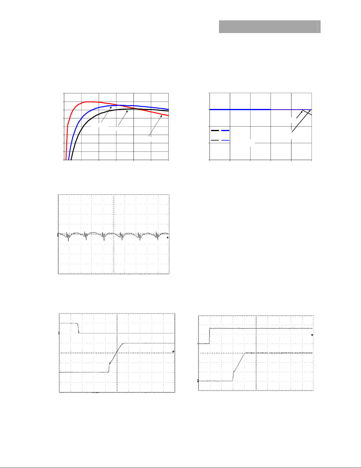
Characteristic Curves
The following figures provide typical characteristics for the 6A Analog PicoDLynxTM at 0.6Vo and 25oC.
90
85
80
75
70
65
60
EFFICIENCY, η (%)
55
50
0123456
Vin=6V
Vin=8V
Vin=3.3V
OUTPUT CURRENT, IO (A) AMBIENT TEMPERATURE, TA OC
Figure 1. Converter Efficiency versus Output Current.
6.5
6.0
5.5
5.0
Standard Part
(85°C)
Ruggedized (D)
Part ( 105°C)
OUTPUT CURRENT, Io (A)
4.5
55 65 75 85 95 105
Figure 2. Derating Output Current versus Ambient Temperature
and Airflow.
0.5m/s
(100LFM)
NC
(V) (20mV/div)
O
UTPUT VOLTAGE
V
TIME, t (1μs/div) TIME, t (20μs /div)
Figure 3. Typical output ripple and noise (C
V
IN
= 8V, Io = I
(V) (5V/div)
ON/OFF
(V) (200mV/div) V
O
o,max,
).
=10F ceramic,
O
(V) (10mV/div)
O
(A) (2Adiv) V
O
I
OUTPUT CURRENT, OUTPUT VOLTAGE
Figure 4. Transient Response to Dynamic Load Change from 50%
to 100% at 8Vin, Cout-1x47uF+4x330uF, CTune-33nF, RTune-178
(V) (5V/div)
IN
(V) (200mV/div) V
O
OUTPUT VOLTAGE ON/OFF VOLTAGE
V
Figure 5. Typical Start-up Using On/Off Voltage (Io = I
TIME, t (2ms/div) TIME, t (2ms/div)
o,max
). Figure 6. Typical Start-up Using Input Voltage (VIN = 8V, Io = I
OUTPUT VOLTAGE INPUT VOLTAGE
V
o,max
December 7, 2012 ©2012 General Electric Company. All rights reserved. Page 6
).
GE
Preliminary Data Sheet
6A Analog PicoDLynxTM: Non-Isolated DC-DC Power Modules
3Vdc –14.4Vdc input; 0.6Vdc to 5.5Vdc output; 6A Output Current
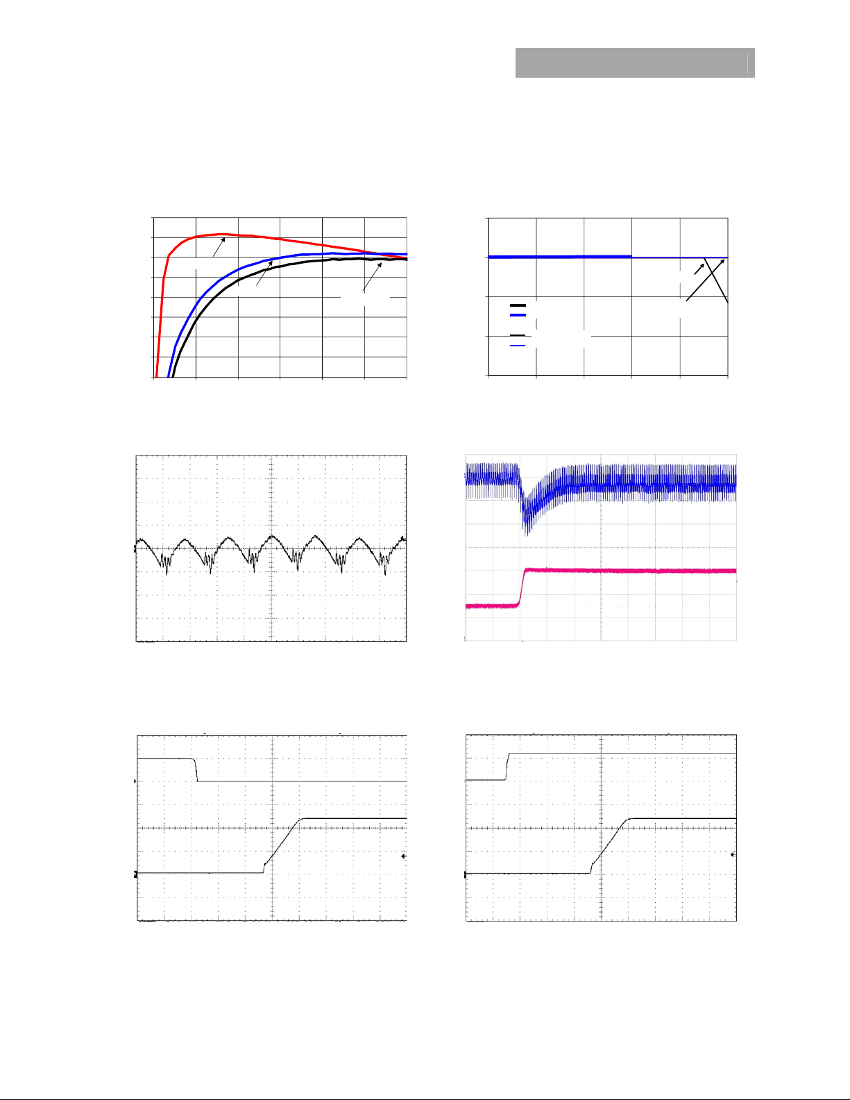
Characteristic Curves
The following figures provide typical characteristics for the 6A Analog PicoDLynxTM at 1.2Vo and 25oC.
95
90
EFFICIENCY, η (%)
85
80
75
70
65
60
55
Vin=3.3V
Vin=12V
0123456
Vin=14.4V
OUTPUT CURRENT, IO (A) AMBIENT TEMPERATURE, TA OC
Figure 7. Converter Efficiency versus Output Current.
6.5
6.0
5.5
5.0
Standard
Part (85 C)
Ruggediz ed (D)
Part (105°C)
OUTPUT CURRENT, Io (A)
4.5
55 65 75 85 95 105
Figure 8. Derating Output Current versus Ambient
Temperature and Airflow.
NC
0.5m/s
(100LFM)
(V) (20mV/div)
O
V
OUTPUT VOLTAGE
TIME, t (1μs/div) TIME, t (20μs /div)
Figure 9. Typical output ripple and noise (C
V
IN
= 12V, Io = I
(V) (5V/div)
ON/OFF
(V) (500mV/div) V
O
OUTPUT VOLTAGE ON/OFF VOLTAGE
V
o,max,
).
TIME, t (2ms/div) TIME, t (2ms/div)
=10F ceramic,
O
Figure 11. Typical Start-up Using On/Off Voltage (Io = I
o,max
(V) (10mV/div)
O
(A) (2Adiv) V
O
I
OUTPUT CURRENT, OUTPUT VOLTAGE
Figure 10. Transient Response to Dynamic Load Change
from 50% to 100% at 12Vin, Cout-1x47uF+3x330uF, CTune-
12nF & RTune-178
(V) (10V/div)
IN
(V) (500mV/div) V
).
O
OUTPUT VOLTAGE INPUT VOLTAGE
V
Figure 12. Typical Start-up Using Input Voltage (V
= I
o,max
).
IN
= 12V, I
o
December 7, 2012 ©2012 General Electric Company. All rights reserved. Page 7
 Loading...