

Fairchild Semiconductor MM74HC595WMX, MM74HC595SJX, MM74HC595SJ, MM74HC595MTCX, MM74HC595CW Datasheet
...
September 1983
Revised February 1999
MM74HC595 8-Bit Shift Registers with Output Latches
© 1999 Fairchild Semiconductor Corporation DS005342.prf www.fairchildsemi.com
MM74HC595
8-Bit Shift Registers with Output Latches
General Description
The MM74HC595 high speed shift register utilizes
advanced silicon-gate CM OS techn ology. This device possesses the high noise immunity and low power consumption of standard CM OS integrated circuits , as well as the
ability to drive 15 LS-TTL loads.
This device contains an 8-bit serial-in, parallel-out shift register that feeds an 8-b it D-type storage re gister. The storage register has 8 3-STATE outputs. Separate clocks are
provided for both the shift register and the storage register.
The shift register has a dire ct-overridin g clear, serial input,
and serial output (standa rd) pins for cascading. Both the
shift register and storag e register use positive-edge triggered clocks. If both clocks are connected together, the
shift register state will always be one clock pulse ahead of
the storage register.
The 74HC logic family is speed, function, an d p in-o ut co mpatible with the sta ndard 74LS logic fami ly. All inputs are
protected from damage due to static discharge by inte rnal
diode clamps to V
CC
and ground.
Features
■ Low quiescent current: 80 µA maximum (74HC Series)
■ Low input current: 1 µA maximum
■ 8-bit serial-in, parallel-out shift register with storage
■ Wide operating voltage range: 2V–6V
■ Cascadable
■ Shift register has direct clear
■ Guaranteed shift frequency: DC to 30 MHz
Ordering Code:
Devices also availab le in Tape and Reel. Specify by appending th e s uffix let t er “X” to the ordering cod e.
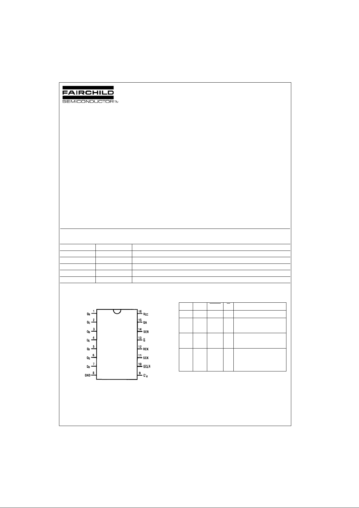
Connection Diagram
Pin Assignments f or DIP, SOIC, SOP and TSSOP
Top View
Truth Table
Order Number Package Number Package Description
MM74HC595M M16A 16-Lead Small Outline Integrated Circuit (SOIC), JEDEC MS-012, 0.150” Narrow
MM74HC595WM M16B 16-Lead Small Outline Integrated Circuit (SOIC), JEDEC MS-013, 0.300” Wide
MM74HC595SJ M16D 16-Lead Small Outline Package (SOP), EIAJ TYPE II, 5.3mm Wide
MM74HC595MTC MTC16 16-Lead Thin Shrink Small Outline Package (TSSOP), JEDEC MO-153, 4.4mm Wide
MM74HC595N N16E 16-Lead Dual-In-Line Package (PDIP), JEDEC MS-001, 0.300” Wide
RCK SCK SCLR G Function
XX XHQ
A
thru QH = 3-STATE
X X L L Shift Register cleared
Q
H
= 0
X ↑ H L Shift Register clocked
Q
N
= Q
n-1
, Q0 = SER
↑ X H L Contents of Shift
Register t ransferred
to output latches
www.fairchildsemi.com 2
MM74HC595
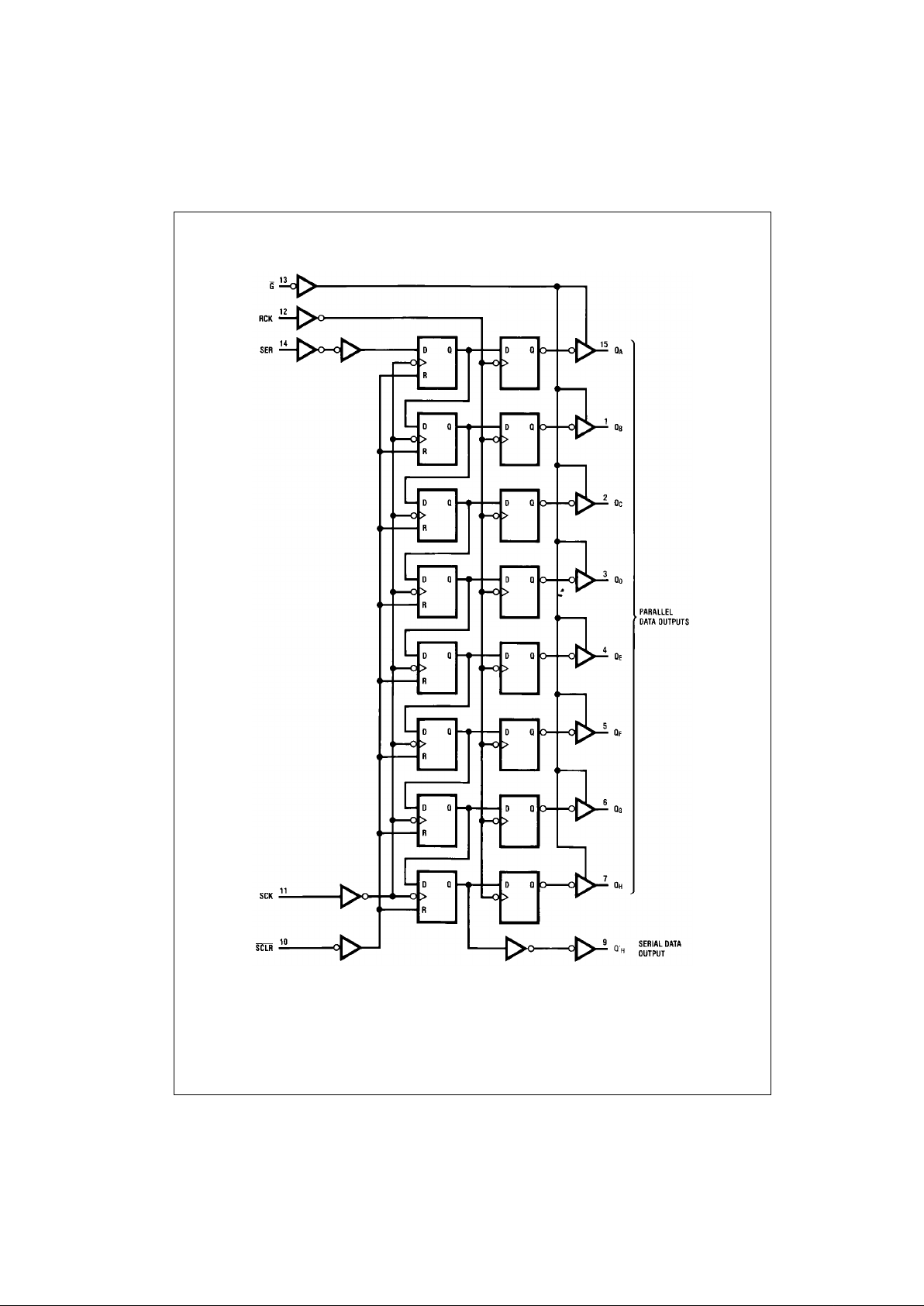
Logic Diagram
(positive logic)
3 www.fairchildsemi.com
MM74HC595
Absolute Maximum Ratings(Note 1)
(Note 2)
Recommended Operating
Conditions
Note 1: Absolute Maximum Ra tings are those valu es beyond w hich dam-
age to the device may occur.
Note 2: Unless otherwise specified all voltages are referenced to ground.
Note 3: Power Dissipation te mperature d erating — pl astic “N” pa ckage: −
12 mW/°C from 65°C to 85°C.
DC Electrical Characteristics (Note 4)
Note 4: For a powe r supply o f 5V ±10% the worst case output voltages (VOH, and VOL) occur for HC at 4.5V. Thus the 4. 5V valu es shou ld be u sed when
designing with this supply. Worst case V
IH
and VIL occur at V
CC
= 5.5V and 4.5V respectively. (The VIH value at 5.5V is 3 .8 5V.) The worst c as e leakage cur-
rent (I
IN
, ICC, and IOZ) occur for CMOS at the higher voltage and so th e 6. 0V values should be used.
Supply Voltage (VCC) −0.5 to +7.0V
DC Input Voltage (V
IN
) −1.5 to V
CC
+1.5V
DC Output Voltage (V
OUT
) −0.5 to V
CC
+0.5V
Clamp Diode Current (I
IK
, IOK) ±20 mA
DC Output Current, per pin (I
OUT
) ±35 mA
DC V
CC
or GND Current,
per pin (I
CC
) ±70 mA
Storage Temperature Range (T
STG
) −65°C to +150°C
Power Dissipation (P
D
)
(Note 3) 600 mW
S.O. Package only 500 mW
Lead Temperature (T
L
)
(Soldering 10 seconds) 260°C
Min Max Units
Supply Voltage (V
CC
)26V
DC Input or Output Voltage
(V
IN
, V
OUT
)0V
CC
V
Operating Temperature Range (T
A
) −40 +85 °C
Input Rise or Fall Times
(t
r
, tf) V
CC
= 2.0V 1000 ns
V
CC
= 4.5V 500 ns
V
CC
= 6.0V 400 ns
Symbol Parameter Conditions
V
CC
TA = 25°CTA = −40 to 85°CTA = −55 to 125°C
Units
Typ Guaranteed Limits
V
IH
Minimum HIGH Level 2.0V 1.5 1.5 1.5 V
Input Voltage 4.5V 3.15 3.15 3.15 V
6.0V 4.2 4.2 4.2 V
V
IL
Maximum LOW Level 2.0V 0.5 0.5 0.5 V
Input Voltage 4.5V 1.35 1.35 1.35 V
6.0V 1.8 1.8 1.8 V
V
OH
Minimum HIGH Level V
IN
= VIH or V
IL
Output Voltage |I
OUT
| ≤ 20 µA 2.0V 2.0 1.9 1.9 1.9 V
4.5V 4.5 4.4 4.4 4.4 V
6.0V 6.0 5.9 5.9 5.9 V
Q
H
V
IN
= VIH or V
IL
|I
OUT
| ≤ 4.0 mA 4.5V 4.2 3.98 3.84 3.7 V
|I
OUT
| ≤ 5.2 mA 6.0V 5.2 5.48 5.34 5.2 V
QA thru Q
H
V
IN
= VIH or V
IL
|I
OUT
| ≤ 6.0 mA 4.5V 4.2 3.98 3.84 3.7 V
|I
OUT
| ≤ 7.8 mA 6.0V 5.7 5.48 5.34 5.2 V
V
OL
Maximum LOW Level V
IN
= VIH or V
IL
Output Voltage |I
OUT
| ≤ 20 µA 2.0V 0 0.1 0.1 0.1 V
4.5V 0 0.1 0.1 0.1 V
6.0V 0 0.1 0.1 0.1 V
Q
H
V
IN
= VIH or V
IL
|I
OUT
| ≤ 4 mA 4.5V 0.2 0.26 0.33 0.4 V
|I
OUT
| ≤ 5.2 mA 6.0V 0.2 0.26 0.33 0.4 V
QA thru Q
H
V
IN
= VIH or V
IL
|I
OUT
| ≤ 6.0 mA 4.5V 0.2 0.26 0.33 0.4 V
|I
OUT
| ≤ 7.8 mA 6.0V 0.2 0.26 0.33 0.4 V
I
IN
Maximum Input V
IN
= VCC or GND 6.0V ±0.1 ±1.0 ±1.0 µA
Current
I
OZ
Maximum 3-STATE V
OUT
= VCC or GND 6.0V ±0.5 ±5.0 ±10 µA
Output Leakage
G = V
IH
I
CC
Maximum Quiescent V
IN
= VCC or GND 6.0V 8.0 80 160 µA
Supply Current I
OUT
= 0 µA
 Loading...