

Fairchild Semiconductor MM74HC573WM, MM74HC573WMX, MM74HC573SJ, MM74HC573MTC, MM74HC573MTCX Datasheet
...
© 2000 Fairchild Semiconductor Corporation DS005212 www.fairchildsemi.com
September 1983
Revised May 2000
MM74HC573 3-STATE Octal D-Type Latch
MM74HC573
3-STATE Octal D-Type Latch
General Description
The MM74HC573 high speed octal D-type latches utilize
advanced silicon-gate P-well CMOS technology. They possess the high noise immun ity and low powe r consumption
of standard CMOS integrated circuits, a s we ll as th e ability
to drive 15 LS-TTL loads. Due to the large ou tput drive
capability and the 3-STATE feature, these devices are ideally suited for interfacing with bus lines in a bus organized
system.
When the LATCH ENABLE(LE) input is HIGH, the Q ou tputs will follow the D inputs. When the LATCH ENABLE
goes LOW, data at the D inputs will be retained at the outputs until LATCH ENABLE returns HIGH again. Wh en a
HIGH logic level is applied to the OUTPUT CONTROL OC
input, all outputs go to a HIGH impedance state, regardless
of what signals are present at the other inputs and the state
of the storage elements.
The 74HC logic family is speed, functi on and pinout compatible with the sta ndard 74LS logic fam ily. All inputs are
protected from damage due to stati c discharge by i nternal
diode clamps to V
CC
and ground.
Features
■ Typical propagation delay: 18 ns
■ Wide operating voltage range: 2 to 6 volts
■ Low input current: 1
µA maximum
■ Low quiescent current: 80
µA maximum (74 HC Series)
■ Compatible with bus-oriented systems
■ Output drive capability: 15 LS-TTL loads
Ordering Code:
Devices also availab le in Tape and Reel. Specify by appending th e s uffix let t er “X” to the ordering code.
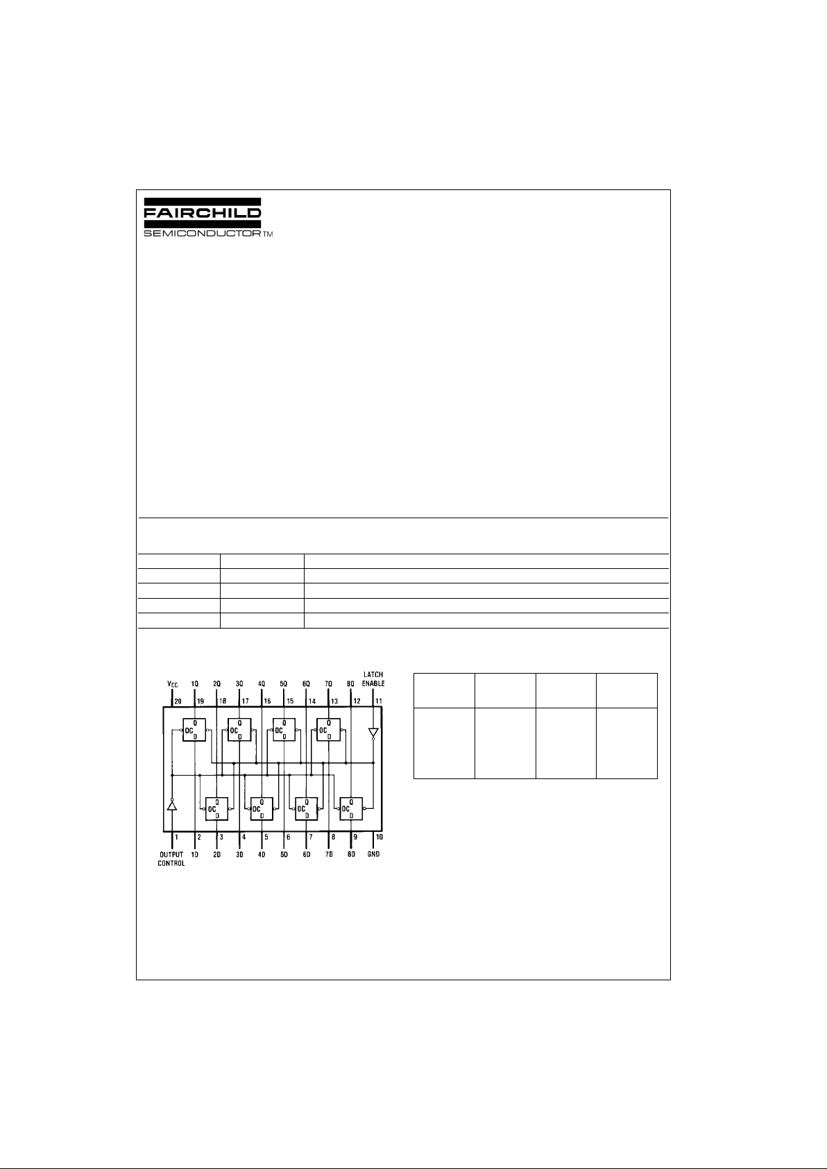
Connection Diagram
Top View
Truth Table
H = HIGH Level
L = LOW Level
Q0 = Level of output before steady-state inpu t conditions were establis hed.
Z = High Impedance
X = Don't Care
Order Number Package Number Package Description
MM74HC573WM M20B 20-Lead Small Outline Integrated Circuit (SOIC), JEDEC MS-013, 0.300 Wide
MM74HC573SJ M20D 20-Lead Small Outline Package (SOP), EIAJ TYPE II, 5.3mm Wide
MM74HC573MTC MTC20 20-Lead Thin Shrink Small Outline Package (TSSOP), JEDEC MO-153, 4.4mm Wide
MM74HC573N N20A 20-Lead Plastic Dual-In-Line Package (PDIP), JEDEC MS-001, 0.300 Wide
Output Latch Data Output
Control Enable
LHHH
LHLL
LLXQ
0
HXXZ

www.fairchildsemi.com 2
MM74HC573
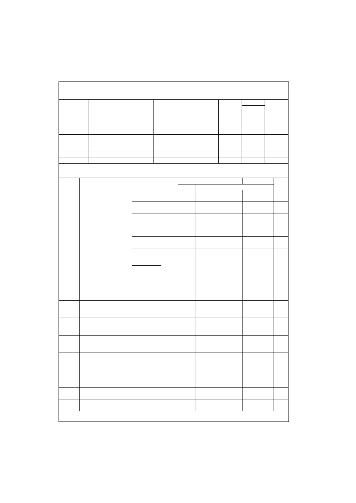
Absolute Maximum Ratings(Note 1)
(Note 2)
Recommended Operating
Conditions
Note 1: Absolute Maximum Ratings a re those va lues beyon d which d am-
age to the device may occur.
Note 2: Unless otherwise s pec ified all voltages are referenced to ground.
Note 3: Power Dissipa tion temp era ture dera ting — plastic “N” package: −
12 mW/°C from 65°C to 85°C.
DC Electrical Characteristics (Note 4)
Note 4: For a power supply of 5V ±1 0% the w orst-c ase ou tput vol tages (VOH, and VOL) occur for HC at 4.5V. Thus the 4. 5V valu es shoul d be use d when
designing with this supply. Worst-case V
IH
and VIL occur at V
CC
= 5.5V and 4.5V respectively. (The VIH value at 5.5V is 3.85V.) The worst-case leakage cur-
rent (I
IN
, ICC, and IOZ) occur for CMOS at the higher voltage and so th e 6. 0V values should be use d.
Supply Voltage (VCC) −0.5 to +7.0V
DC Input Voltage (V
IN
) −1.5 to V
CC
+1.5V
DC Output Voltage (V
OUT
) −0.5 to V
CC
+0.5V
Clamp Diode Current (I
IK
, IOK) ±20 mA
DC Output Current, per pin (I
OUT
) ±35 mA
DC V
CC
or GND Current, per pin (ICC) ±70 mA
Storage Temperature Range (T
STG
) −65°C to +150°C
Power Dissipation (P
D
)
(Note 3) 600 mW
S.O. Package only 500 mW
Lead Temper ature (T
L
)
(Solderi ng 10 seconds) 260
°C
Min Max Units
Supply Voltage (V
CC
)26V
DC Input or Output Voltage 0 V
CC
V
(V
IN
, V
OUT
)
Operating Temperature Range (T
A
) −40 +85 °C
Input Rise or Fall Times
(t
r
, tf) V
CC
= 2.0V 1000 ns
V
CC
= 4.5V 500 ns
V
CC
= 6.0V 400 ns
Symbol Parameter Conditions
V
CC
TA = 25°CTA = −40 to 85°CTA = −55 to 125°C
Units
Typ Guaranteed Limits
V
IH
Minimum HIGH Level Input 2.0V 1.5 1.5 1.5 V
Voltage 4.5V 3.15 3.15 3.15 V
6.0V 4.2 4.2 4.2 V
V
IL
Maximum LOW Level Input 2.0V 0.5 0.5 0.5 V
Voltage 4.5V 1.35 1.35 1.35 V
6.0V 1.8 1.8 1.8 V
V
OH
Minimum HIGH Level Output V
IN
= VIH or V
IL
Voltage |I
OUT
| ≤ 20 µA 2.0V 2.0 1.9 1.9 1.9 V
4.5V 4.5 4.4 4.4 4.4 V
6.0V 6.0 5.9 5.9 5.9 V
V
IN
= VIH or V
IL
|I
OUT
| ≤ 6.0 mA 4.5V 4.2 3.98 3.84 3.7 V
|I
OUT
| ≤ 7.8 mA 6.0V 5.7 5.48 5.34 5.2 V
V
OL
Maximum LOW Level Output V
IN
= VIH or V
IL
Voltage |I
OUT
| ≤ 20 µA 2.0V 0 0.1 0.1 0.1 V
4.5V 0 0.1 0.1 0.1 V
6.0V 0 0.1 0.1 0.1 V
V
IN
= VIH or V
IL
|I
OUT
| ≤ 6.0 mA 4.5V 0.2 0.26 0.33 0.4 V
|I
OUT
| ≤ 7.8 mA 6.0V 0.2 0.26 0.33 0.4 V
I
IN
Maximum Input Current V
IN
= VCC or GND 6.0V ±0.1 ±1.0 ±1.0 µA
I
OZ
Maximum 3-STATE Output V
OUT
= VCC or GND
Leakage Current OC = V
IH
6.0V ±0.5 ±5.0 ±10 µA
I
CC
Maximum Quiescent Supply V
IN
= VCC or GND
Current I
OUT
= 0 µA 6.0V 8.0 80 160 µA
∆I
CC
Quiescent Supply Current VCC = 5.5V OE 1.0 1.5 1.8 2.0 mA
per Input Pin VIN = 2.4V LE 0.6 0.8 1.0 1.1 mA
or 0.4V (Note 4) DATA 0.4 0.5 0.6 0.7 mA
3 www.fairchildsemi.com
MM74HC573
AC Electrical Characteristics
V
CC
= 5V, TA = 25°C, tr = t
f
= 6 ns
AC Electrical Characteristics
Symbol Parameter Conditions Typ
Guaranteed
Units
Limit
t
PHL
, t
PLH
Maximum Propagation Delay, Data to Q CL = 45 pF 16 20 ns
t
PHL
, t
PLH
Maximum Propagation Delay, LE to Q CL = 45 pF 14 22 ns
t
PZH
, t
PZL
Maximum Output Enable Time RL = 1 kΩ 15 27 ns
C
L
= 45 pF
t
PHZ
, t
PLZ
Maximum Output Disable Time RL = 1 kΩ 13 23 ns
CL = 5 pF
t
S
Minimum Set Up Time, Data to LE 10 15 ns
t
H
Minimum Hold Time, LE to Data 2 5 ns
t
W
Minimum Pulse Width, LE or Data 10 16 ns
Symbol Parameter Conditions
V
CC
TA = 25°CTA = −40 to 85°CTA = −55 to 125°C
Units
Typ Guaranteed Limits
t
PHL
, t
PLH
Maximum Propagation CL = 50 pF 2.0V 45 110 138 165 ns
Delay Data to Q CL = 150 pF 2.0V 58 150 188 225 ns
CL = 50 pF 4.5V 17 22 28 33 ns
CL = 150 pF 4.5V 21 30 38 40 ns
CL = 50 pF 6.0V 15 19 24 29 ns
CL = 150 pF 6.0V 19 26 33 39 ns
t
PHL
, t
PLH
Maximum Propagation CL = 50 pF 2.0V 46 115 138 165 ns
Delay, LE to Q CL = 150 pF 2.0V 60 155 194 233 ns
CL = 50 pF 4.5V 14 23 29 35 ns
CL = 150 pF 4.5V 21 31 47 47 ns
CL = 50 pF 6.0V 12 20 25 30 ns
CL = 150 pF 6.0V 19 27 34 41 ns
t
PZH
, t
PZL
Maximum Output Enable RL = 1 kΩ
Time C
L
= 50 pF 2.0V 55 140 175 210 ns
CL = 150 pF 2.0V 67 180 225 270 ns
C
L
= 50 pF 4.5V 15 28 35 42 ns
C
L
= 150 pF 4.5V 24 36 45 54 ns
CL = 50 pF 6.0V 14 24 30 36 ns
CL = 150 pF 6.0V 22 31 39 47 ns
t
PHZ
, t
PLZ
Maximum Output Disable RL = 1 kΩ 2.0V 40 125 156 188 ns
Time CL = 50 pF 4.5V 13 25 31 38 ns
6.0V 12 21 27 32 ns
t
S
Minimum Set Up Time 2.0V 30 75 95 110 ns
Data to LE 4.5V 10 15 19 22 ns
6.0V 9 13 16 19 ns
t
H
Minimum Hold Time 2.0V 25 31 38 ns
LE to Data 4.5V 5 6 7 ns
6.0V 4 5 6 ns
t
W
Minimum Pulse Width LE, 2.0V 30 80 100 120 ns
or Data 4.5V 9 16 20 24 ns
6.0V 8 14 18 20 ns
t
TLH
, t
THL
Maximum Output Rise CL = 50 pF 2.0V 25 60 75 90 ns
and Fall Time, Clock 4.5V 7 12 15 18 ns
6.0V 6 10 13 15 ns
C
PD
Power Dissipation Capacitance OC = V
CC
5pF
(Note 5) (per latch) OC = GND 52 pF
C
IN
Maximum Input 5 10 10 10 pF
Capacitance
 Loading...