


Fairchild Semiconductor MM74HC165MTC, MM74HC165MTCX, MM74HC165MX, MM74HC165N, MM74HC165SJX Datasheet
...
September 1983
Revised February 1999
MM74HC165 Parallel-in/Serial-out 8-Bit Shift Register
© 1999 Fairchild Semiconductor Corporation DS005316.prf www.fairchildsemi.com
MM74HC165
Parallel-in/Serial-out 8-Bit Shift Register
General Description
The MM74HC165 h i gh sp ee d PARALLEL-IN/S E RIA L-O UT
SHIFT REGISTER utilizes advanced silicon-gate CMOS
technology. It has the low power consumption and high
noise immunity of standard CMOS integrated circuits,
along with the ability to drive 10 LS-TTL loads.
This 8-bit serial shift register shifts data from Q
A
to Q
H
when clocked. Parallel inputs to each stage are enabled by
a low level at the SHI FT/LOAD input. Also included is a
gated CLOCK in put and a comple mentary output fr om the
eighth bit.
Clocking is accomplished throu gh a 2-inp ut NOR ga te permitting one input to be used as a CLOCK INHIBIT function.
Holding either of the CL OCK inputs high in hibits clocking,
and holding either CLOCK input low with the SHIFT/LOAD
input high enables the othe r CLOCK input. Data transfer
occurs on the positive going edge of the clock. Parallel
loading is inhibited as long as the SHIFT/LOAD input is
HIGH. When taken LOW, data at the parallel inputs is
loaded directly into the re gister ind epend ent of the stat e of
the clock.
The 74HC logic family is functionally as well as pin-out
compatible with the standard 74LS logic family. All inputs
are protected from damage due to static discharge by internal diode clamps to V
CC
and ground.
Features
■ Typical propagation delay: 20 ns (clock to Q)
■ Wide operating supply voltage range: 2–6V
■ Low input current: 1 µA maximum
■ Low quiescent suppl y current: 80 µA maximum (74HC
Series)
■ Fanout of 10 LS-TTL loads
Ordering Code:
Devices also availab le in Tape and Reel. Specify by appending th e s uffix let t er “X” to the ordering cod e.
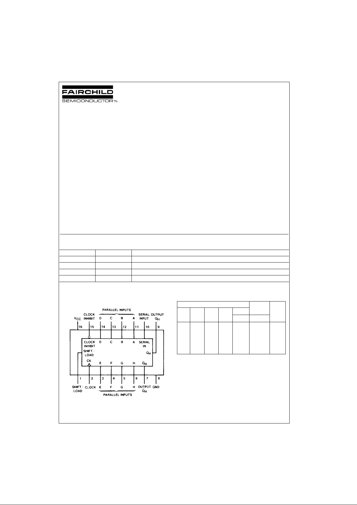
Connection Diagram
Pin Assignments f or DIP, SOIC, SOP and TSSOP
Top View
Function Table
H = HIGH Level (steady state), L = LOW Level (steady state)
X = Irrelevant (any input, inc luding transitions)
↑ = Transition from LOW-to-HIGH level
Q
A0
, QB0, QH0 = The lev el of QA, QB, or QH, respectively, before the indi-
cated steady-stat e input conditions were es t ablished.
Q
AN
, QGN = The level of QA or QG before the most recent ↑ transition of the
clock; indicates a one-bit shift.
Order Number Package Number Package Description
MM74HC165M M16A 16-Lead Small Outline Integrated Circuit (SOIC), JEDEC MS-012, 0.150” Narrow
MM74HC165SJ M16D 16-Lead Small Outline Package (SOP), EIAJ TYPE II, 5.3mm Wide
MM74HC165MTC MTC16 16-Lead Thin Shrink Small Outline Package (TSSOP), JEDEC MO-153, 4.4mm Wide
MM74HC165 N16E 16-Lead Plastic Dual-In-Line Package (PDIP), JEDEC MS-001, 0.300” Wide
Inputs Internal Output
Shift/ Clock
Clock Serial
Parallel
Outputs
Q
H
Load Inhibit
A. . .H Q
AQB
LXXXa...habh
HL LX XQ
A0QB0QH0
HL ↑ HXHQANQ
GN
HL ↑ LXLQANQ
GN
HHXX XQA0QB0Q
H0
www.fairchildsemi.com 2
MM74HC165
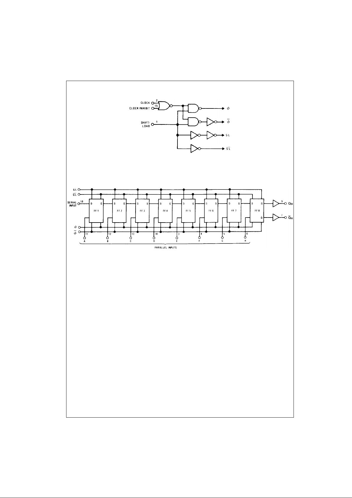
Logic Diagrams
3 www.fairchildsemi.com
MM74HC165
Absolute Maximum Ratings(Note 1)
(Note 2)
Recommended Operating
Conditions
Note 1: Absolute Maximum Ra tings are those valu es beyond w hich dam-
age to the device may occur.
Note 2: Unless otherwise specified all voltages are referenced to ground.
Note 3: Power Dissipation te mperature d erating — pl astic “N” pa ckage: −
12 mW/°C from 65°C to 85°C.
DC Electrical Characteristics (Note 4)
Note 4: For a powe r supply o f 5V ±10% the worst case output voltages (VOH, and VOL) occur for HC at 4.5V. Thus the 4. 5V valu es shou ld be u sed when
designing with this supply. Worst case V
IH
and VIL occur at V
CC
= 5.5V and 4.5V respectively. (The VIH value at 5.5V is 3 .8 5V.) The worst c as e leakage cur-
rent (I
IN
, ICC, and IOZ) occur for CMOS at the higher voltage and so th e 6. 0V values should be used.
Supply Voltage (VCC) −0.5 to +7.0V
DC Input Voltage (V
IN
) −1.5 to V
CC
+1.5V
DC Output Voltage (V
OUT
) −0.5 to V
CC
+0.5V
Clamp Diode Current (I
IK
, IOK) ±20 mA
DC Output Current, per pin (I
OUT
) ±25 mA
DC V
CC
or GND Current, per pin (ICC) ±50 mA
Storage Temperature Range (T
STG
) −65°C to +150°C
Power Dissipation (P
D
)
(Note 3) 600 mW
S.O. Package only 500 mW
Lead Temperature (T
L
)
(Solderi ng 10 seconds) 260°C
Min Max Units
Supply Voltage (V
CC
)26V
DC Input or Output Voltage
(V
IN
, V
OUT
)0V
CC
V
Operating Temperature Range (T
A
) −40 +85 °C
Input Rise or Fall Times
(t
r
, tf) V
CC
= 2.0V 1000 ns
V
CC
= 4.5V 500 ns
V
CC
= 6.0V 400 ns
Symbol Parameter Conditions
V
CC
TA = 25°CTA = −40 to 85°CTA = −55 to 125°C
Units
Typ Guaranteed Limits
V
IH
Minimum HIGH Level 2.0V 1.5 1.5 1.5 V
Input Voltage 4.5V 3.15 3.15 3.15 V
6.0V 4.2 4.2 4.2 V
V
IL
Maximum LOW Level 2.0V 0.5 0.5 0.5 V
Input Voltage 4.5V 1.35 1.35 1.35 V
6.0V 1.8 1.8 1.8 V
V
OH
Minimum HIGH Level V
IN
= VIH or V
IL
Output Voltage |I
OUT
| ≤ 20 µA 2.0V 2.0 1.9 1.9 1.9 V
4.5V 4.5 4.4 4.4 4.4 V
6.0V 6.0 5.9 5.9 5.9 V
V
IN
= VIH or V
IL
|I
OUT
| ≤ 4.0 mA 4.5V 4.2 3.98 3.84 3.7 V
|I
OUT
| ≤ 5.2 mA 6.0V 5.7 5.48 5.34 5.2 V
V
OL
Maximum LOW Level V
IN
= VIH or V
IL
Output Voltage |I
OUT
| ≤ 20 µA 2.0V 0 0.1 0.1 0.1 V
4.5V 0 0.1 0.1 0.1 V
6.0V 0 0.1 0.1 0.1 V
V
IN
= VIH or V
IL
|I
OUT
| ≤ 4.0 mA 4.5V 0.2 0.26 0.33 0.4 V
|I
OUT
| ≤ 5.2 mA 6.0V 0.2 0.26 0.33 0.4 V
I
IN
Maximum Input V
IN
= VCC or GND 6.0V ±0.1 ±1.0 ±1.0 µA
Current V
CC
= 2−6V
I
CC
Maximum Quiescent V
IN
= VCC or GND 6.0V 8.0 80 160 µA
Supply Current I
OUT
= 0 µA
V
CC
= 2−6V