

October 1987
Revised January 1999
MM74C164 8-Bit Parallel-Out Serial Shift Register
© 1999 Fairchild Semiconductor Corporation DS005896.prf www.fairchildsemi.com
MM74C164
8-Bit Parallel-Out Serial Shift Register
General Description
The MM74C164 shift registers are a monolithic complementary MOS (CMOS ) integrated circuit constructed w ith
N- and P-channel enhancement transistors. These 8-bit
shift registers have gated serial inputs and clear. Each register bit is a D-type master/slave flip-flop. A high-level input
enables the other input which will then determine the state
of the flip-flop.
Data is serially shifted in and out of the 8-bit register during
the positive going transition of c lock pulse. Clear is independent of the clock and accomplished by a low level at the
clear input. All inputs are protected against electrostatic
effects.
Features
■ Supply voltage range: 3V to 15V
■ Tenth power TTL comp atible: drive 2 LPTTL loads
■ High noise immunity: 0.45 V
CC
(typ.)
■ Low power: 50 nW (typ.)
■ Medium speed operation: 0.8 MHz (typ.) with 10V
supply
Applications
• Data terminals
• Instrumentation
• Medical electronics
• Alarm systems
• Industrial electronics
• Remote metering
• Computers
Ordering Code:
Devices also available in Tape and Reel. Specify by appending the suffix letter “X” to t he ordering code.
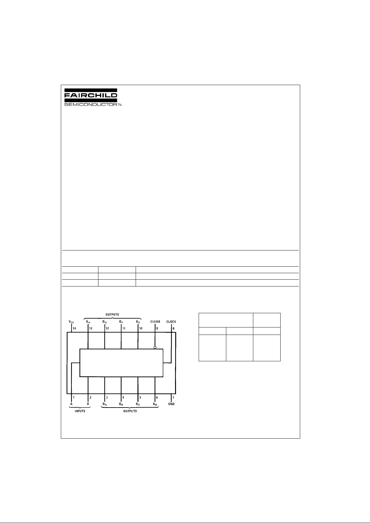
Connection Diagram
Pin Assignments for DIP and SOIC
Top View
Truth Table
Serial Inputs A and B
Order Number Package Number Package Description
MM74C164M M14A 14-Lead Small Outline Integrated Circuit (SOIC), JEDEC MS-120, 0.150” Narrow
MM74C164N N14A 14-Lead Plastic Dual-In-Line (PDIP), JEDEC MS-001, 0.300” Wide
Inputs Output
t
n
t
n+1
ABQ
A
111
010
100
000
www.fairchildsemi.com 2
MM74C164
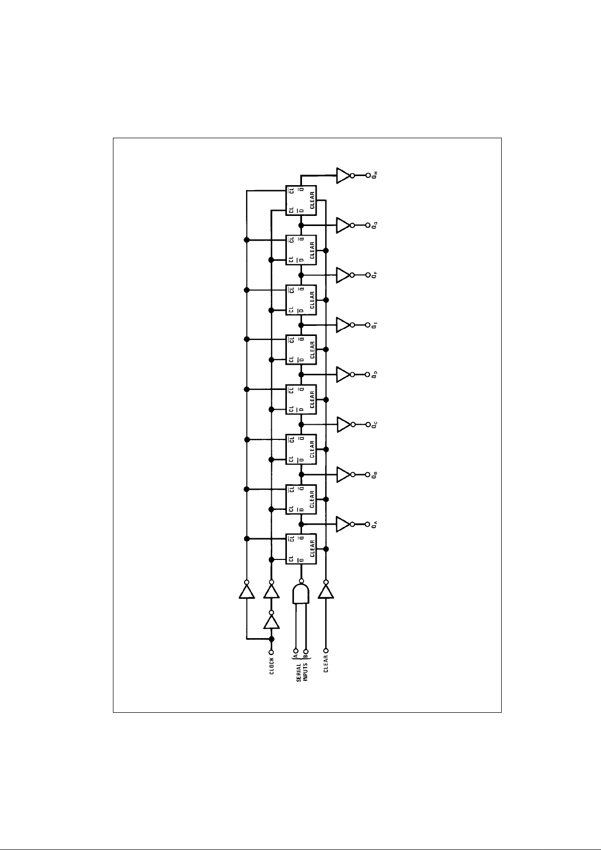
Block Diagram
3 www.fairchildsemi.com
MM74C164
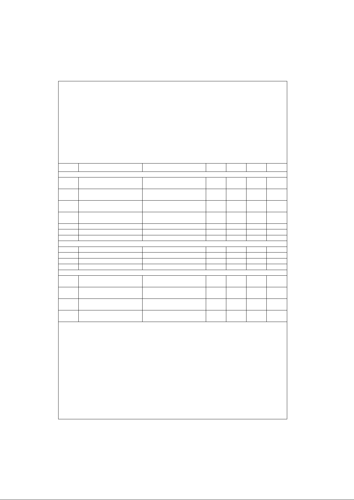
Absolute Maximum Ratings(Note 1)
Note 1: “Absolute Maximum Rat ings” are tho se values beyond which the
safety of the device cannot be guaranteed. E x c ept for “ Operating Temperature Range” they are not mea nt to imply that the devices sh ould be operated at these limits. The table of “Electrical Characteristics” provides
conditions for actual device o peration.
DC Electrical Characteristics
Min/Max limits apply across temperature range unless otherwise noted
Voltage at Any Pin −0.3V to VCC + 0.3V
Operating Temperature Range −40°C to +85°C
Storage Temperature Range −65°C to +150°C
Absolute Maximum V
CC
18V
Power Dissipation (P
D
)
Dual-In-Line 700 mW
Small Outline 500 mW
Operating V
CC
Range 3V to 15V
Lead Temperature
(soldering, 10 seconds) 260°C
Symbol Parameter Conditions Min Typ Max Units
CMOS TO CMOS
V
IN(1)
Logical “1” Input Voltage VCC = 5V 3.5 V
VCC = 10V 8.0 V
V
IN(0)
Logical “0” Input Voltage VCC = 5V 1.5 V
VCC = 10V 2.0 V
V
OUT(1)
Logical “1” Output Voltage VCC = 5V, IO = −10 µA4.5 V
VCC = 10V, IO = −10 µA9.0 V
V
OUT(0)
Logical “0” Output Voltage VCC = 5V, IO = +10 µA0.5V
VCC = 10V, IO = +10 µA1.0V
I
IN(1)
Logical “1” Input Current VCC = 15V, VIN = 15V 0.005 1.0 µA
I
IN(0)
Logical “0” Input Current VCC = 15V, VIN = 0V −1.0 −0.005 µA
I
CC
Supply Current VCC = 15V 0.05 300 µA
CMOS TO LPTTL INTERFACE
V
IN(1)
Logical “1” Input Voltage VCC = 4.75V VCC − 1.5 V
V
IN(0)
Logical “0” Input Voltage VCC = 4.75V 0.8 V
V
OUT(1)
Logical “1” Output Voltage VCC = 4.75V, IO = −360 µA2.4 V
V
OUT(0)
Logical “0” Output Voltage VCC = 4.75V, IO = 360 µA0.4V
OUTPUT DRIVE (See Family Characteristics Data Sheet) (Short Circuit Current)
I
SOURCE
Output Source Current VCC = 5V, V
IN(0)
= 0V −1.75 mA
TA = 25°C, V
OUT
= 0V
I
SOURCE
Output Source Current VCC = 10V, V
IN(0)
= 0V −8.0 mA
TA = 25°C, V
OUT
= 0V
I
SINK
Output Sink Current VCC = 5V, V
IN(1)
= 5V 1.75 mA
TA = 25°C, V
OUT
= V
CC
I
SINK
Output Sink Current VCC = 10V, V
IN(1)
= 10V 8.0 mA
TA = 25°C, V
OUT
= V
CC
 Loading...