Fairchild Semiconductor MM74C157N Datasheet

MM74C157
Quad 2-Input Multiplexers
MM74C157 Quad 2-Input Multiplexers
October 1987
Revised January 1999
General Description
The MM74C157 multiplexers are monolithic complementary MOS (CMOS) inte grated circuits constructed with Nand P-channel enhance ment transistors. They consist of
four 2-input multiplexers with common select and enable
inputs. When the enable input is at logi cal “0” the four outputs assume the values as selected from the inputs. When
the enab le in p ut i s at lo gi ca l “1 ” , th e o ut p ut s as s ume l og ic a l
“0”. Select decoding is done intern ally resulting in a single
select input only.
Features
■ Supply voltage range: 3V to 15V
■ High noise immunity: 0.45 V
■ Low power: 50 nW (typ.)
■ Tenth power TTL compatible: Drive 2 LPTTL loads
CC
(typ.)
Ordering Code:
Order Number Package Number Package Description
MM74C157N N16E 16-Lead Plastic Dual-In-Line Package (PDIP), JEDEC MS-001, 0.300” Wide
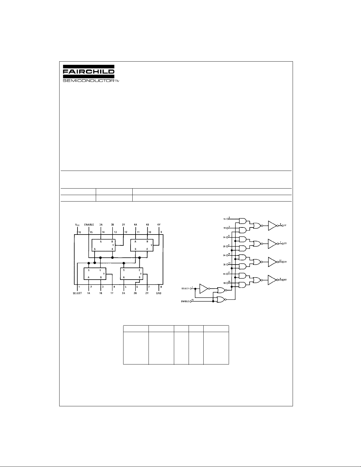
Connection Diagram
Pin Assignments for DIP
Logic Diagram
Top View
Truth Table
Enable Select A B Output Y
1XXX0
000X0
001X1
01X00
01X11
© 1999 Fairchild Semiconductor Corporation DS005894.prf www.fairchildsemi.com

Absolute Maximum Ratings(Note 1)
Voltage at Any Pin −0.3V to VCC + 0.3V
Operating Temperature Range −40°C to +85°C
Storage Temperature Range −65°C to +150°C
MM74C157
Maximum V
Power Dissipat ion (P
Dual-In-Line 700 mW
Small Outline 500 mW
Voltage 18V
CC
)
D
Operating V
Lead Temperature
(Soldering, 10 seconds)
260°C
Note 1: “Absolute Maxi mum Ratings” are those valu es beyond which the
safety of the device cannot be guaranteed. Exce pt for “O perating Temperature Range” they are not mean t to imply that the devices sho uld be operated at these limits. The table of “Electrical Characteristics” provides
conditions for actual device op eration.
Range 3V to 15V
CC
DC Electrical Characteristics
Min/Max limits apply across temperature range unless otherwise noted
Symbol Parameter Conditions Min Typ Max Units
CMOS TO CMOS
V
IN(1)
V
IN(0)
V
OUT(1)
V
OUT(0)
I
IN(1)
I
IN(0)
I
CC
CMOS TO TENTH POWER INTERFACE
V
IN(1)
V
IN(0)
V
OUT(1)
V
OUT(0)
OUTPUT DRIVE (See Family Characteristics Data Sheet) (Short Circuit Current)
I
SOURCE
I
SOURCE
I
SINK
I
SINK
Logical “1” Input Voltage VCC = 5V 3.5 V
VCC = 10V 8.0 V
Logical “0” Input Voltage VCC = 5V 1.5 V
VCC = 10V 2.0 V
Logical “1” Output Voltage VCC = 5V 4.5 V
VCC = 10V 9.0 V
Logical “0” Output Voltage VCC = 5V 0.5 V
VCC = 10V 1.0 V
Logical “1” Input Current VCC = 15V 0.005 1.0 µA
Logical “0” Input Current VCC = 15V −1.0 −0.005 µA
Supply Current VCC = 15V 0.05 60 µA
Logical “1” Input Voltage VCC = 4.75V VCC − 1.5 V
Logical “0” Input Voltage VCC = 4.75V 0.8 V
Logical “1” Output Voltage VCC = 4.75V, IO = −360 µA2.4 V
Logical “0” Output Voltage VCC = 4.75V, IO = 360 µA0.4V
Output Source Current VCC = 5V, V
TA = 25°C, V
Output Source Current VCC = 10V, V
TA = 25°C, V
Output Sink Current VCC = 5V, V
TA = 25°C, V
Output Sink Current VCC = 10V, V
TA = 25°C, V
= 0V −1.75 mA
IN(0)
= 0V
OUT
= 0V −8.0 mA
IN(0)
= 0V
OUT
= 5V 1.75 mA
IN(1)
= V
OUT
CC
= 10V 8.0 mA
IN(1)
= V
OUT
CC
www.fairchildsemi.com 2
 Loading...