

Fairchild Semiconductor KA7500C Datasheet
KA7500C
SMPS Controller
www.fairchildsemi.com
Features
• Internal Regulator Provides a Stable 5V Reference Supply
Trimmed to ±1% Accuracy.
• Uncommitted Output TR for 200mA Sink or Source
Current
• Output Control for Push-Pull or Single-Ended Operation
• Variable Duty Cycle by Dead Time Control (Pin 4)
Complete PWM Control Circuit
• On-Chip Oscillator With Master or Slave Operation
• Internal Circuit Prohibits Double Pulse at Either Output
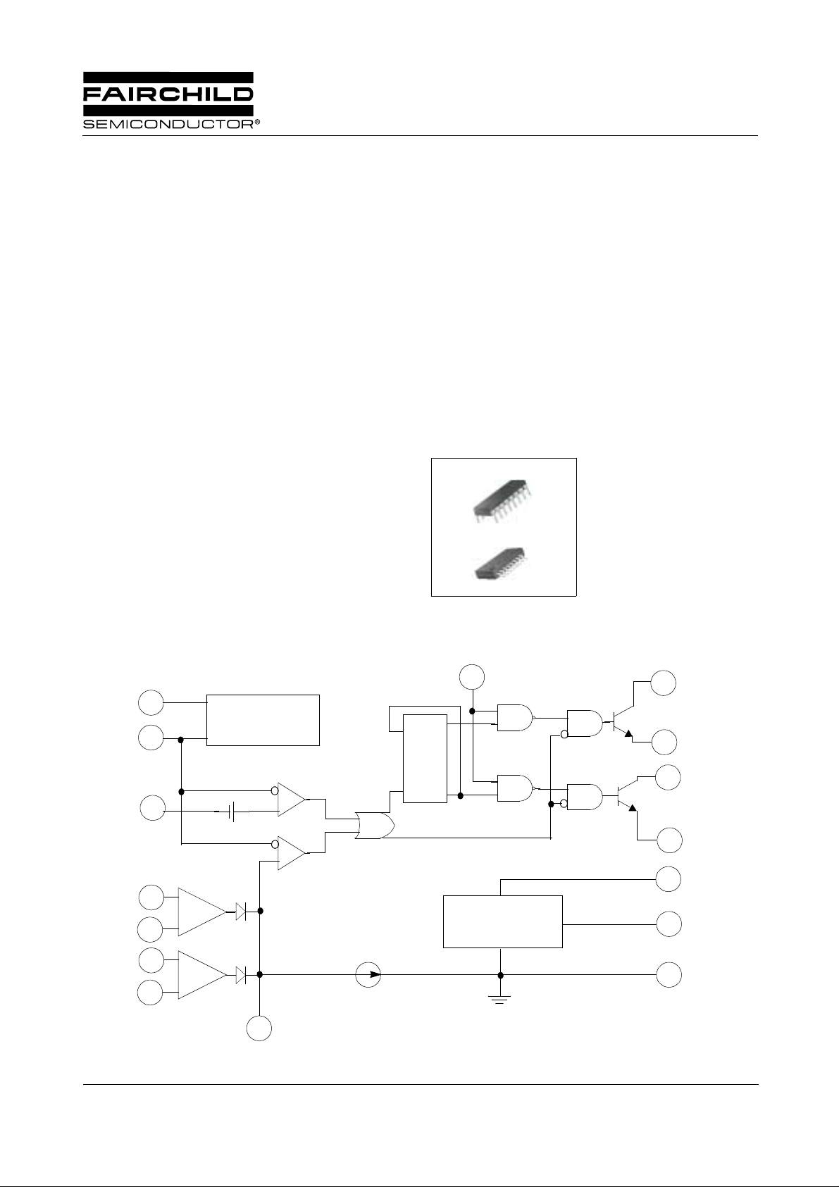
Internal Block Diagram
R
T
6
OSCILLATOR
5
C
T
Description
The KA7500C is used for the control circuit of the pulse
width modulation switching regulator. The KA7500C
consists of 5V reference voltage circuit, two error amplifiers,
flip flop, an output control circuit, a PWM comparator, a
dead time comparator and an oscillator. This device can be
operated in the switching frequency of 1kHz to 300kHz. The
precision of voltage reference (Vref) is improved up to ±1%
with trimming. This provides a better output voltage
regulation. The operating temperature range is
-25°C ~ +85°C.
16-DIP
13
1
1
C1
8
9
E1
16-SOP
OUTPUT CONTROL
D
Q
DEAD
TIME
CONTROL
EA(+)
EA(-)
EA(+)
EA(-)
©2003 Fairchild Semiconductor Corporation
16
15
4
1.2V
1
+
1
_
2
+
2
_
COMP INPUT
3
PWM
COMP
0.7MA
CK
Q
REFERENCE
5V
BAND GAP
11
10
12
14
7
C2
E2
V
CC
V
REF
GND
Rev. 1.0.1
KA7500C
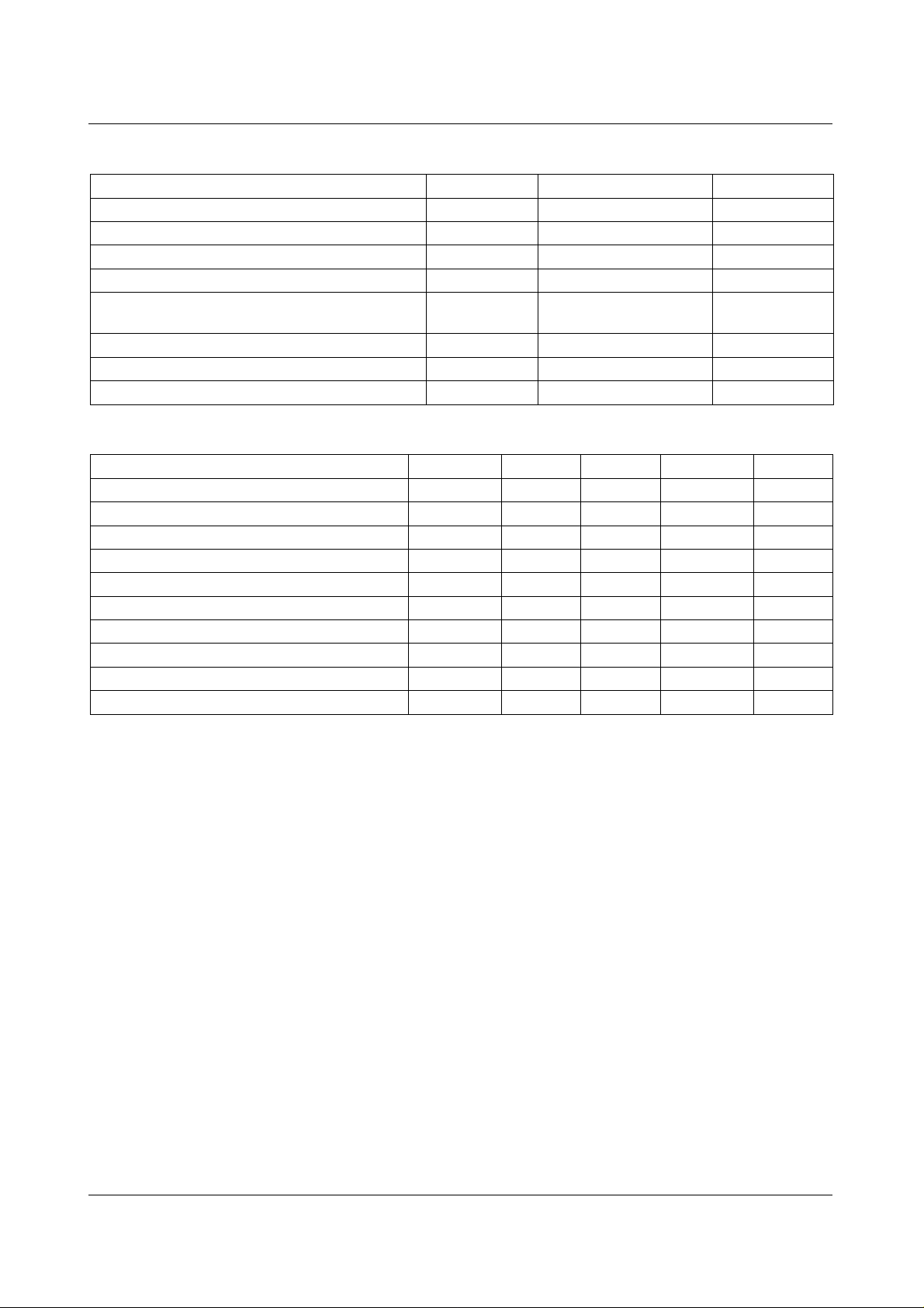
Absolute Maximum Ratings
Parameter Symbol Value Unit
Supply Voltage V
Collector Supply Voltage V
Output Current I
Amplifier Input Voltage V
Power Dissipation (T
Operating Temperature Range T
Storage Temperature Range T
= 25°C) P
A
OPR
STG
Junction Temperature T
CC
C
O
IN
D
j
42 V
42 V
250 mA
V
+0.3 V
CC
1 (KA7500C)
0.9 (KA7500CD)
-25 ~ +85 °C
-65 ~ +150 °C
125 °C
W
Recommended Operating Conditions
Parameter Symbol Min. Typ. Max. Unit
Power Supply Voltage V
Collector Output Voltage V
Collector Output Current (Each Transistor) I
Amplifier Input Voltage V
Current Into Feedback Terminal I
Reference Output Current I
Timing Resistor R
Timing Capacitor C
Oscillator Frequency f
CC
C1,VC2
C1,IC2
IN
fb
ref
T
T
osc
PWM Input Voltage (Pins3, 4, 13) - 0.3 - 5.3 V
7.0 15 40 V
-3040 V
- - 200 mA
0.3 - VCC-2.0 V
--0.3mA
--10mA
1.8 30 500 ΚΩ
0.0047 0.001 10 uF
1.0 40 200 kHz
2
KA7500C
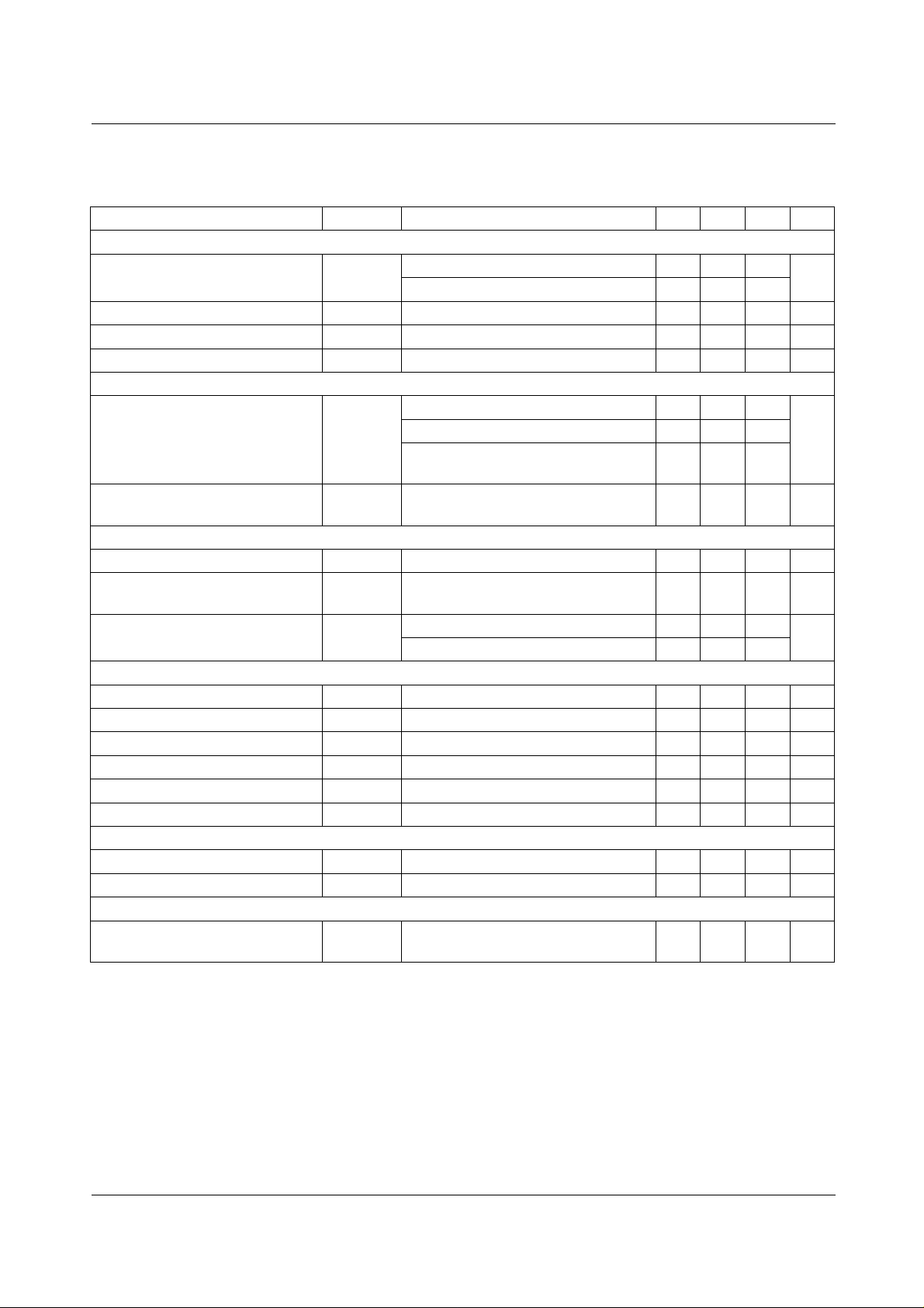
Electrical Characteristics
(VCC = 20V, f = 10kHz, TA = -25°C to +85°C, unless otherwise specified)
Parameter Symbol Conditions Min. Typ. Max. Unit
REFERENCE SECTION
I
= 1mA, TA=25°C(Note1) 4.95 5.0 5.05
Reference Output Voltage V
Line Regulation R
Load Regulation R
Short Circuit Output Current I
REF
Line
LOADIREF
SC
OSCILLATOR SECTION
Oscillation Frequency f
Frequency Change with
Temperature
osc
∆f/∆TC
DEAD TIME CONTROL SECTION
Input Bias Current I
Maximum Duty Cycle D
Input Threshold Voltage V
BIAS
(MAX)
ITH
ERROR AMP SECTION
Input Offset Voltage V
Input Offset Current I
Input Bias Current I
Common Mode Input Voltage V
Open-Loop Voltage Gain G
IO
IO
BIAS
CM
VO
Unit-Gain Bandwidth BW - - 650 - kHz
PWM COMPARATOR SECTION
Input Threshold Voltage V
Input Sink Current I
ITH
SINK
OUTPUT SECTION
Output Saturation Voltage
Common Emitter
V
CE(SAT)VE
REF
= 1mA 4.9 5.0 5.1
I
REF
VCC = 7V to 40V - 2.0 25 mV
= 1mA to 10mA - 1.0 15 mV
V
= 0V 10 35 50 mA
REF
CT = 0.001µF, RT = 30KΩ -40-
= 0.001µF, RT = 12KΩ,TA=25°C 9.2 10 10.8
C
T
= 0.001µF, RT = 30KΩ,
C
T
T
to T
A=Tlow
= 0.01µF, RT = 12KΩ --2%
T
high
9.0 - 12
VCC = 15V, 0V ≤ V4 ≤ 5.25V - -2.0 -10 µA
VCC = 15V, V4 = 0V
O.C Pin = V
REF
45 - - %
Zero Duty Cycle - 3.0 3.3
Max. Duty Cycle 0 - -
V3 = 2.5V - 2.0 10 mV
V3 = 2.5V - 25 250 mA
V3 = 2.5V - 0.2 1.0 µA
7V ≤ V
≤ 40V -0.3 - V
CC
CC
0.5V ≤ V3 ≤ 3 .5V 70 95 - dB
Zero Duty Cycle - 4 4.5 V
V3 = 0.7V -0.3 -0.7 - mA
= 0V, IC = 200mA - 1.1 1.3 V
V
kHz
V
V
3
 Loading...