Fairchild Semiconductor KA3883D, KA3883, KA3882D, KA3885D, KA3885 Datasheet
...
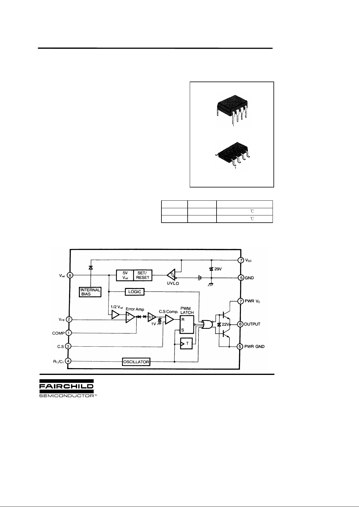
KA3882/3/4/5 SMPS CONTROLLER
CURRENT MODE PWM CONTROLLER
The KA3882/3/4/5 are fixed PWM controller for Off-Line and DC
to DC converter applications. The internal circuits include
UVLO,
low start up current circuit, temperature compensated
reference,
high
gain error amplifier, current sensing comparator, and high
current totempole output for driving a POWER MOSFET. Also KA
3882/3/4/5 provide low start up
current below 0.3mA and short
shutdown delay time typ. 100ns.
The
KA3882 and KA3884 have UVLO threshold of 1 6V(on) and 8 SOP
10V(off).
The KA3883 and KA3885 are 8.4V(on) and 7.6V(off).
The KA3882 and KA3883 can operate within 100% duty cycle.
The KA3884 and KA3885 within 50% by using T Flip-Flop.
FEATURES
• Low Start Current 0.2mA (typ)
• Operating Range Up To 500KHz
• Cycle by Cycle Current Limiting
ORDERING INFORMATI ON
• Under Voltage Lock Out With Hysteresis
• Short Shutdown Delay Time: typ.100ns
• High Current Totempole Output
• Output Swing Limiting: 22V
BLOCK DIAGRAM
Device Package Operating Temperature
KA388X 8 DIP
0 ~ + 85
Î
KA388XD 8 SOP
0 ~ + 85
Î
8 DIP
©1999 Fairchild Semiconductor Co rporation
Rev. B

KA3882/3/4/5 SMPS CONTROLLER
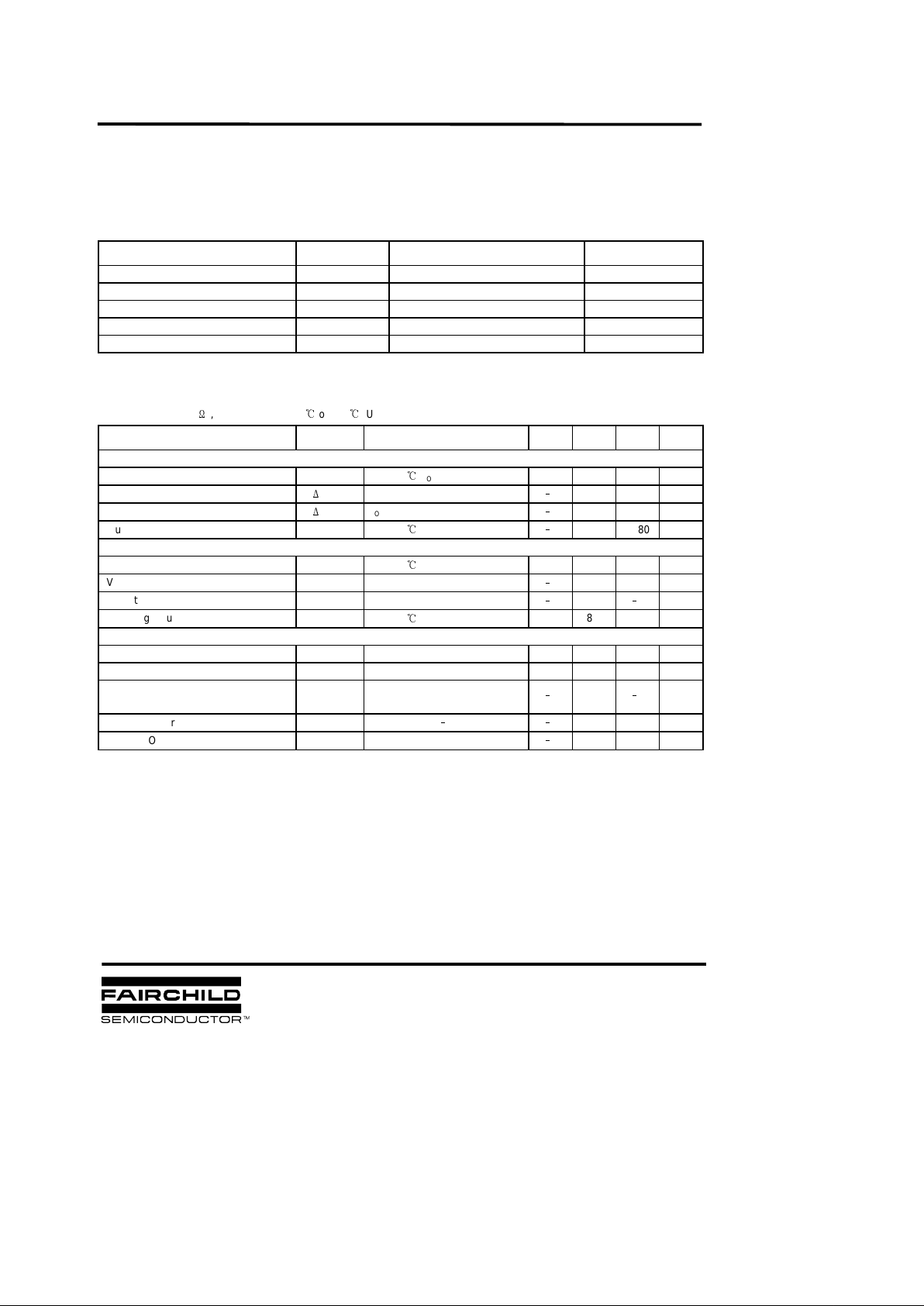
ABSOLUTE MAXIMUM RATINGS
ELECTRICAL CHARACTERISTICS
(VCC = 15V, RT = 10K`, CT = 3.3nF, TA = 0Îto + 85Î, Unless otherwise specified)
Characteristic Symbol Value Unit
Supply Voltage V
CC
30 V
Output Current I
O
+ 1 A
Analog Inputs (pin 2, 3) V
I(ANA)
- 0.3 to 6.3 V
Error Amp. Output Sink Current I
SINK(EA)
10 mA
Power Dissipation P
D
1W
Characteristic Symbol Test Conditions Min Typ Max Unit
REFERENCE SECTION
Output Voltage V
REF
TJ = 25Î, IO = 1mA
4.9 5.0 5.1 V
Line Regulation
L
V
REF
VCC = 12V to 25V
ï
620mV
Load Regulation
L
V
REF
IO = 1mA to 20mA
ï
625mV
Output Short Circuit I
SC
Ta = 25
Î
ï
- 100 - 180 mA
OSILLATOR SECTION
Initial Accuracy F
OSC
TJ = 25
Î
47 52 57 KHz
Voltage Stability ST
V
V
CC
= 12V to 25V
ï
0.2 1 %
Amplitude V
OSC
V
PIN4
, Peak to Peak
ï
1.7
ï
V
Discharge Current I
DISCHG
TJ = 25Î, Pin4 = 2V
7.8 8.3 8.8 mA
CURRENT SENSE SECTION
Gain G
V
(NOTE 2, 3) 2.85 3 3.15 V/V
Maximum Input Signal V
I(MAX)
V
PIN1
= 5V(NOTE 2) 0.9 1.0 1.1 V
PSRR PSRR
V
CC
= 12V to 25V
(NOTE 1, 2)
ï
70
ï
dB
Input Bias Current I
BIAS
ïï
- 2 -10 uA
Delay to Output T
D
V
PIN3
= 0V to 2V (NOTE1)
ï
100 200 ns
 Loading...