KA3846
SMPS Controller
www.fairchildsemi.com
Features
• Automatic Feed Forward Compensation
• Programmable Pulse by Pulse Current Limiting
• Automatic Symmetry Correction in Push-Pull
Configuration
• Enhanced Load Response Characteristics
• Parallel Operation Capability for Modulator Power
Systems
• Differential Current Sense Amplifier with Common Mode
Range
• Double Pulse Suppression
• 200mA Totem-Pole Outputs
• ±2% Band gap Reference
• Under-Voltage Lockout
• Soft-Start Capability
• Shutdown Terminal
• 500KHz Operation
Description
The KA3846 control IC provides all of the necessary features to implement fixed frequency, current mode control
schemes while maintaining a minimum external parts count.
The superior performance of this technique can be measured
in improved line regulation, enhanced load response characteristics, and a simpler, easier-to-design control loop.
Topological advantages include inherent pulse-by-pulse current limiting capability, automatic symmetry correction for
push-pull converters, and the ability to parallel “power
,,
module
circuitry includes built-in-under-voltage lockout and programmable current limit in addition to soft-start capability.
A shutdown function is also available which can initiate
either a complete shutdown with automatic restart or latch
the supply off. Other features include fully latched operation,
double pulse suppression, deadtime adjust capability, and
±2% trimmed bandgap reference. The KA3846 features low
outputs in the OFF state.
while maintaining equal current sharing. Protection
16-DIP
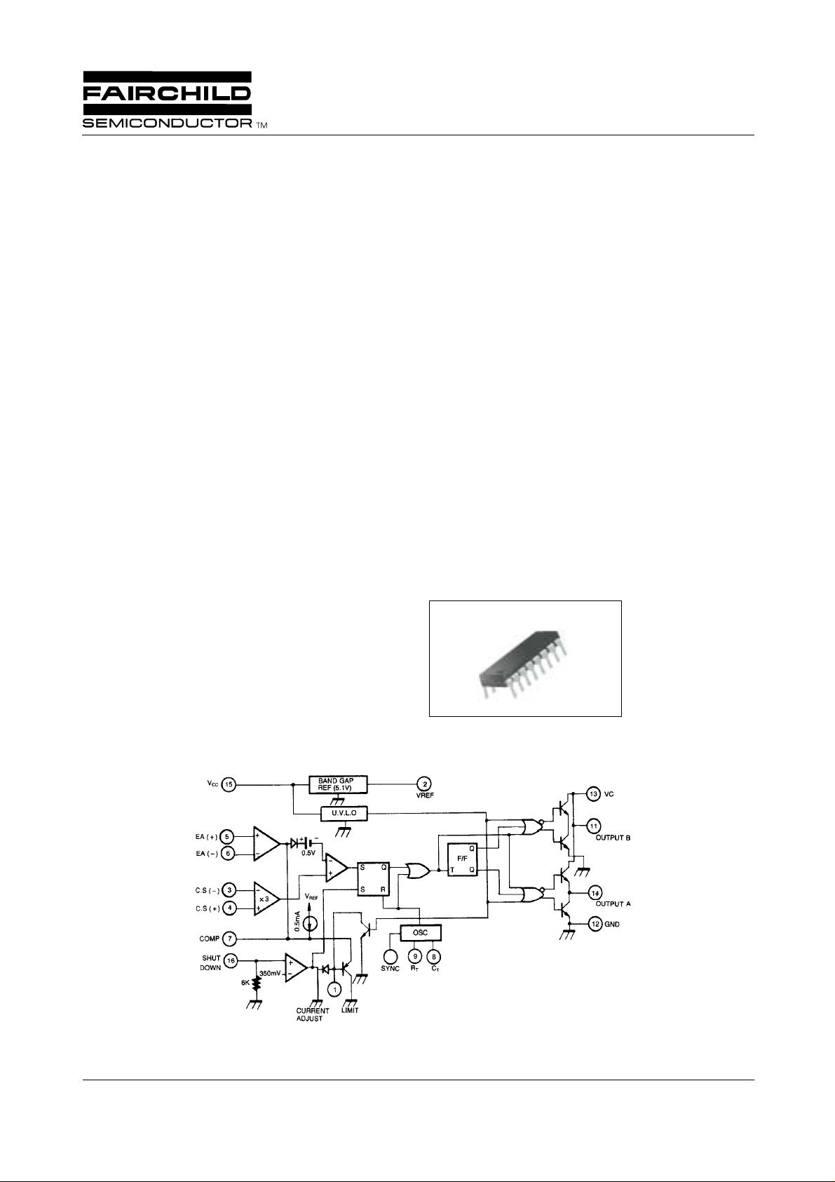
Internal Block Diagram
©2000 Fairchild Semiconductor International
1
10
Rev. 5.0

KA3846
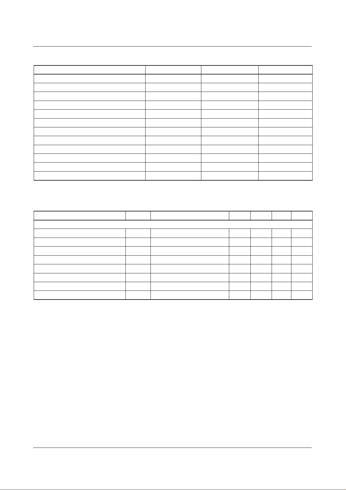
Absolute Maximum Ratings
Parameter Symbol Value Unit
Supply Voltage V
Collector Supply Voltage V
Output Current, Sink of Source (Peak) I
Reference Output Current I
Soft Start Sink Current I
Sync Output Current I
Error Amplifier Output Current I
Oscillator Changing Current I
Power Dissipation (T
= 25°C) P
A
CHG(OSC)
Operating Temperature T
Storage Temperature T
Lead Temperature (Soldering, 10sec) T
Electrical Characteristics
(VCC=15V, TA=0°C to +70°C, unless otherwise specified)
CC
C
O
REF
SINK(S.S)
SYNC
O(E.A)
D
OPR
STG
LEAD
40 V
40 V
500 mA
30 mA
50 mA
5mA
5mA
5mA
1000 mW
0 ~ +70 °C
-65 ~ +150 °C
+300 °C
Parameter Symbol Conditions Min. Typ. Max. Unit
REFERENCE SECTION
Reference Output Voltage V
REF
Line Regulation ∆V
Load Regulation ∆V
Temperature Stability(Note 6) ST
Output Voltage Range (Note 6) V
Short Circuit Output Current I
REF
SC
Output Noise Voltage(Note 6) V
Long-Term Stability(Note 6) S
TJ = 25°C, I
VCC = 8 to 40V - 5 20 mV
REF
REF IREF
T
Line,Load,Temp 4.95 - 5.25 V
V
REF
NO
f = 10Hz to 10KHz, TJ = 25°C - 100 - uV
TJ = 125°C, 1KHz 2 5 8 mV
T
= 1mA 5.00 5.10 5.20 V
REF
1 to 10mA - 3 15 mV
- -0.41.0mV/°C
= 0V -10 -45 - mA
2

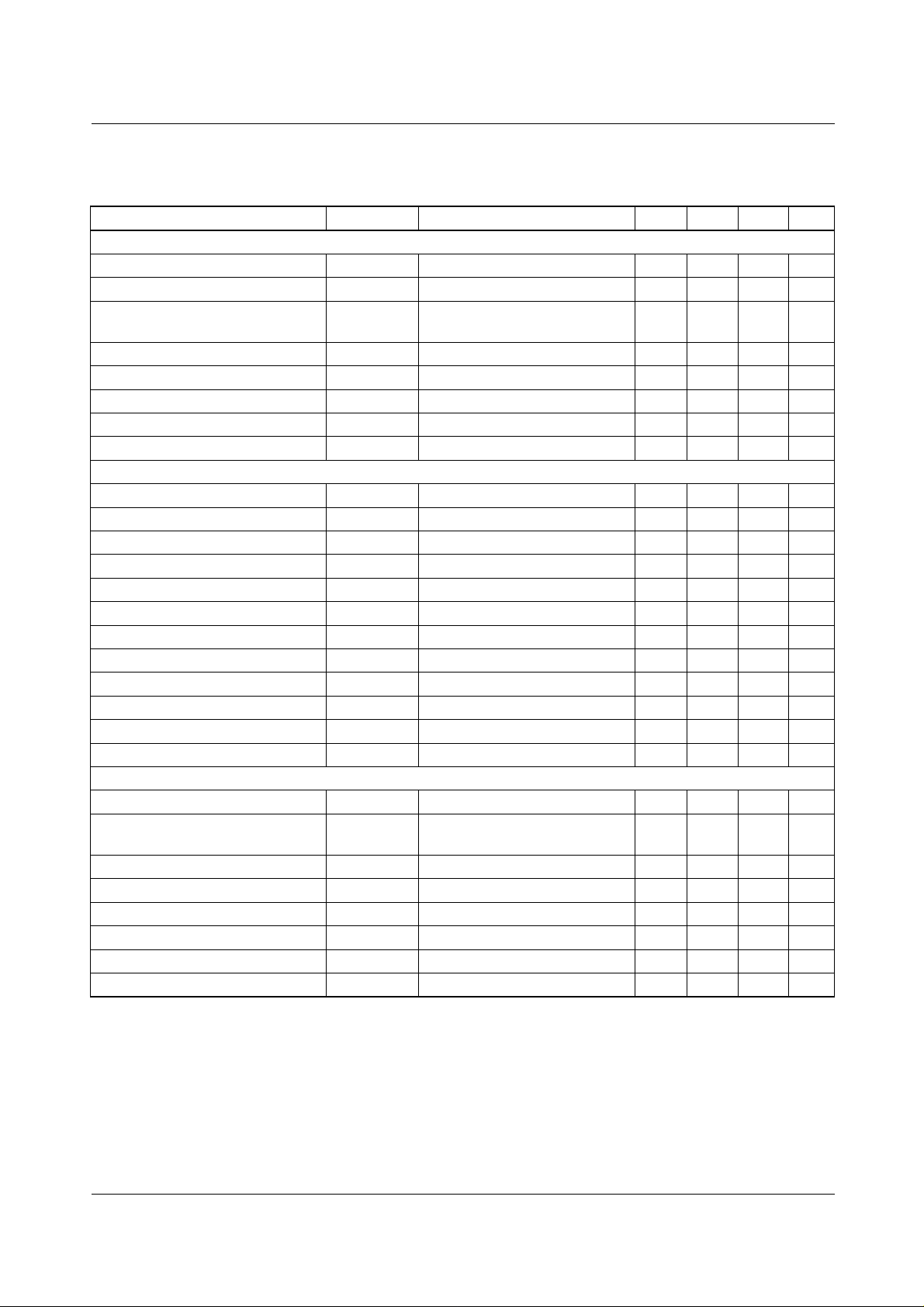
Electrical Characteristics
(VCC= 15V,TA=0°C to +70°C, unless otherwise specified)
Parameter Symbol Conditions Min. Typ. Max. Unit
OSCILLATOR SECTION (Note 2)
Initial Accuracy ACCUR T
Frequency Change with Voltage ∆f/∆V
Frequency Change with
Temperature (Note 6)
Sync Output High Level V
Sync Output Low Level V
Sync Input High Level V
Sync Input Low Level V
Sync Input Current I
ERROR AMPLIFIER SECTION
Input Offset Voltage V
Input Bias Current I
Input Offset Current I
Common-Mode Range V
Open Loop Voltage Gain G
Unity Gain Bandwidth(Note 6) BW T
Common Mode Rejection Ratio CMRR V
Power Supply Rejection Ratio PSRR V
Output Sink Current I
Output Source Current I
High Output Voltage V
Low Output Voltage V
CURRENT SENSE AMPLIFIER SECTION
Amplifier Gain (Note 1, 3) G
Maximum Differential Input
Signal (V
- V3) (Note 1)
4
V
Input Offset Voltage (Note 1) V
Common Mode Rejection Ratio CMRR V
Power Supply Rejection Ratio PSRR V
Input Bias Current (Note 1) I
Input Offset Current (Note 1) I
Delay to Outputs (Note 6) t
CC
∆f/∆T - - 1-%
OH(SYNC)
OL(SYNC)
IH(SYNC)
IL(SYNC)
I(SYNC)
IO
BIAS
IO
CM
VO
SINK
SOURCE
OH
OL
V
I(DIFF,MAX) RL
IO
BIAS
IO
D
KA3846
= 25°C394347KHz
J
VCC = 8 to 40V - 1 2 %
- 3.9 4.35 - V
- -2.32.5V
V8 = 0V 3.9 - - V
V8 = 0V - - 2.5 V
Sync Voltage = 3.9V, V8 = 0V - 1.3 1.5 mA
- -0.55mV
- --0.6-1uA
- - 40 250 uA
VCC = 8 to 40V 0 - VCC2V
VO = 1.2 to 3V, V
= 25°C0.71.0-MHz
J
= 0 to 38V, VCC = 40V 75 100 - dB
CM
= 8 to 40V 80 105 - dB
CC
V
= -15mV to 5V, V7 = 2.5V 2 6 - mA
IO
= 2V 80 105 - dB
CM
RL = 15KΩ -0.4 -0.5 - mA
RL = 15KΩ 4.3 4.6 - V
- -0.71V
V3 = 0V, Pin 1 open 2.5 2.75 3.0 V
= 15KΩ, Pin 1 open 1.1 1.2 - V
V1 = 0.5V, Pin 1 open - 5 25 mV
= 1 to 12V 60 83 - dB
CM
= 8 to 40V 60 84 - dB
CC
V1 = 0.5V, Pin 7 open - -2.5 -10 uA
V1 = 0.5V, Pin 7 open - 0.08 1 uA
TJ = 25°C - 200 500 ns
3
 Loading...