Fairchild Semiconductor KA3845BD, KA3845B, KA3843BD, KA3843B, KA3842BD Datasheet
...
www.fairchildsemi.com
KA3842B/KA3843B/KA3844B/KA3845B
SMPS Controller
Features
• Low Start Up Current
• Maximum Duty Clamp
• UVLO With Hysteresis
• Operating Frequency Up To 500KHz
Description
The KA3842B/KA3843B/KA3844B/KA3845B are fixed
frequency current-mode PWM controller. They are specially designed for Off - Line and DC-to-DC converter
applications with minimum external components. These
integrated circuits feature a trimmed oscillator for precise
duty cycle control, a temperature compensated reference,
high gain error amplifier. current sensing comparator, and a
high current totempole output Ideally suited for driving a
power MOSFET. Protection circuity Includes built in
under-voltage lock out a nd cur re nt l imit ing. The KA3842B
and KA3844B have UVLO thresholds of 16V (on) and
10V (off) The KA3843B and KA3845B are 8.5V (on) and
7.9V (off) T he K A3842B and KA3843B c an operate within
100% duty cycle. The KA3844B and KA3845B can operate
with 50% duty cycle.
8-DIP
1
14-SOP
©2000 Fairchild Semiconductor International
1
Rev. 5.0

KA3842B/KA3843B/KA3844B/KA3845B
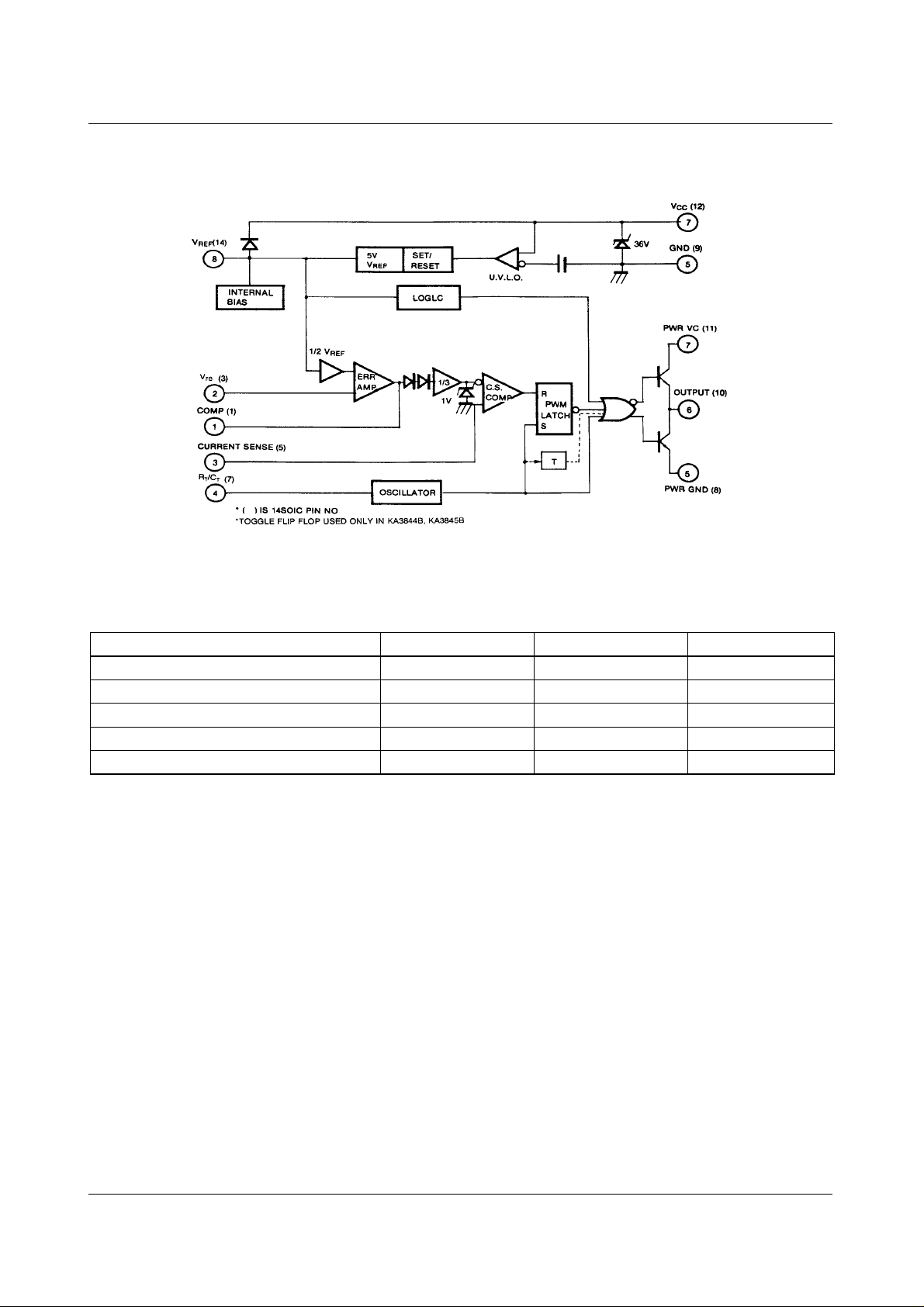
Internal Block Diagram
Absolute Maximum Ratings
Parameter Symbol Value Unit
Supply Voltage V
Output Current I
Analog Inputs (Pin 2.3) V
Error Amp Output Sink Current I
Power Dissipation (T
= 25°C) P
A
CC
O
(ANA)
SINK (E.A)
D
30 V
±1A
-0.3 to 6.3 V
10 mA
1W
2

Electrical Characteristics
(VCC=15V, RT=10KΩ, CT=3.3nF, TA= 0°C to +70°C, unless otherwise specified)
Parameter Symbol Conditions Min. Typ. Max. Unit
REFERENCE SECTION
Reference Output Voltage V
Line Regulation ∆V
Load Regulation ∆V
Short Circuit Output Current I
REF
REF
REF
SC
OSCILLATOR SECTION
Oscillation Frequency f T
Frequency Change with Voltage ∆f/∆V
Oscillator Amplitude V
OSC
ERROR AMPLIFIER SECTION
Input Bias Current I
Input Voltage V
Open Loop Voltage Gain G
BIAS
I(E>A)
VO
Power Supply Rejection Ratio PSRR 12V≤ V
Output Sink Current I
Output Source Current I
High Output Voltage V
Low Output Voltage V
SINK
SOURCE
OH
OL
CURRENT SENSE SECTION
Gain G
Maximum Input Signal V
V
I(MAX)
Power Supply Rejection Ratio PSRR 12V≤ V
Input Bias Current I
BIAS
OUTPUT SECTION
V
Low Output Voltage
High Output Voltage
Rise Time t
Fall Time t
OL
V
OH
R
F
UNDER-VOLTAGE LOCKOUT SECTION
Start Threshold
Min. Operating Voltage
(After Turn On)
V
TH(ST)
V
OPR(MIN)
TJ = 25°C, I
12V≤V
1mA≤I
CC
REF
= 1mA 4.90 5.00 5.10 V
REF
≤25V - 6 20 mV
≤20mA - 6 25 mV
TA = 25°C - -100 -180 mA
= 25°C475257KHz
J
CC
12V≤V
≤25V - 0.05 1 %
CC
- -1.6-V
- --0.1-2µA
V1 = 2.5V 2.42 2.50 2.58 V
2V≤ V
≤4V 65 90 - dB
O
≤25V 60 70 - dB
CC
V2 = 2.7V, V1 = 1.1V 2 7 - mA
V2 = 2.3V, V1 = 5V -0.6 -1.0 - mA
V2 = 2.3V, RL = 15KΩ to GND 5 6 - V
V2 = 2.7V, RL = 15KΩ to Pin 8 - 0.8 1.1 V
(Note 1 & 2) 2.85 3 3.15 V/V
V1 = 5V(Note 1) 0.9 1 1.1 V
≤25V (Note 1) - 70 - dB
CC
- --3-10µA
I
= 20mA - 0.08 0.4 V
SINK
= 200mA - 1.4 2.2 V
I
SINK
I
SOURCE
I
SOURCE
= 20mA 13 13.5 - V
= 200mA 12 13.0 - V
TJ = 25°C, CL= 1nF (Note 3) - 45 150 ns
TJ = 25°C, CL= 1nF (Note 3) - 35 150 ns
KA3842B/KA3844B 14.5 16.0 17.5 V
KA3843B/KA3845B 7.8 8.4 9.0 V
KA3842B/KA3844B 8.5 10.0 11.5 V
KA3843B/KA3845B 7.0 7.6 8.2 V
KA3842B/KA3843B/KA3844B/KA3845B
P-P
3

KA3842B/KA3843B/KA3844B/KA3845B
Electrical Characteristics (Continued)
(VCC=15V, RT=10KΩ, CT=3.3nF, TA= 0°C to +70°C unless otherwise specified)
Parameter Symbol Conditions Min. Typ. Max. Unit
PWM SECTION
Max. Duty Cycle
D
Min. Duty Cycle D
TOTAL STANDBY CURRENT
Start-Up Current I
Operating Supply Current I
CC(OPR)
Zener Voltage V
(max)
D KA3844B/KA3845B 47 48 50 %
(MIN)
ST
Z
KA3842B/KA3843B 95 97 100 %
- --0%
- -0.451mA
V3=V2=ON - 14 17 mA
ICC = 25mA 30 38 - V
Adjust V
Note:
1. Parameter measured at trip point of latch
2. Gain def ine d as:
A
3.These parameters, although guaranteed, are not 100 tested in production.
above the start threshould before setting at 15V
CC
∆V
1
----------=
∆V
,0 ≤ V3 ≤ 0.8V
3
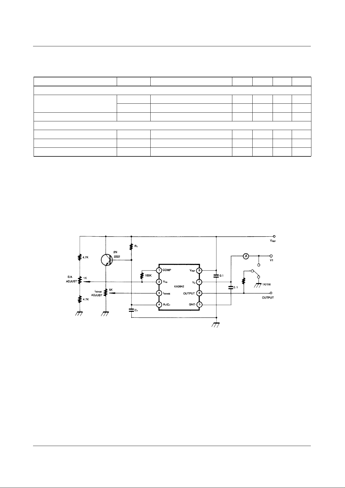
Figure 1. Open Loop Test Circuit
High peak currents associated with capacitive loads necessitate careful grounding techniques Timing and bypass capacitors
should be c onnected close to pin 5 in a single point ground. The transistor and 5KΩ potentiometer are used to sample the
oscillator waveform and apply an adjustable ramp to pin 3.
4
 Loading...