

Fairchild Semiconductor GTLP17T616MTDX, GTLP17T616MTD, GTLP17T616MEAX, GTLP17T616MEA Datasheet
© 2000 Fairchild Semiconductor Corporation DS500327 www.fairchildsemi.com
January 2000
Revised February 2000
GTLP17T616 17-Bit LVTTL/GTLP Bus Tra nsceiver with Buffered Clock
GTLP17T616
17-Bit LVTTL/GTLP Bus Transceiver with Buffered Clock
General Description
The GTLP17T616 is a 17-bit registered bus transceiver
that provides LVTTL to GTLP signal level translation. It
allows for transparent, latched and clocked modes of data
flow and provides a buffered GTLP (CLKOUT) clock output
from the LVTTL CLKAB. The device provides a high spe ed
interface between cards operating at LVTTL logic levels
and a backplane operating at GTLP logic levels. High
speed backplane operation is a direct result of GTLP’s
reduced o utput swing (<1V), reduced input threshold levels
and output edge rate con trol. The edge rate cont rol minimizes bus settling time. GTLP is a Fairchild Semiconductor
derivative of the G unning Transistor logic (GTL) JEDEC
standard JESD8-3.
Fairchild's GTLP has inte rnal ed ge-ra te cont rol and is Process, Voltage, and Temperature (PVT) compensated. Its
function is similar to BTL or GTL but with different output
levels and receiver thresholds. GTLP outpu t LOW level is
typically less than 0. 5V, the output level HIGH is 1.5V and
the receiver threshold is 1.0V.
Features
■ Bidirectional interface between GTLP and LVTTL logic
levels
■ Edge Rate Control to minimize noise on the GTLP port
■ Power up/down high impedance for live insertion
■ External V
REF
pin for receiver threshold adjustability
■ BiCMOS technology for low power dissipation
■ Bushold data input s on A Port eliminates the need for
external pull-up resistors for unused inputs
■ LVTTL compatible Driver and Control inputs
■ Flow-through architecture optimizes PCB layout
■ Open drain on GTLP to support wired-or connection
■ A Port source/sink −24 mA/+24 mA
■ B Port sink capability +50 mA
■ D-type flip-flop, latch and transparent data paths
■ GTLP Buffered CLKAB signal available (CLKOUT)
■ −40°C to +85°C Temperature operation
Ordering Code:
Device also available in Tape and Reel. Specify by appending s uffix let te r “X” to the ordering code.
Order Number Package Number Package Description
GTLP17T616MEA MS56A 56-Lead Shrink Small Outline Package (SSOP), JEDEC MO-118, 0.300” Wide
GTLP17T616MTD MTD56 56-Lead Thin Shrink Small Outline Package (TSSOP), JEDEC MO-153, 6.1mm Wide
www.fairchildsemi.com 2
GTLP17T616
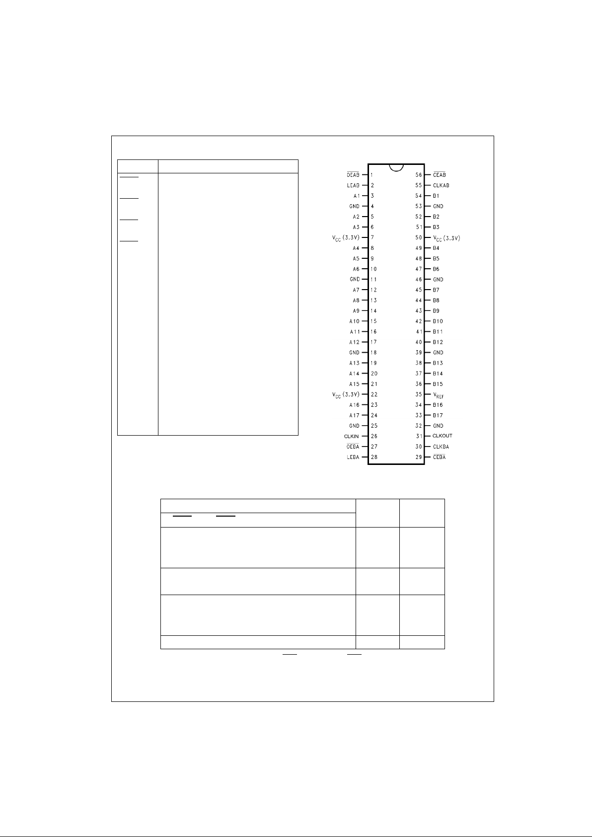
Pin Descriptions Connection Diagram
Truth Table
(Note 1)
Note 1: A-to-B data flo w is sh ow n. B-to-A data flow is similar but uses OEBA, LE BA, CLKBA, and CEBA.
Note 2: Output level before the indicated s t eady state input conditions were established , provided that CLKAB w as H IG H before LEAB went LOW.
Note 3: Output level before the indicated steady-state input conditions were established.
Pin Names Description
OEAB
A-to-B Output Enable
(Active LOW) (LVTTL levels)
OEBA
B-to-A Output Enable
(Active LOW) (LVTTL levels)
CEAB
A-to-B Clock/LE Enable
(Active LOW) (LVTTL levels)
CEBA
B-to-A Clock/LE Enable
(Active LOW) (LVTTL levels)
LEAB A-to-B Latch Enable
(Transparent HIGH) (LVTTL levels)
LEBA B-to-A Latch Enable
(Transparent HIGH) (LVTTL levels)
V
REF
GTLP Input Threshold
Reference Voltage
CLKAB A-to-B Clock (LVTTL levels)
CLKBA B-to-A Clock (LVTTL levels)
A1–A17 A-to-B Data Inputs or
B-to-A 3-STATE Outputs
B1–B17 B-to-A Data Inputs or
A-to-B Open Drain Outputs (GTLP Levels)
CLKIN B-to-A Buffered Clock Output
(LVTTL levels)
CLKOUT GTLP Buffered Clock Input/Output of CLK AB
(GTLP Levels)
Inputs Output
B
Mode
CEAB
OEAB LEAB CLKAB A
X H X XXZ Latched
LLLH or LXB
0
(Note 2) storage
LLLH or LXB
0
(Note 3) of A data
X L H X L L Transparent
XLHXHH
LLL↑ L L Clocked
LLL↑ H H storage
of A data
HLLXXB
0
(Note 3) Clock inhibit
3 www.fairchildsemi.com
GTLP17T616
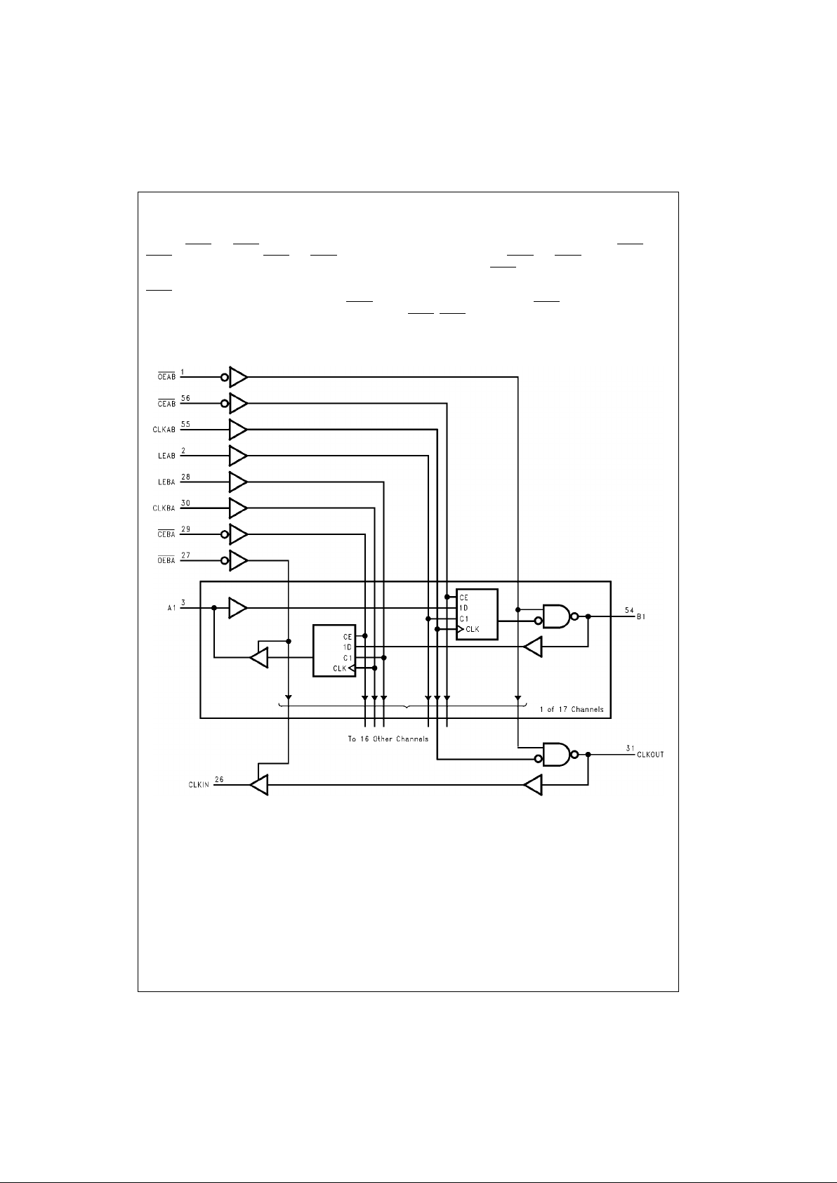
Functional Description
The GTLP17T616 is a 17 bit registered transceiver containing D-type flip-flop, latch and transparent modes of operation for
the data path and a GTLP translation of the CLKAB signal (CLKOUT). Data flow in each direction is controlled by the clock
enables (CEAB
and CEBA), latch enables (LEAB and LEBA), clock (CLKAB and CLKBA) and output enables (OEAB and
OEBA
). The clock enables (CEAB and CEBA) enable all 17 bits. The output enables (OEAB and OEBA) control the 17 bits
of data and the CLKOUT/CLKIN buffered clock path. For A-to-B data flow, when CEAB
is low, the device operates on the
LOW-to-HIGH transition of CLKAB for the flip-flop and on the HIGH-to-LOW transition of LEAB for the latch path. That is, if
CEAB
is LOW and LEAB is LOW the A data is latched regardless as to the state of CLKAB (HIGH or LOW) and if LEAB is
HIGH the device is in transparent mode. When OEAB
is LOW the outputs are active. When OEAB is HIGH the outputs are
high impedance. The data flow of B-to-A is similar except that CEAB
, OEBA, LEBA and CLKBA are used.
Logic Diagram
 Loading...