

Fairchild Semiconductor GTLP16617MTDX, GTLP16617MTD, GTLP16617MEAX, GTLP16617MEA Datasheet
June 1997
Revised October 1998
GTLP16617 17-Bit TTL/GTLP Synchronous Bus Transceiver with Buffered Clock
© 1998 Fairchild Semiconductor Corporation DS500031.prf www.fairchildsemi.com
GTLP16617
17-Bit TTL/GTLP Synchronous Bus Transceiver
with Buffered Clock
General Description
The GTLP16617 is a 17-bit registered synchronous b us
transceiver that provi des TTL t o GTLP signal l evel tr ansl ation. It allows for trans parent, latched and cloc ked modes
of data flow and provides a buffered GTLP (CLKOUT)
clock output from th e TTL CLKAB. Th e device prov ides a
high speed interf ace be tween cards o pe rating at TT L l ogic
levels and a backplane operating at GTLP logic levels.
High speed backplane operation is a direct result of
GTLP’s reduced output swi ng (<1 V), re duced input th reshold levels and output edge rate co ntr ol. Th e ed ge ra te co ntrol minimizes bus settling time. GTLP is a Fairchild
Semiconductor derivati ve of the Gunning Transceiver logic
(GTL) JEDEC standard JESD8-3.
Fairchild’s GTLP has intern al edge -rate cont rol and is process, voltage, and temperature (PVT) compensated. Its
function is similar to BTL and GT L but with different outp ut
levels and receiver threshold. GTLP output LOW level is
typically less than 0. 5V, the output level HIGH is 1.5V and
the receiver threshold is 1.0V.
Features
■ Bidirectional interface between GTLP and TTL logic
levels
■ Edge Rate Control to minimize noise on the GTLP port
■ Power up/down/off high impedance for live insertion.
■ External V
REF
pin for receiver threshold
■ CMOS technology for low power dissipation
■ 5 V tolerant inputs and outputs on the A-Port
■ Bus-hold data inputs on the A-Port eliminates the need
for external pull-up resistors on unused inputs.
■ TTL compatible driver and control inputs
■ Flow through pinout optimizes PCB layout
■ Open drain on GTLP to support wired-or connection
■ A-Port source/sink −32 mA/+32 mA
■ D-type flip-flop, latch and transparent data paths
■ GTLP Buffered CLKA B signal avai lable(CLKOUT)
■ Recommended Operating Temperature −40°C to 85°C
Ordering Code:
Devices also availab le in Tape and Reel. Specify by appending th e s uffix let t er “X” to the ordering cod e.
Order Number Package Number Package Description
GTLP16617MEA MS56A 56-Lead Shrink Small Outline Package (SSOP), JEDEC MO-118 0.300” Wide
GTLP16617MTD MTD56 56-Lead Thin Shrink Small Outline Package (TSSOP), JEDEC MO-153, 6.1mm Wide
www.fairchildsemi.com 2
GTLP16617
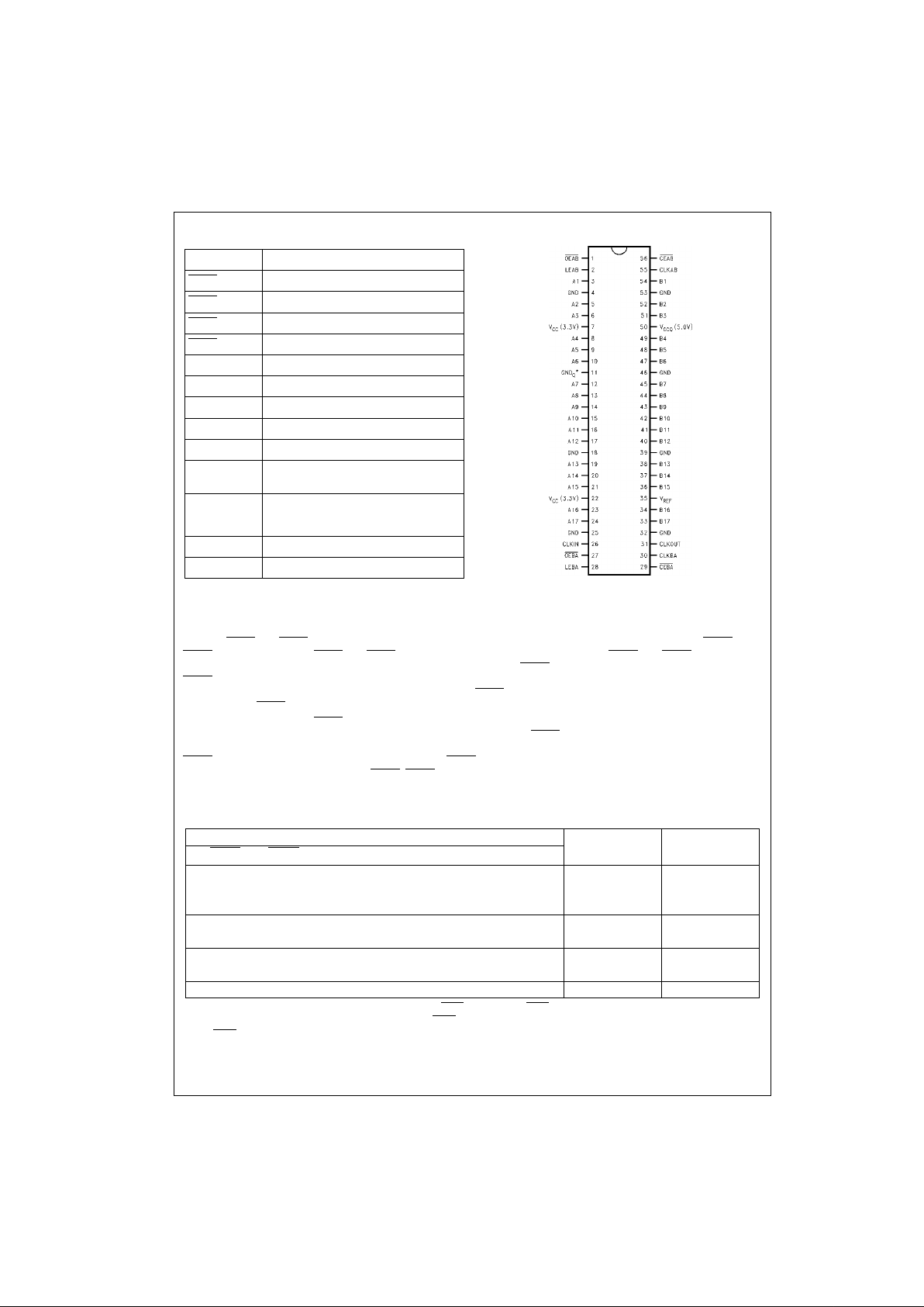
Pin Descriptions Connection Diagram
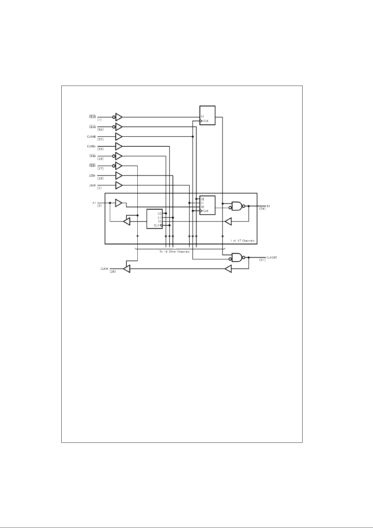
Functional Description
The GTLP16617 is a 17 bit re giste red transce iver co ntaining D-typ e flip-fl op, latch an d transp arent m odes of op eration for
the data path and a GTLP translation of the CLKAB signal (CLKOUT). Data flow in each direction is controlled by the clock
enables (CEAB
and CEBA), latch enables (LEAB and LEBA), clock (CLKAB and CLKBA) and output enables (OEAB and
OEBA
). The clock enables ( CE AB an d CEBA) en able all 17 da ta bits. Th e output en ables (OE AB an d O E BA) control both
the 17 bits of data and the CLKOUT/CLKIN buffered clock paths and the OEAB
is synchronous with the CLKAB signal. The
OEBA
can not be synchronous since we are passing the clock through the device with data and we would need to generate
the CLKBA signal elsew here. It shoul d also be not ed that the OEA B
register is controlled by CLKAB only, and is also not
inhibited by the CEAB
signal.
For A-to-B data flow, when CEAB
is LOW, the device operates o n the LOW-to-HIGH transition of C LKAB for the flip-flop
and on the HIGH-to-LOW transition of LEAB for the latch path. That is, if CEAB
is LOW and LEAB is LOW the A data is
latched regardless as to the state of CLKAB (HIGH or LOW) and if LEAB is HIGH the device is in transparent mode. When
OEAB
is registered LOW the output s are active. Wh en OEAB is r egistered H IGH the outpu ts are HIGH i mpedance. The
data flow of B-to-A is similar except that CEBA
, OEBA, LEBA and CLKBA are used.
Truth Table
(Note 1)
Note 1: A-to-B data flo w is sh ow n. B-to-A data flow is similar but uses OEBA, LEBA, CLKBA, CEBA.
Note 2: LH edge on C LKAB is required when c hanging the input on OEAB
pin.
Note 3: OEAB
met set-up time prior to CLKAB LH transition
Note 4: Output level before the indicated s t eady state input condit ions were established , provided CLKAB was H IG H prior to LEAB going LOW.
Note 5: Output level before the indicated s t eady state input condit ions were established .
Pin Names Description
OEAB
A-to-B Output Enable (Active LOW)
OEBA
B-to-A Output Enable (Active LOW)
CEAB
A-to-B Clock Enable (Active LOW)
CEBA
B-to-A Clock Enable (Active LOW)
LEAB A-to-B Latch Enable (Transparent HIGH)
LEBA B-to-A Latch Enable (Transparent HIGH)
V
REF
GTLP Reference Voltage
CLKAB A-to-B Clock
CLKBA B-to-A Clock
A1-A17 A-to-B Data Inputs or B-to-A 3-STATE
Data Outputs
B1-B17 B-to-A Data Inputs or
A-to-B Open Drain Outputs
CLKIN B-to-A Buffered Clock Output
CLKOUT GTLP Buffered Clock Output of CLKAB
Inputs Output
B
Mode
CEAB
OEAB(Note 2) LEAB CLKAB A
XHX↑ X Z (Note 3) Latched storage of
A data
LLLH or LXB
0
(Note 4)
L L L H or L X (Note 5)
X L H X L L Transparent
XLHXHH
LLL↑ L L Clocked storage of
A data
LLL↑ HH
HLLXXB
0
(Note 5) Clock inhibit
3 www.fairchildsemi.com
GTLP16617
Logic Diagram
 Loading...