


Fairchild Semiconductor GTLP16616MTDX, GTLP16616MTD, GTLP16616MEAX, GTLP16616MEA Datasheet
June 1997
Revised October 1998
GTLP16616 17-Bit TTL/GTLP Bus Transceiver with Buffered Clock
© 1998 Fairchild Semiconductor Corporation DS500017.prf www.fairchildsemi.com
GTLP16616
17-B
it TTL/GTLP Bus Transceiver
with Buffered Clock
General Description
The GTLP16616 i s a 1 7-bit r egist ered bus transc eiver th at
provides TTL to GTLP signal le vel translatio n. It al lows for
transparent, latched and clocked modes of dat a flow and
provides a buffered GTLP (CLKOUT) clock output from the
TTL CLKAB. The device p rovides a high speed interfa ce
between cards operating at TTL logic l evels and a backplane operating at GTLP logic levels. High speed back-
plane operation is a direct resu lt of GTLP’s red uced outp ut
swing (<1V), reduced input threshold levels and output
edge rate control. The edge rate control minimizes bus settling time. GTLP is a Fairchil d Semicondu ctor deriv ative of
the Gunning Transceiver logic (GTL) JEDEC standard
JESD8-3.
Fairchild’s GTLP has inter nal edg e-rate con trol and is process, voltage, and temperature (PVT) compensated. Its
function is similar to BTL and GT L but with different outp ut
levels and receiver threshold. GTLP output LOW level is
typically less than 0. 5V, the output level HIGH is 1.5V and
the receiver threshold is 1.0V.
Features
■ Bidirectional interface between GTLP and TTL logic
levels
■ Edge Rate Control to minimize noise on the GTLP port
■ Power up/down/off high impedance for live insertion
■ External V
REF
pin for receiver threshold
■ CMOS technology for low power dissipation
■ 5 V tolerant inputs and outputs on the A-Port
■ Bus-hold data inputs on the A-Port eliminates the need
for external pull-up resistors on unused inputs.
■ TTL compatible driver and control inputs
■ Flow through pinout optimizes PCB layout
■ Open drain on GTLP to support wired-or connection
■ A-port source/sink −32 mA/+32 mA
■ D-type flip-flop, latch and transparent data paths
■ GTLP Buffered CLKAB signal available (CLKOUT)
■ Recommended Operating Temperature −40°C to 85°C
Ordering Code:
Devices also availab le in Tape and Reel. Specify by appending su ffix let te r “X” to the ordering code .
Order Number Package Number Package Description
GTLP16616MEA MS56A 56-Lead Shrink Small Outline Package (SSOP), JEDEC MO-118 0.300” Wide
GTLP16616MTD MTD56 56-Lead Thin Shrink Small Outline Package (TSSOP), JEDEC MO-153, 6.1mm Wide
www.fairchildsemi.com 2
GTLP16616
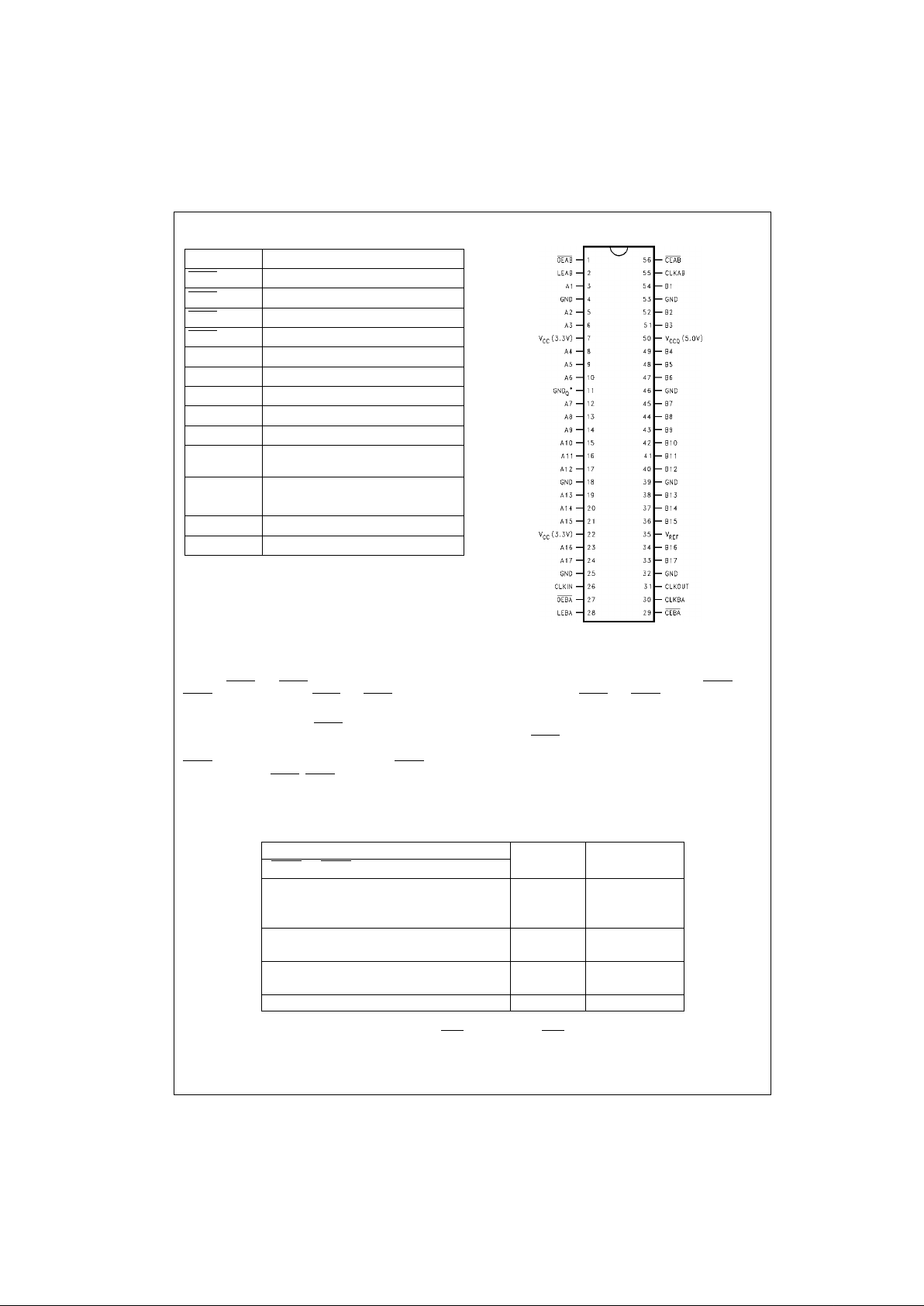
Pin Descriptions Connection Diagram
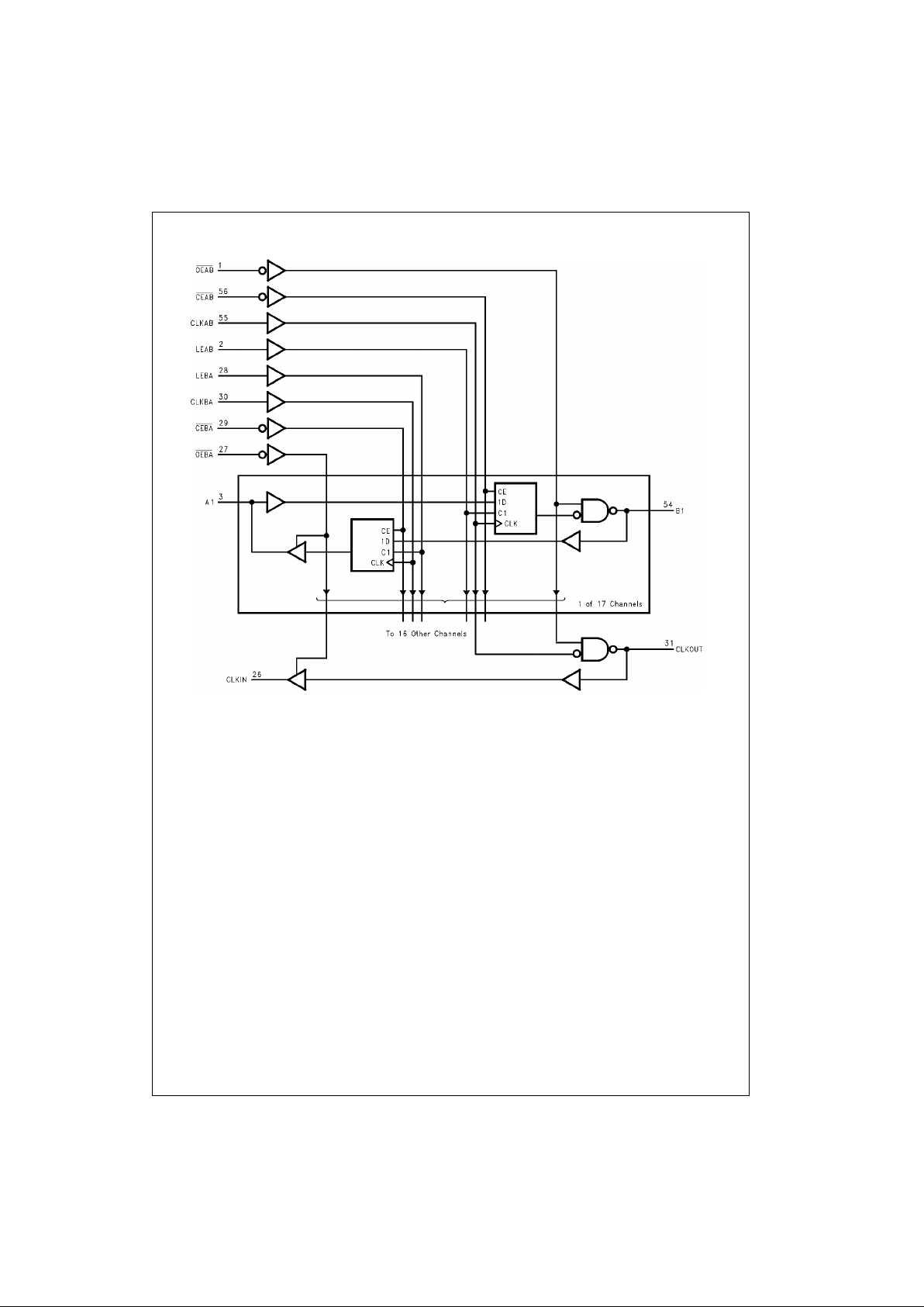
Functional Description
The GTLP16616 is a 17 bit re giste red transce iver co ntaining D-typ e flip-fl op, latch an d transp arent m odes of op eration for
the data path and a GTLP translation of the CLKAB signal (CLKOUT). Data flow in each direction is controlled by the clock
enables (CEAB
and CEBA), latch enables (LEAB and LEBA), clock (CLKAB and CLKBA) and output enables (OEAB and
OEBA
). The clock enables (CEAB and CEBA) enable all 17 bits. The output enables (OEAB and OEBA) control both the 17
bits of data and the CLKOUT/CLKIN buffered clock path.
For A-to-B data flow, when CEAB
is LOW, the device operates o n the LOW-to-HIGH tr ansition of C LKAB for the flip-flop
and on the HIGH-to-LOW transition of LEAB for the latch path. That is, if CEAB
is LOW and LEAB is LOW the A data is
latched regardless as to the state of CLKAB (HIGH or LOW) and if LEAB is HIGH the device is in transparent mode. When
OEAB
is LOW the outputs are active. When OEAB is HIGH the outputs ar e HIGH impedance . The data flow of B-to -A is
similar except that CEBA
, OEBA, LEBA and CLKBA are used.
Truth Table
(Note 1)
Note 1: A-to-B data flo w is sh ow n. B-to-A data flow is similar but uses OEBA, LE BA, CLKBA, and CEBA.
Note 2: Output level before the indicated s t eady-state input conditions were established, provided that CL KAB was HIGH prior to LEAB going LOW.
Note 3: Output level before the indicated steady-state input conditions were established.
Pin Names Description
OEAB
A-to-B Output Enable (Active LOW)
OEBA
B-to-A Output Enable (Active LOW)
CEAB
A-to-B Clock Enable (Active LOW)
CEBA
B-to-A Clock Enable (Active LOW)
LEAB A-to-B Latch Enable (Transparent HIGH)
LEBA B-to-A Latch Enable (Transparent HIGH)
V
REF
GTLP Reference Voltage
CLKAB A-to-B Clock
CLKBA B-to-A Clock
A1-A17 A-to-B Data Inputs or B-to-A 3-STATE
Outputs
B1-B17 B-to-A Data Inputs or
A-to-B Open Drain Outputs
CLKIN B-to-A Buffered Clock Output
CLKOUT GTLP Buffered Clock Output of CLKAB
Inputs Output
B
Mode
CEAB
OEAB LEAB CLKAB A
X H X X X Z Latched
LLLH or LXB
0
(Note 2) storage
LLLH or LXB
0
(Note 3) of A data
X L H X L L Transparent
XLHXH H
LLL↑ L L Clocked storage
LLL↑ H H of A data
HLLXXB
0
(Note 3) Clock inhibit
3 www.fairchildsemi.com
GTLP16616
Logic Diagram