

Fairchild Semiconductor GTLP16612MTDX, GTLP16612MTD, GTLP16612MEAX, GTLP16612MEA Datasheet
March 1995
Revised October 1998
GTLP16612 CMOS 18-Bit TTL/GTLP Universal Bus Transceiver
© 1998 Fairchild Semiconductor Corporation DS012390.prf www.fairchildsemi.com
GTLP16612
CMOS 18-Bit TTL/GTLP Universal Bus Transceiver
General Description
The GTLP16612 is an 18-bit universal bus transceiver
which provides TTL to GTLP signal level translation. The
device is designed to provide a high speed interface
between cards operating at TTL logic l evels and a backplane operating at GTLP logic levels. High speed backplane operation i s a di r ect re sult of G TL P’s redu ced output
swing (<1V), reduced input threshold levels and output
edge rate control which minimizes signal settling times.
GTLP is a Fairchild Semiconduct or derivative of the Gunning Transceiver Logic (GTL) JEDEC standard JESD8-3.
Fairchild’s GTLP has inte rnal edge- rate control and is Pr ocess, Voltage, and Temperature (PVT) compensated. Its
function is similar to B TL or GTL but with different driver
output levels and receiver threshold. GTLP output low voltage is typically less than 0.5V, the output high is 1 .5V and
the receiver threshold is 1.0V.
Features
■ Bidirectional interface between GTLP and TTL logic
levels
■ Designed with Edge Rate Control Circuit to reduce
output noise
■ V
REF
pin provides extern al supply re ference volta ge for
receiver threshold
■ Submicron Core CMOS technology for low power
dissipation
■ Special PVT Compensatio n circuitry to provide consistent performance over variations of process, supply
voltage and temperature
■ 5V tolerant inputs and outputs on A-Port
■ Bus-Hold data inputs on A-P o rt to elimi n ate the n eed for
external pull-up resistors for unused inputs
■ Power up/down high impedance
■ TTL compatible Driver and Control inputs
■ A-Port outputs source/sink −32 mA/+32 mA
■ Flow-through architecture optimizes PCB layout
■ Open drain on GTLP to support wired-or connection
Ordering Code:
Device also available in Tape and Reel. Specify by appending s uffix let te r “X” to the ordering code .
Order Number Package Number Package Description
GTLP16612MEA MS56A 56-Lead Shrink Small Outline Package (SSOP), JEDEC MO-118 0.300” Wide
GTLP16612MTD MTD56 56-Lead Thin Shrink Small Outline Package (TSSOP), JEDEC MO-153, 6.1mm Wide
www.fairchildsemi.com 2
GTLP16612
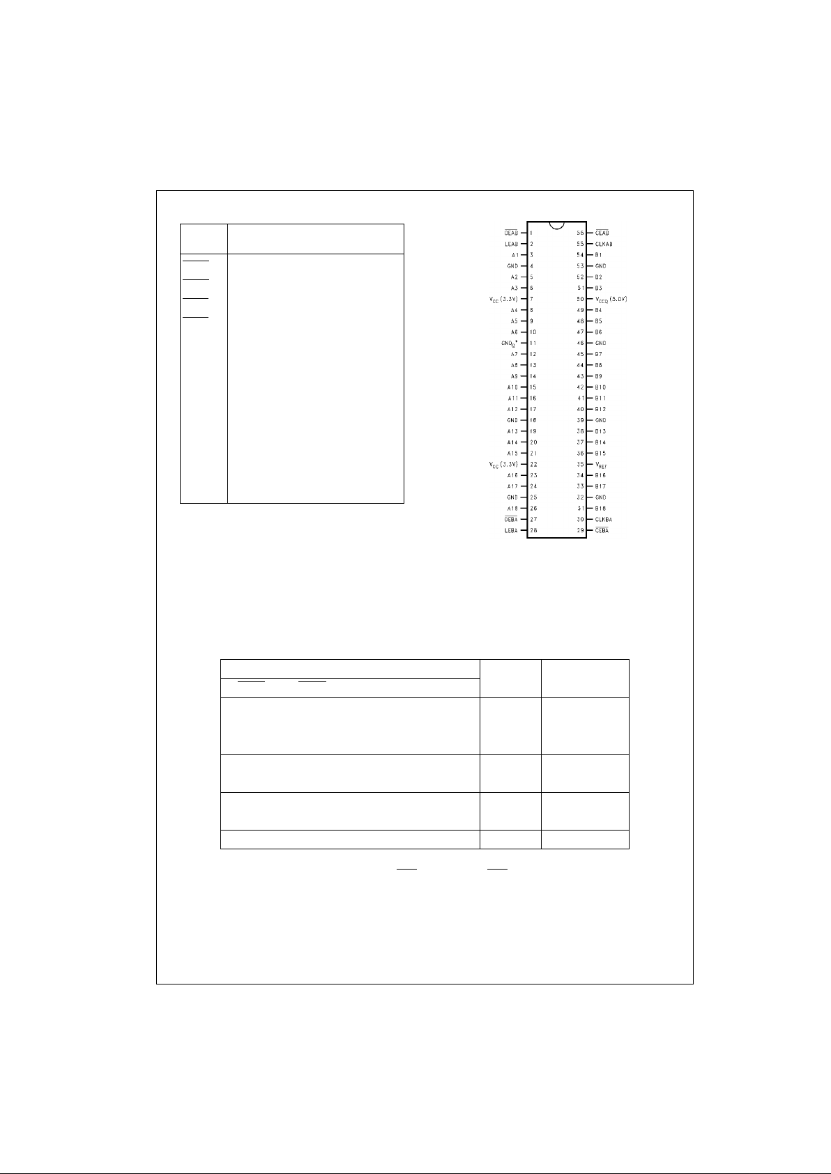
Pin Descriptions Connection Diagram
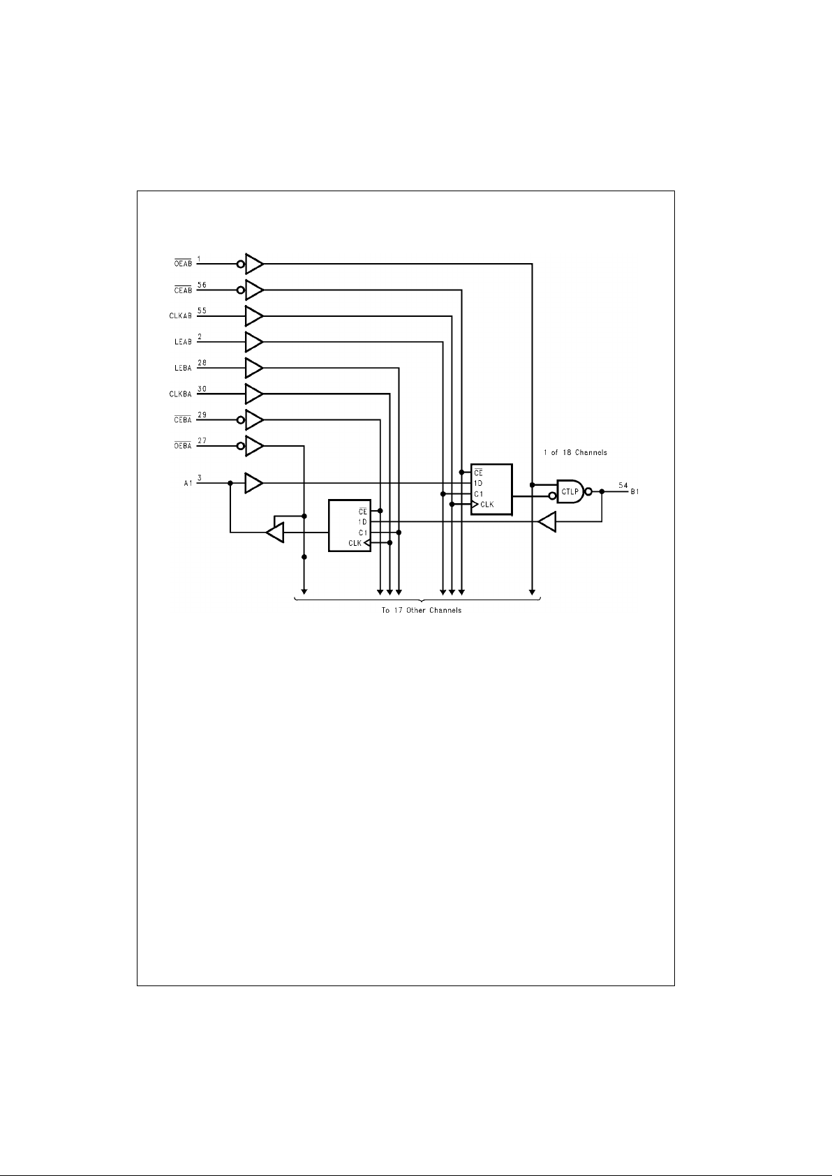
Functional Description
The GTLP16612 com bines a univers al transceiver f unction with a T TL to GTLP transl ation. The A-P ort and control pins
operate at LVTTL or 5V TTL levels while the B-Port operates at GTLP levels. The transceiver logic includes D-type latch es
and D-type flip-flops to allow data flow in transparent, latched and clock mode.
The functional operation is described in the truth table below.
Truth Table
(Note 1)
Note 1: A-to-B data flo w is sh ow n. B-to-A data flow is similar but uses OEBA, LEBA, CLKBA, and CEBA.
Note 2: Output level before the indicated s t eady-state input conditions were establis hed, provided that CL KAB was high before LE AB went low.
Note 3: Output level before the indicated steady-state input conditions were established.
Pin
Names
Description
OEAB
A-to-B Output Enable (Active LOW)
OEBA
B-to-A Output Enable (Active LOW)
CEAB
A-to-B Clock Enable (Active LOW)
CEBA
B-to-A Clock Enable (Active LOW)
LEAB A-to-B Latch Enable (Transparent HIGH)
LEBA B-to-A Latch Enable (Transparent HIGH)
CLKAB A-to-B Clock Pulse
CLKBA B-to-A Clock Pulse
V
REF
GTLP Input Reference Voltage
A1–A18 A-to-B TTL Data Inputs or
B-to-A 3-STA TE Outputs
B1–B18 B-to-A GTLP Data Inputs or
A-to-B Open Drain Outputs
Inputs Output
B
Mode
CEAB
OEAB LEAB CL KAB A
X H X X X Z Latched
LLLHXB
0
(Note 2) storage
LLLLXB
0
(Note 3) of A data
X L H X L L Transparent
XLHXHH
LLL↑ L L Clocked storage
LLL↑ H H of A data
HLLXXB
0
(Note 3) Clock inhibit
3 www.fairchildsemi.com
GTLP16612
Logic Diagram
 Loading...