Fairchild Semiconductor GTLP10B320 Datasheet

GTLP10B320
10-Bit LVTTL/GTLP Transceiver
with Split LVTTL Port and Feedback Path
GTLP10B320 10-Bit LVTTL/GTLP Transceiver with Split LVTTL Port and Feedback Path
May 2001
Revised May 2001
General Description
The GTLP10B320 is a 10-bit Universal bus driver and
receiver, with separate LVTTL inputs and outputs and a
feedback path for diagnostics, that provides LVTTL to
GTLP signal level t ranslatio n. H igh spe ed bac kplan e operation is a direct result of GTLP’s reduced output swing
(
<1V), reduced input thresh old le vels a nd outp ut edg e rate
control. The edge rate c ontrol mi nimizes b us settl ing time.
GTLP is a Fairchild Semiconductor derivative of the
Gunning Transistor logic (GTL) JEDEC stan dard JESD8-3.
Fairchild’s GTLP has intern al edge -rate cont rol and i s process, voltage and temperature (PVT) compensated. Its
function is similar to BTL and GT L but with different o utput
levels and receiver threshold. GTLP out put l ow level i s typically less than 0.5V, the output level high is 1.5V and the
receiver threshold is 1.0V.
Features
■ Bidirectional interface between GTLP and LVTTL logic
levels
■ Variable edge rate control pin to select desired edge rate
on GTLP port (V
pin provides extern al supply re ference volta ge for
■ V
REF
receiver threshold adjustibility
■ Split LVTTL inputs and outputs
■ Special PVT compensation circui try to provide consis-
tent performance over var iatio ns of pr ocess, supply voltage and temperature
■ A feedback path for control and diagnostics monitoring
■ TTL compatible driver and control inputs
■ Designed using Fairchild advanced BiCMOS technology
■ Bushold data inputs on A port to e liminate the need for
external pull-up resistors for unused inputs
■ Power up/down and power off high impedance for live
insertion
■ Open drain on GTLP to support wired-or connection
■ Flow through pinout optimizes PCB layout
■ A Port source/sink
■ B Port sink
+50mA
)
ERC
−24mA/+24mA
Ordering Code:
Order Number Package Number Package Description
GTLP10B320MTD MTD56 56-Lead Thin Shrink Small Outline Package (TSSOP), JEDEC MO-153, 6.1mm Wide
Device is also available in Tape and Reel. Specify by append ing the suffix letter “X” to the ordering code.
© 2001 Fairchild Semiconductor Corporation DS500483 www.fairchildsemi.com

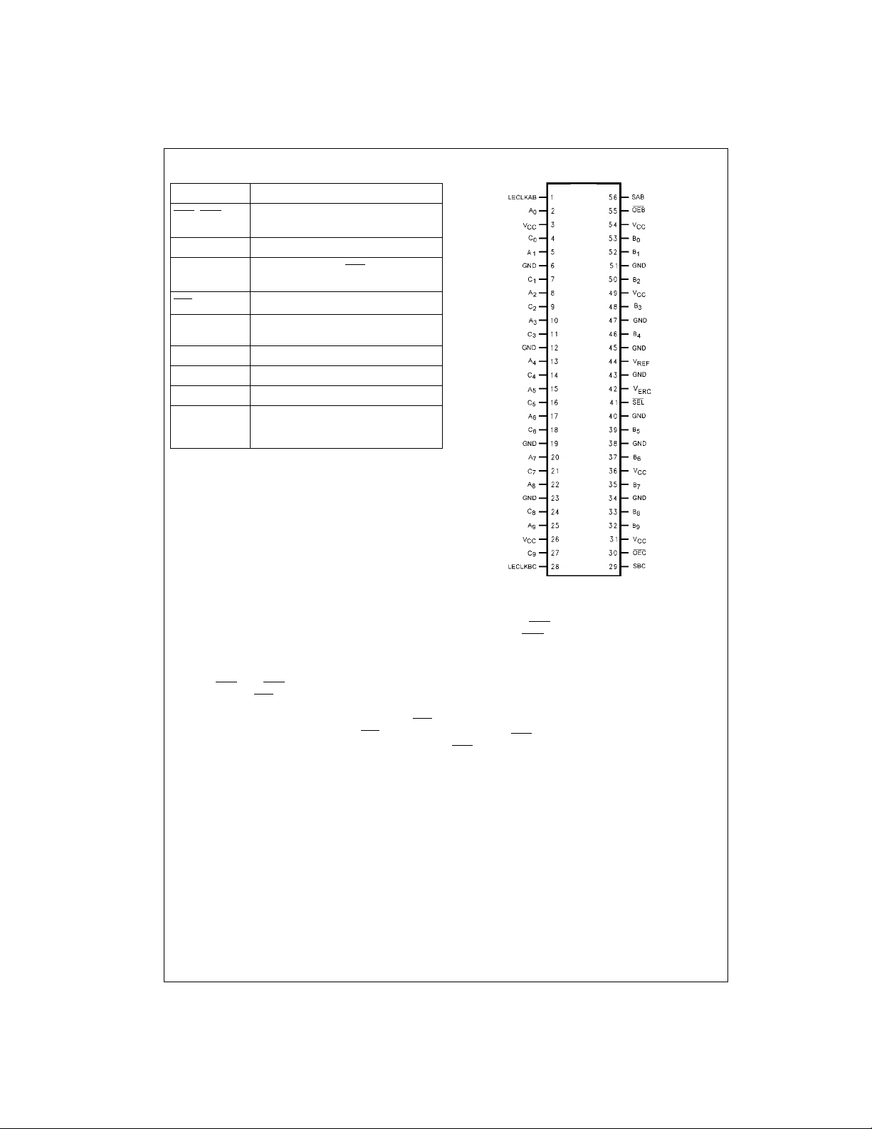
Pin Descriptions Connection Diagram
Pin Names Description
, OEC B Port, C Port Output Enable
OEB
GTLP10B320
, GND, V
V
CC
LECLKAB,
LECLKBC
SEL
SAB, SBC Selects Register or Latch/Transparent
B
0-B9
A
0-A9
C
0-C9
V
ERC
respectively (Active LOW)
Device Supplies
REF
A-to-B, B-to-C Latch CLK
(Transparent Active HIGH)
Selects Internal Feedback Path
Path for A-to-B and B-to-C respectively
B Port GTLP I/O
A Port LV TTL Inputs
C Port LVTTL Outputs
Edge Rate Control Pin
= Slow Edge Rate)
(GND
= Fast Edge Rate)
(V
CC
respectively
Functional Description
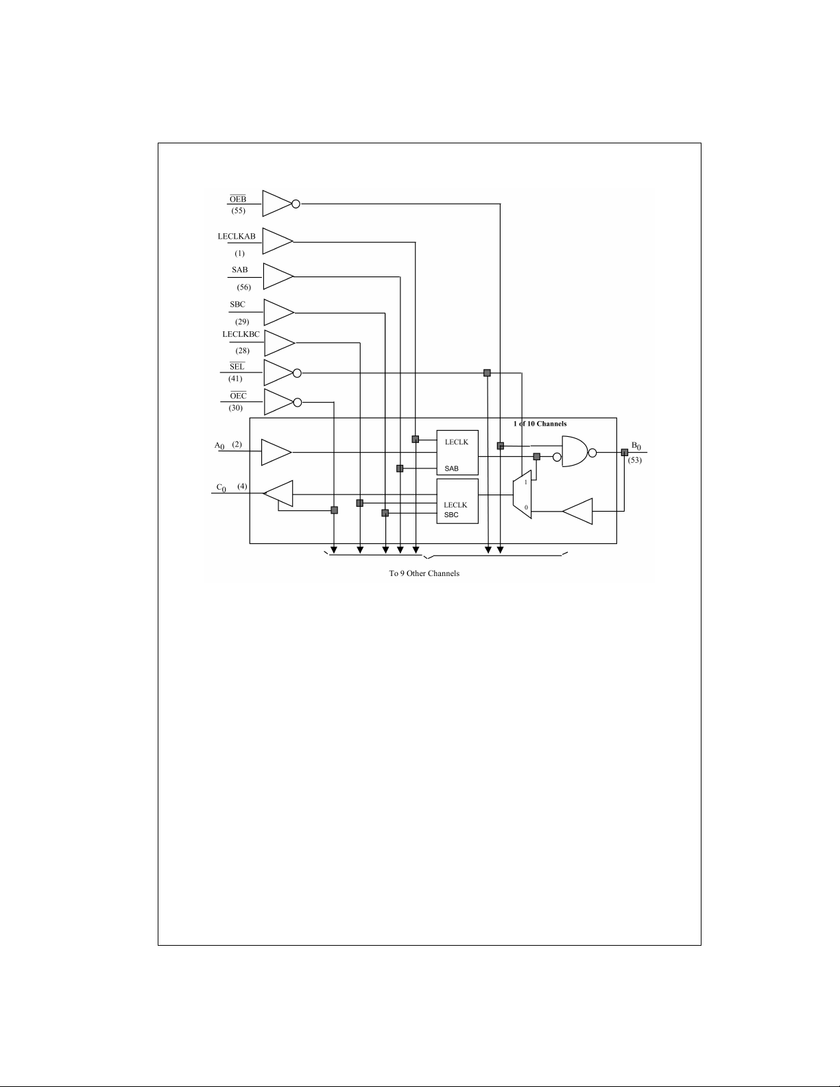
The GTLP10B320 is a 10-bit Univ ersal drive r and receive r
containing D-Type flip-flop, latch, and transparent modes of
operation for the data paths. In addition there is an internal
feedback pat h tha t ca n be used for di agno st ic mon it orin g or
caching schemes. Data flow i n each dir ection is controlled
by the clock signals (LECLKAB and LECLKBC) an d o utp ut
enables (OEB
controlled by t he SEL
Port A to Port C wit hout requiring data to be ou tput to the
backplane. Th e in t er nal f ee dba c k pat h i s s ele c t ed wi th S EL
LOW and the B Port pin is selected w ith SEL HIGH. The
data paths can also be configured for latch/transparent or
register mode for each direction with the SAB and SBC
www.fairchildsemi.com 2
and OEC). The internal feedback path is
pin and allows data transfer from
pins. Data polarity is non-inverting wi th the GTLP outputs
enabled via the OEB
enabled via the OEC
For A-to-B data flow the device is configured in to a latch/
transparent or register mode by pin SAB. If SAB is LOW
then the register mode is sel e cted and th e de vice op era tes
on the LOW-to-HIGH transition of LECLKAB. If SAB is
HIGH then the latch/transpa rent configuration is selected
and a HIGH-to-LOW transit ion of LECLKAB sto res data in
the latch. If LECLKAB is HIGH the device is in transparent
mode. When OEB
OEB
is HIGH the outputs are high impedance.
pin and the LVTTL outputs being
pin.
is LOW the outputs are active and when

Functional Tables
I/O Path: SEL = 1 (External Feedback Path) (Note 2)
Inputs Outputs
OEB OEC SAB SBC LECLKAB LECLKBC Mode
(AB)
010X ↑ XRegisterLX L
010X
↑ XRegisterHX H
010X L X Register L XB
010X L X Register H XB
011X
↓ X Latch L X L
011X H X Buffer L X L
011X
↓ X Latch H X H
011X H X Buffer H X H
1 1 X X X X High Impedance X X Z
Note 1: Output level before the indicated steady stat e input conditions were es t ablished.
Note 2: The data flow of B-to-C is similar except that OEC
Internal Feedback Path: SEL
= 0 (Internal Feedback Path) (Note 3)
, SBC and LECLK BC are used.
Inputs Outputs
OEB OEC SAB SBC LECLKAB LECLKBC Mode
(AB/BC)
0000 ↑↑Register/Register L L L
0000
0000 L
0000
0000
↑↑Register/Register H H H
↑ Register/Register X B
↑ L Register/Register L L B
↑ L Register/Register H H B
0000 L LRegister/RegisterXB
0001
0001
0001
0001
0001 L
↑↓Register/Latch L L L
↑ H Register/Buffer L L L
↑↓Register/Latch H H H
↑ H Register/Buffer H H H
↓ Register/Latch X B
0001 L HRegister/BufferXB
0001 L LRegister/LatchXB
0010
0010
0010
0010
0010 H
0010 H
↓↑Latch/Register L L L
↓↑Latch/Register H H H
↓ L Latch/Register L L B
↓ L Latch/Register H H B
↑ Buffer/Register L L L
↑ Buffer/Register H H H
0010 L LLatch/RegisterXB
0011
0011
↓↓Latch/Latch L L L
↓↓Latch/Latch H H H
0011 H HBuffer/BufferL L L
0011 H HBuffer/BufferH H H
1 1 X X X X High Impedance X Z Z
A
n
A
n
(Note 4) B0 (Note 4)
0
(Note 4) B0 (Note 4)
0
(Note 4) B0 (Note 4)
0
(Note 4) B0 (Note 4)
0
(Note 4) B0 (Note 4)
0
(Note 4) B0 (Note 4)
0
C
n
B
n
B
n
(Note 1)
0
(Note 1)
0
C
n
(Note 4)
0
(Note 4)
0
(Note 4)
0
(Note 4)
0
GTLP10B320
Note 3: Function identical for SEL
Note 4: Output level before the indicated steady stat e input conditions were es t ablished.
= 1 if timing requirem ents for propagatio n delay to output and set -up to LECLKBC are m et at B Port.
3 www.fairchildsemi.com

Logic Diagram
GTLP10B320
www.fairchildsemi.com 4
 Loading...