

Fairchild Semiconductor DM74LS377WMX, DM74LS377WM, DM74LS377N Datasheet
© 2000 Fairchild Semiconductor Corporation DS009831 www.fairchildsemi.com
October 1988
Revised March 2000
DM74LS377 Octal D-Type Flip-Flop with Common Enable and Clock
DM74LS377
Octal D-Type Flip-Flop with Common Enable and Clock
General Description
The DM74LS377 is an 8-bit regist er built using advanced
low power Schottky technolo gy. This register consists of
eight D-type flip-flops with a buffere d common clock a nd a
buffered common input enable. T he device is packaged in
the space-saving (0.3 inch row spacing) 20-pin package.
Features
■ 8-bit high speed parallel registers
■ Positive edge-triggered D-type flip-flops
■ Fully buffered common clock and enable inputs
Ordering Code:
Devices also availab le in Tape and Reel. Specify by appending th e s uffix let t er “X” to the ordering code.
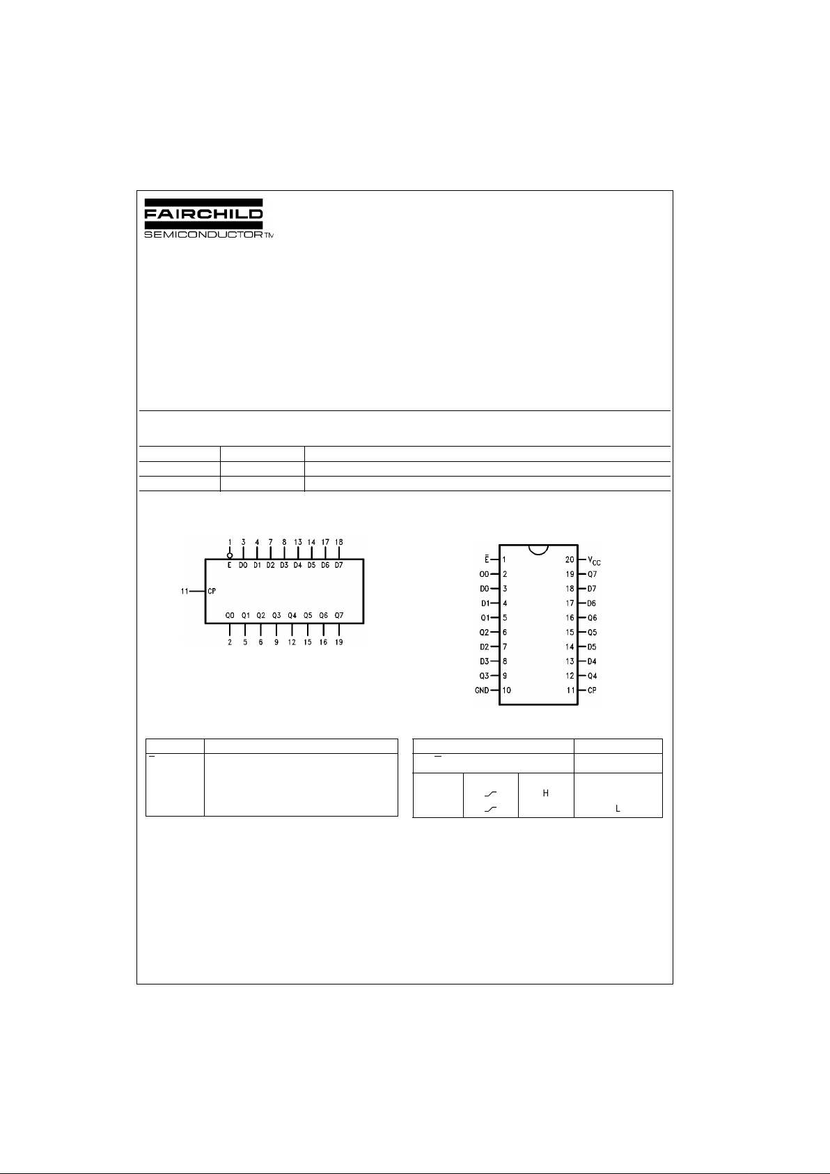
Logic Symbol
VCC = Pin 20
GND = Pin 10
Pin Descriptions
Connection Diagram
Truth Table
H = HIGH Voltage Level
L = LOW Voltage Level
X = Immaterial
Order Number Package Number Package Description
DM74LS377WM M20B 20-Lead Small Outline Integrated Circuit (SOIC), JEDEC MS-013, 0.300 Wide
DM74LS377N N20A 20-Lead Plastic Dual-In-Line Package (PDIP), JEDEC MS-001, 0.300 Wide
Pin Names Description
E
Enable Input (Active LOW)
D0–D7 Data Inputs
CP Clock Pulse Input (Active Rising Edge)
Q0–Q7 Flip-Flop Outputs
Inputs Output
E
CP
D
n
Q
n
H X X No Change
L
HH
L
LL

www.fairchildsemi.com 2
DM74LS377
Functional Description
The DM74LS377 co nsists of ei ght edge -triggered D flip-flo ps with in dividual D inputs and Q outputs. The Clock ( CP) and
Enable input (E
) are common to all flip-flops.
When E
is LOW, new data is entered into the register on the next LOW-to-HIGH transition of CP. When E is HIGH, the reg-
ister will retain the present data independent of the CP.
Logic Diagram
 Loading...