© 2000 Fairchild Semiconductor Corporation DS009827 www.fairchildsemi.com
October 1988
Revised March 2000
DM74LS299 8-Input Universal Shift/Storage Register with Common Parallel I/O Pins
DM74LS299
8-Input Universal Shift/Storage Register with
Common Parallel I/O Pins
General Description
The DM74LS299 is an 8-b it univ ersal shift/stor age r egist er
with 3-STATE outputs. Four modes of opera tion are possi ble: hold (store), shift left, shift right and load data. The parallel load inputs and flip-flop outputs are multiplexed to
reduce the total number of package pins. Separate outputs
are provided for flip-flops Q0 and Q7 to allow easy cascading. A separate active LOW Master Reset is used to reset
the register.
Features
■ Common I/O for reduced pin count
■ Four operation modes: shift left, shift right, load and
store
■ Separate shift right serial input and shift left se rial input
for easy cascading
■ 3-STATE outputs for bus oriented applications
Ordering Code:
Devices also availab le in Tape and Reel. Specify by appending th e s uffix let t er “X” to the ordering code.
Logic Symbol
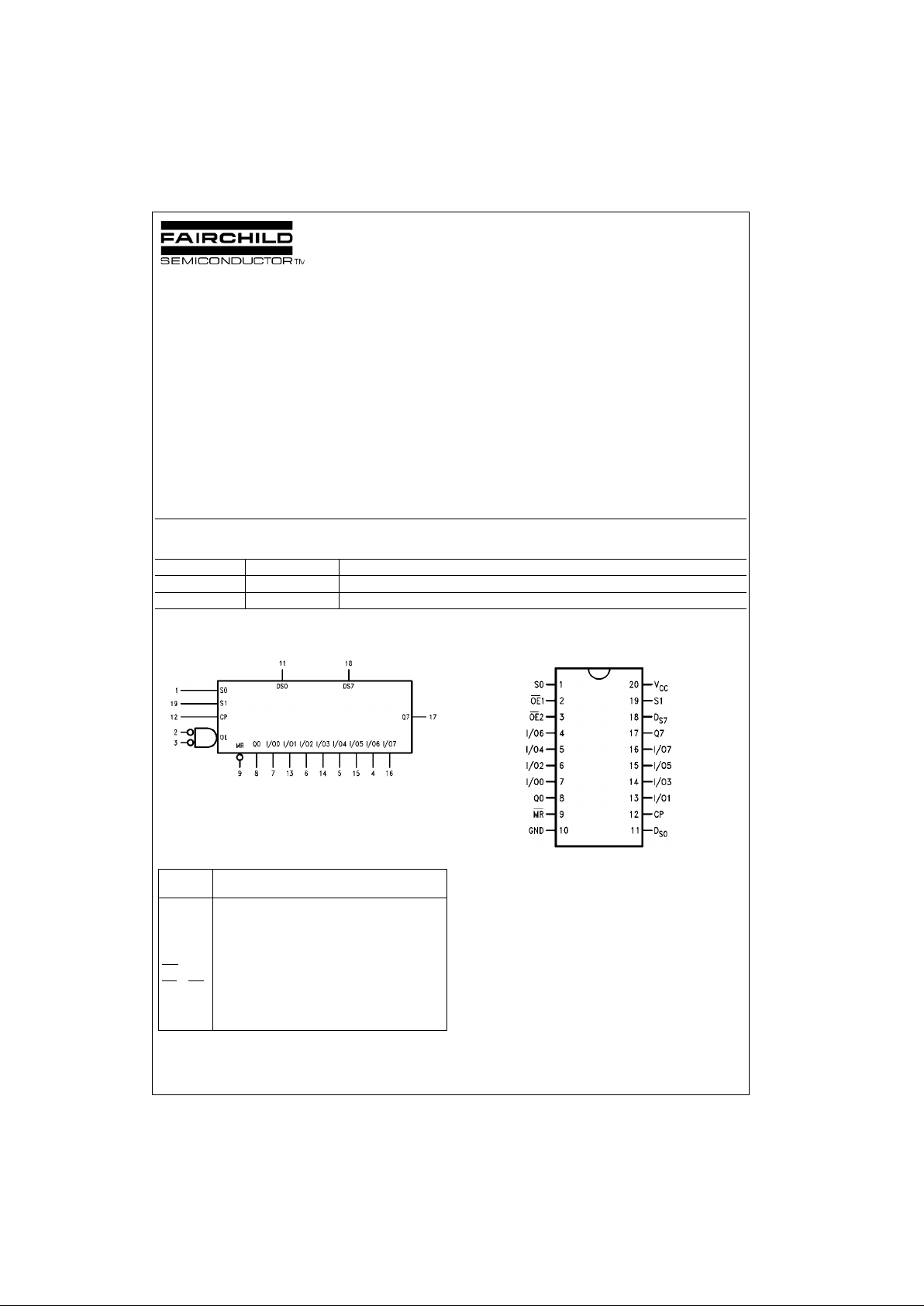
VCC = Pin 20
GND = Pin 10
Pin Descriptions
Connection Diagram
Order Number Package Number Package Description
DM74LS299WM M20B 20-Lead Small Outline Integrated Circuit (SOIC), JEDEC MS-013, 0.300 Wide
DM74LS299N N20A 20-Lead Plastic Dual-In-Line Package (PDIP), JEDEC MS-001, 0.300 Wide
Pin
Names
Description
CP Clock Pulse Input (Active Rising Edge)
D
S0
Serial Data Input for Right Shift
D
S7
Serial Data Input for Left Shift
S0, S1 Mode Select Inputs
MR
Asynchronous Master Reset Input (Active LOW)
OE
1, OE2 3-STATE Output Enable Inputs (Active LOW)
I/O0–I/O7 Parallel Data Inputs or 3-STATE Parallel Outputs
Q0–Q7 Serial Outputs

www.fairchildsemi.com 2
DM74LS299
Functional Description
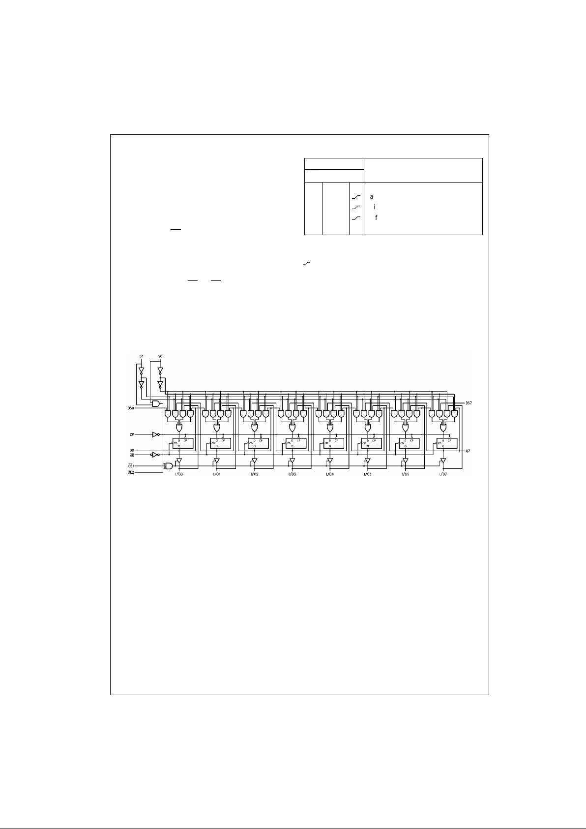
The DM74LS299 contains eight edge- tri g ge red D - type f lip flops and the interstage l ogic necessary to perform synchronous shift left, shift righ t, parallel loa d and hold operations. The type of operation is determi ned by the S0 and
S1, as shown in the Mode Select Table. All flip-flop outputs
are brought out through 3-STATE buffers to separat e I/O
pins that also serve as data inputs in the parallel load
mode. Q0 and Q7 are also brou ght out on other pins for
expansion in serial shifting of longer words.
A LOW signal on MR
overrides the Sele ct and CP inputs
and resets the flip-flops. All other state changes are initiated by the rising edge of the clock. Inputs can change
when the clock is in either st ate prov ided only that th e recommended setup and hold times, relative to the rising edge
of CP, are observed.
A HIGH signal on either OE
1 or OE2 disables the 3-STATE
buffers and puts the I/O pins in the high impedance stat e.
In this condition the sh ift, hold, load and reset operatio ns
can still occur. The 3-STATE buffers are also disabled by
HIGH signals on both S0 and S1 in preparation for a parallel load operation.
Mode Select Table
H = HIGH Voltage Level
L = LOW Voltage Level
X = Immaterial
= LOW-to-HIGH Clock (CP) Transition
Logic Diagram
Inputs
Response
MR
S1 S0 CP
LXXXAsynchronous Reset; Q0–Q7 = LOW
HHH
Parallel Load; I/On→Q
n
HLHShift Right; DS0→Q0, Q0→Q1, etc.
HHL
Shift Left; DS7→Q7, Q7→Q6, etc.
H L L X Hold
 Loading...