Fairchild Semiconductor DM74LS161AM, DM74LS161ACW, DM74LS161AN, DM74LS161AMX Datasheet

© 2000 Fairchild Semiconductor Corporation DS006397 www.fairchildsemi.com
August 1986
Revised April 2000
DM74LS161A • DM74LS163A Synchronous 4-Bit Binary Counters
DM74LS161A • DM74LS163A
Synchronous 4-Bit Binary Counters
General Description
These synchronous, presetta ble counters fe ature an internal carry look-ahead for a ppli ca tion i n high -sp eed co unt i ng
designs. The DM74LS161A and DM74LS163A are 4-bit
binary counters. The carry output is decoded by means of
a NOR gate, thus preventing spikes during the normal
counting mode of operation. Synchronous operation is provided by having all flip-flops clocked simultaneously so that
the outputs change coincident with each other when so
instructed by the count-enabl e inputs and internal gating.
This mode of operation eliminates the output counting
spikes which are normally associated with asynchronous
(ripple clock) counters. A buffer ed clock input triggers t he
four flip-flops on the rising (positive-going) edge of the
clock input waveform.
These counters are fully programmable; that is, the outputs
may be preset to either level. As presetting is synchronous,
setting up a low level at the load in pu t disab les th e co unter
and causes the outputs to a gree with the setup dat a after
the next clock pulse, re gardle ss of the le vels of th e ena ble
input. The clear function for the DM74LS161A is asynchronous; and a low level at the clear input se ts all four of t he
flip-flop outputs LOW, regardless of the levels of clock,
load, or enable inputs. The clear function for the
DM74LS163A is synchro nous; and a low leve l at the cle ar
inputs sets all four of the flip-flo p outputs LOW after the
next clock pulse, regardless of the levels of the enable
inputs. This synchronou s clear allows the count length to
be modified easily, as decoding the maximum count
desired can be accomplished with one external NAND
gate. The gate output i s connected to the clear input to
synchronously clear the counter to all low outputs.
The carry look-ahead circuitry provides for cascading
counters for n-bit synchro nous applications without additional gating. Instrumental in accomplishing this function
are two count-enable inputs and a ripple carry output.
Both count-enable inputs (P and T) must be HIGH to count,
and input T is fed forward to e nab l e th e rip ple ca rr y out put.
The ripple carry output thus enabled will produce a highlevel output pulse w ith a duration approxim ately equal to
the high-level portion of the Q
A
output. This high-level over-
flow ripple carry pu lse can be used to enable successive
cascaded stages. HIGH-to-LOW level transitions at the
enable P or T inpu ts may occur, regardless of the logic
level of the clock.
These counters fe ature a fully independent clock ci rcuit.
Changes made to control inputs (enable P or T or load) that
will modify the operating mode have no effect until clocking
occurs. The function of the cou nter (whether en abled, disabled, loading, or counting ) will be dictated solely by the
conditions meeting th e stable set-up and hold times.
Features
■ Synchronously programmable
■ Internal look-ahead for fast counting
■ Carry out put for n-bit cascading
■ Synchronous counting
■ Load control line
■ Diode-clamped inputs
■ Typical propagation time, clock to Q output 14 ns
■ Typical clock frequency 32 MHz
■ Typical power dissipation 93 mW
Ordering Code:
Devices also availab le in Tape and Reel. Specify by appending th e s uffix let t er “X” to the ordering code.
Order Number Package Number Package Description
DM74LS161AM M16A 16-Lead Small Outline Integrated Circuit (SOIC), JEDEC MS-012, 0.150 Narrow
DM74LS161AN N16E 16-Lead Plastic Dual-In-Line Package (PDIP), JEDEC MS-001, 0.300 Wide
DM74LS163AM M16A 16-Lead Small Outline Integrated Circuit (SOIC), JEDEC MS-012, 0.150 Narrow
DM74LS163AN N16E 16-Lead Plastic Dual-In-Line Package (PDIP), JEDEC MS-001, 0.300 Wide

www.fairchildsemi.com 2
DM74LS161A • DM74LS163A
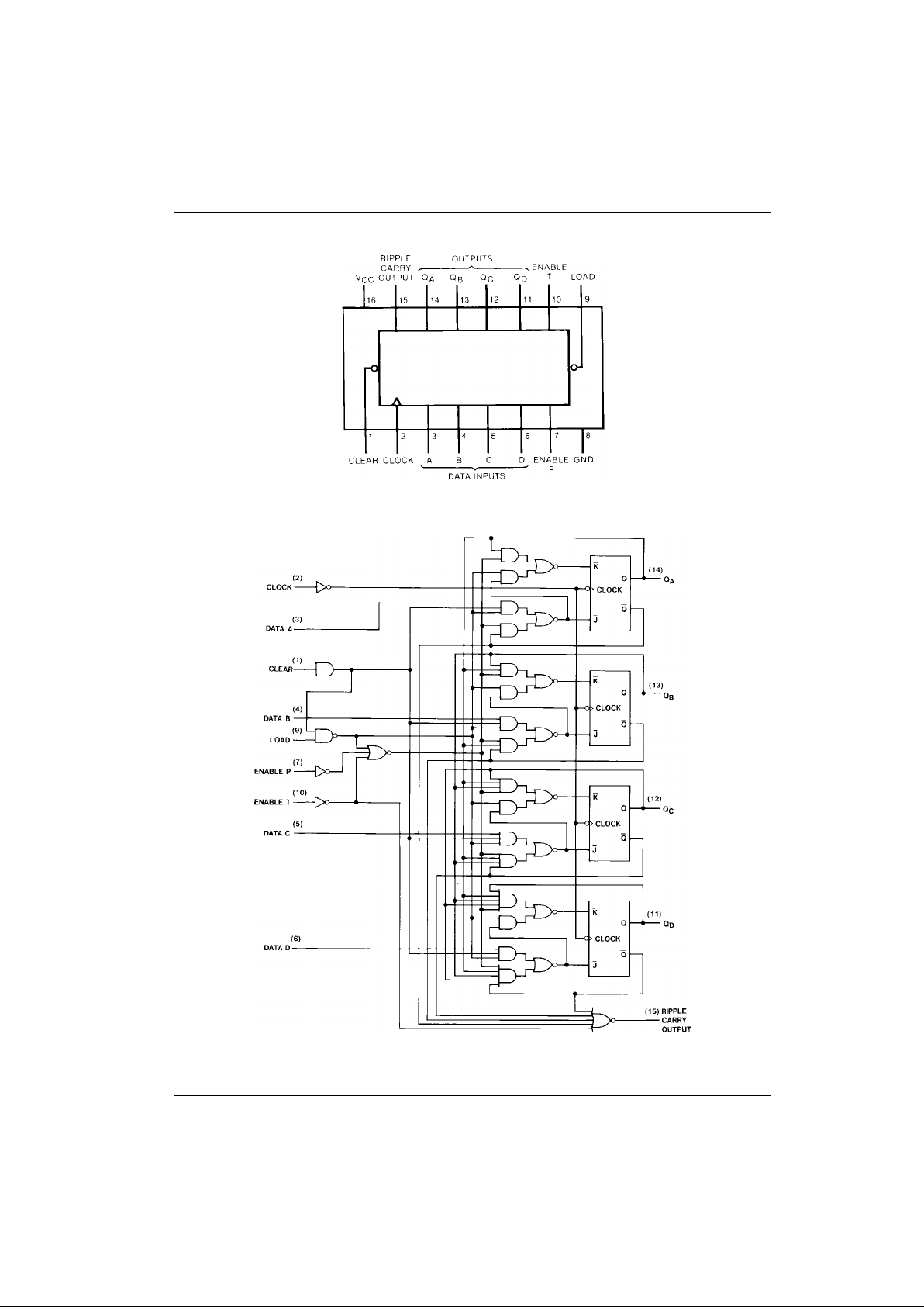
Connection Diagram
Logic Diagram
DM74LS163A
The DM74LS161A is similar, however, the clear buffer is conn ec t ed directly to the flip-flops .

3 www.fairchildsemi.com
DM74LS161A • DM74LS163A
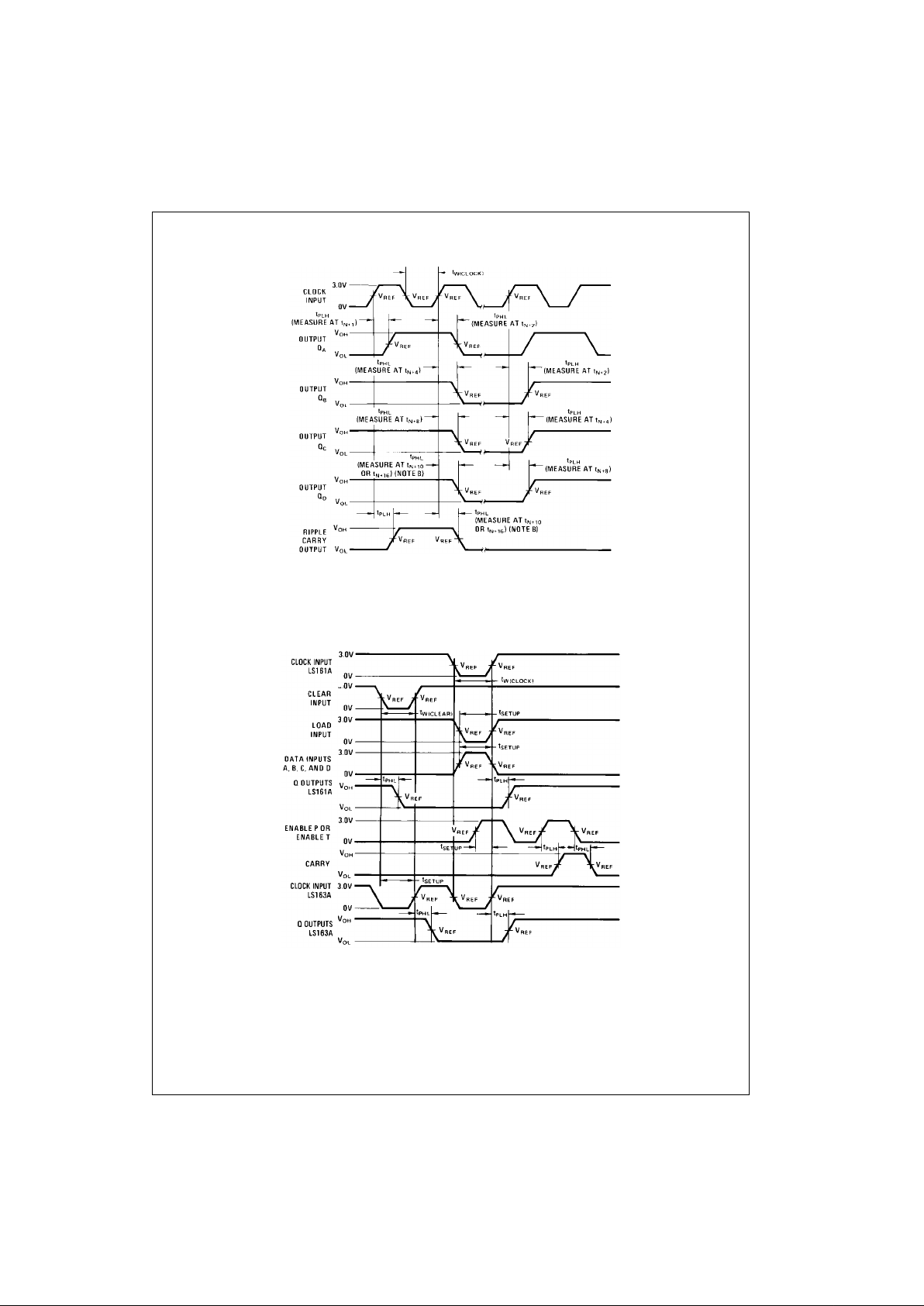
Parameter Measurement Information
Switching Time Wa veforms
The input pulses are supplied by generators having the following characteristics:
PRR ≤ 1 MHz, duty cycle ≤ 50%, Z
OUT
≈ 50Ω, tR ≤ 10 ns, tF ≤ 10 ns.
Vary PRR to measure f
MAX
.
Outputs Q
D
and carry are tested at t
N+16
where tN is the bit time when all o ut puts are LOW.
V
REF
= 1.5V.
Switching Time Wa veforms
The input pulses are supplied by generators having the following characteristics:
PRR ≤ 1 MHz, duty cycle ≤ 50%, Z
OUT
≈ 50Ω, tR ≤ 6 ns, tF ≤ 6 ns. Vary PRR to measure f
MAX
.
Enable P and enable T s et up times are measured at t
N+0
.
V
REF
= 1.3V.
 Loading...