

Fairchild Semiconductor DM74AS805BWM, DM74AS805BN Datasheet
DM74AS805B
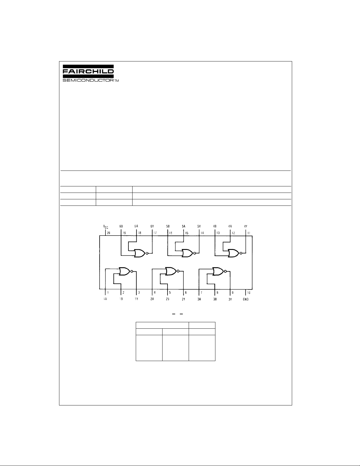
Hex 2-Input NOR Driver
DM74AS805B Hex 2-Input NOR Driver
October 1986
Revised April 2000
General Description
These devices contain six independent drivers, each of
which performs the logic NOR function. Each driver has
increased output drive capability to allow the driving of high
capacitive loads.
Features
■ Switching specifications at 50 pF
■ Switching specifications guaranteed over full tempera-
ture and V
■ Advanced oxide-isolated, ion-implanted Schottky TTL
process
■ Functionally and pin for pin compatible with advanced
low power Schottky TTL counterpart
CC
range
Ordering Code:
Order Number Package Number Package Description
DM74AS805BWM M20B 20-Lead Small Outline Integrated Circuit (SOIC), JEDEC MS-013, 0.300 Wide
DM74AS805BN N20A 20-Lead Plastic Dual-In-Line Package (PDIP), JEDEC MS-001, 0.300 Wide
Devices also availab le in Tape and Reel. Specify by appending the suffix letter “X” to the o rdering code.
Connection Diagram
Function Table
Y = A + B
Inputs Output
ABY
LLH
LHL
HLL
HHL
H = HIGH Logic Le v el
L = LOW Logic Level
© 2000 Fairchild Semiconductor Corporation DS006327 www.fairchildsemi.com
Absolute Maximum Ratings(Note 1)
Supply Voltage 7V
Input Voltage 7V
Operating Free Air Temperature Range 0°C to +70°C
Storage Temperature Range −65°C to +150°C
DM74AS805B
Typical θ
JA
N Package 58.3°C/W
M Package 154.0°C/W
Note 1: The “Absolute Maximum Ratings” are those values beyond which
the safety of the d evice cannot be guaranteed. The device sh ould not be
operated at these limit s. The parametric values defin ed in the Electrical
Characteristics tables are not guaranteed at the absolute maximum ratings.
The “Recomme nded O peratin g Cond itions ” table will defin e the condition s
for actual device operation.
Recommended Operating Conditions
Symbol Parameter Min Nom Max Units
V
CC
V
IH
V
IL
I
OH
I
OL
T
A
Supply Voltage 4.5 5 5.5 V
HIGH Level Input Voltage 2 V
LOW Level Input Voltage 0.8 V
HIGH Level Output Current −48 mA
LOW Level Output Current 48 mA
Free Air Operating Temperature 0 70 °C
Electrical Characteristics
over recommended operating free air temperature range. All typical values are measured at V
Symbol Parameter Conditions Min Typ Max Units
V
IK
V
OH
V
OL
I
I
I
IH
I
IL
I
O
I
CC
Input Clamp Voltage VCC = 4.5V, II = −18 mA −1.2 V
HIGH Level IOH = −2 mA, VCC = 4.5V to 5.5V VCC − 2
Output Voltage IOH = −3 mA, VCC = 4.5V 2.4 V
LOW Level VCC = 4.5V,
Output Voltage IOL = Max
Input Current @ Max Input Voltage VCC = 5.5V, VIH = 7V 0.1 mA
HIGH Level Input Current VCC = 5.5V, VIH = 2.7V 20 µA
LOW Level Input Current VCC = 5.5V, VIL = 0.4V −0.5 mA
Output Drive Current VCC = 5.5V, VO = 2.25V −50 −135 −200 mA
Supply Current VCC = 5.5V Outputs HIGH 6.5 10 mA
I
= Max, VCC = 4.5V 2
OH
Outputs LOW 18 32 mA
CC
= 5V, T
= 25°C.
A
0.35 0.5 V
Switching Characteristics
over recommended operating free air temperature range
Symbol Parameter Conditions Min Max Units
t
PLH
t
PHL
www.fairchildsemi.com 2
Propagation Delay Time VCC = 4.5V to 5.5V
LOW-to-HIGH Level Output RL = 500Ω
Propagation Delay Time CL = 50 pF
HIGH-to-LOW Level Output
14.3 ns
14.3 ns
 Loading...