September 1195
Revised March 1999
CGS3321 • CGS3322 CMOS Crystal Clock Generators
© 1999 Fairchild Semiconductor Corporation DS011503.prf www.fairchildsemi.com
CGS3321 • CGS3322
CMOS Crystal Clock Generators
General Description
The CGS3321 and CGS3322 devices are designed for
Clock Generation and Support (CGS) application s up to
110 MHz. The CGS332x series of devices are crystal controlled CMOS oscillators requiring a minimum of external
components. The 332x dev ices provide selectable output
divide ratio. The c ircuit is designed to operat e over a wide
frequency range using fundamental mode or overtone crystals.
Features
■ Fairchild’s CGS family of devices for high frequency
clock source applications
■ Crystal frequency operation range:
fundamental: 10 MHz to 100 MHz typical
3rd or 5th overtone: 10 MHz to 95 MHz
■ 1000V ESD protection on OC S_IN an d OSC_O UT pins .
2000V ESD protection on all other pins
■ Output current drive of 48 mA for I
OL/IOH
■ FACT CMOS output levels
■ Output has high speed short circuit protection
■ Intended for Pierce oscillator applications
■ Hysteresis inputs to improve noise margin
■ CGS3321 has duty cycle adjust
■ CGS3322 has 1, 2, 4 divide ratio
Ordering Code:
Devices also availab le in Tape and Reel. Specify by appending th e s uffix let t er “X” to the ordering cod e.
Connection Diagrams
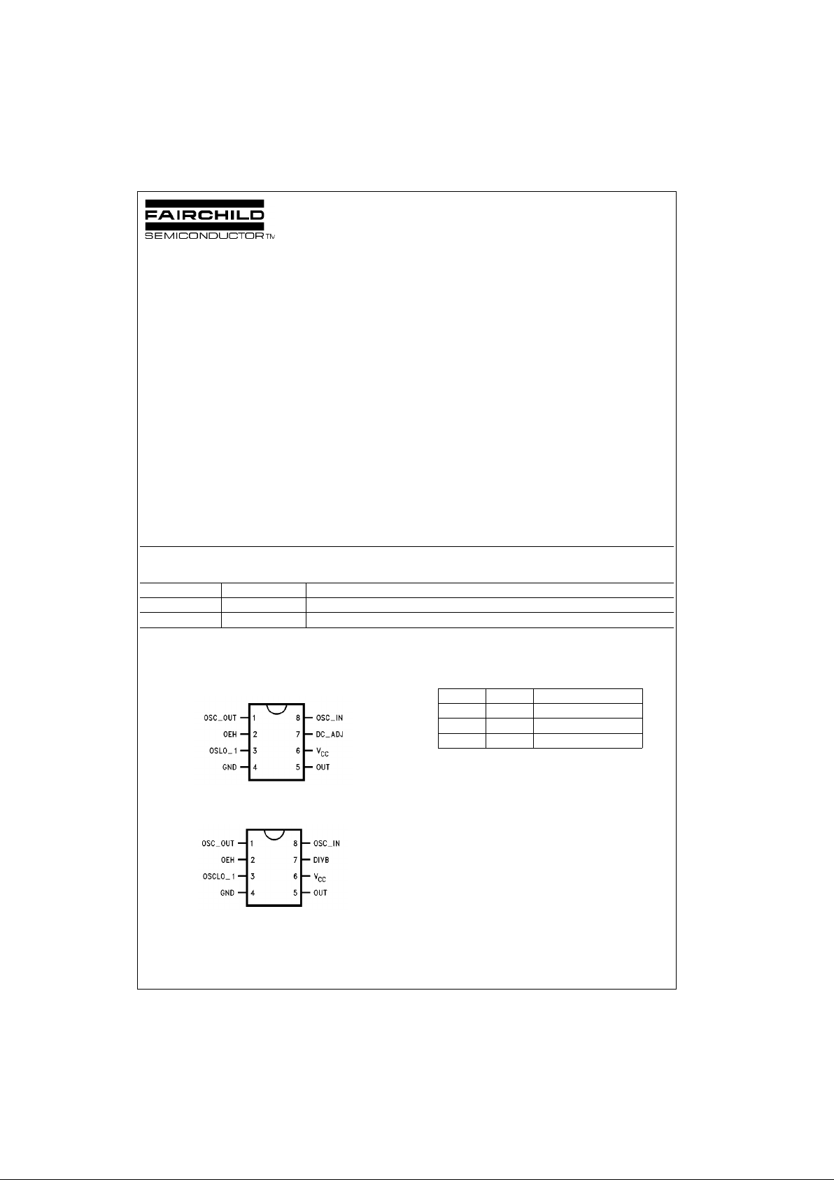
CGS3321
CGS3322
Truth Table
Division Selection
Note: Actual value of the float ing DIVB input is V
CC/2
FACT is a trade m ark of F airchild Semiconductor Corporation.
Order Number Package Number Package Description
CGS3321M M08A 8-Lead Small Outline Integrated Circuit (SOIC), JEDEC MS-012, 0.150” Narrow Body
CGS3322M M08A 8-Lead Small Outline Integrated Circuit (SOIC), JEDEC MS-012, 0.150” Narrow Body
DIVB OEH Divider Output
F X Divide-by 1
1 1 Divide-by 2
0 1 Divide-by 4

www.fairchildsemi.com 2
CGS3321 • CGS3322
Pin Descriptions
Note: Pin out varies for each device.
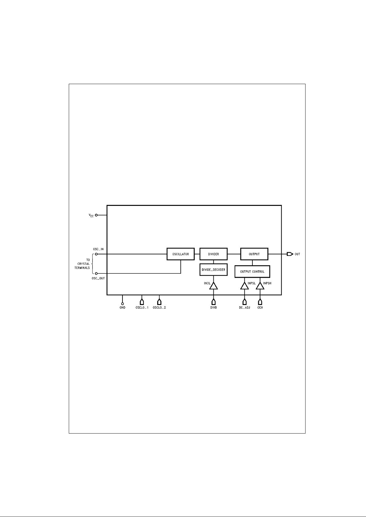
Block Diagrams
Note: Pin numbers vary for each device
Note: Pin out varies for each device.
OSC_IN Input to Oscillator Inverter. The output of the
crystal would be connected here.
OEH Active HIGH 3-STATE enable pin. This pin pulls
to a HIGH value when left floating and 3STATEs the output when forced LOW. This pin
has TTL compatible input levels.
OSC_OUT Resistive Buffered Output of the Oscillator
Inverter
OUT This pin is the main clock output on the device.
DIVB (CGS3322 only)
3-Level input used to select Binary Divide-by
value of output frequency.
OSCLO_1 The Oscillator LOW pin is the ground for the
Oscillator.
DC_ADJ (CGS3321 only)
Active high input that controls output duty
cycle. Logic high level will delay the HL transition edge approximately 0.3 ns.
V
CC
The power pin for the chip.
GND The ground pin for all sections of the circuitry
except the oscillator and oscillator related
circuitry.
 Loading...