Fairchild Semiconductor CGS3318MX, CGS3318M Datasheet

September 1995
Revised March 1999
CGS3311 • CGS3312 • CGS3313 • CGS3314 • CGS3315 • CGS3316 • CGS3317 • CGS3318 • CGS3319 CMOS Crystal
Clock Generators
© 1999 Fairchild Semiconductor Corporation DS010980.prf www.fairchildsemi.com
CGS3311 • CGS3312 • CGS3313 • CGS3314 • CGS3315 •
CGS3316 • CGS3317 • CGS3318 • CGS3319
CMOS Crystal Clock Generators
General Description
The CGS3311, CGS3312, CGS3313, CGS3314,
CGS3315, CGS3316 , CGS 3317, CGS33 18 an d CGS33 19
devices are designed for Clock Generation and Support
(CGS) applications up to 110 MHz. The CGS331x series of
devices are crystal controlled CMOS oscillators requiring a
minimum of external components. The 331x devices provide selectable output divide ratio (a nd selectable crystal
drive level). The ci rcuit is designed to operat e over a wide
frequency range using fundamental model or overtone
crystals.
Features
■ Fairchild’s CGS family of devices for high frequency
clock source applications
■ Crystal frequency operation range:
fundamental: 10 MHz to 100 MHz typical
3rd or 5th overtone: 10 MHz to 85 MHz
■ Programmable oscillator drive
■ Selectable fast output edge rates
■ Output symmetry circuit to adjust 50% duty cycle point
between CMOS and TTL levels
■ Output current drive of 48 mA for I
OL/IOH
■ FACT CMOS output levels
■ Output has high speed short circuit protection
■ Basic oscillator type: Pierce
■ Hysteresis inputs to improve noise margin
Ordering Code:
Devices also availab le in Tape and Reel. Specify by appending th e s uffix let t er “X” to the ordering cod e.
FACT is a trade m ark of F airchild Semicondu ctor Corporation.
Order Number Package Number Package Description
CGS3311M M08A 8-Lead Small Outline Integrated Circuit (SOIC), JEDEC MS-012, 0.150” Narrow Body
CGS3312M M08A 8-Lead Small Outline Integrated Circuit (SOIC), JEDEC MS-012, 0.150” Narrow Body
CGS3313M M08A 8-Lead Small Outline Integrated Circuit (SOIC), JEDEC MS-012, 0.150” Narrow Body
CGS3314M M08A 8-Lead Small Outline Integrated Circuit (SOIC), JEDEC MS-012, 0.150” Narrow Body
CGS3315M M08A 8-Lead Small Outline Integrated Circuit (SOIC), JEDEC MS-012, 0.150” Narrow Body
CGS3316M M08A 8-Lead Small Outline Integrated Circuit (SOIC), JEDEC MS-012, 0.150” Narrow Body
CGS3317M M08A 8-Lead Small Outline Integrated Circuit (SOIC), JEDEC MS-012, 0.150” Narrow Body
CGS3318M M08A 8-Lead Small Outline Integrated Circuit (SOIC), JEDEC MS-012, 0.150” Narrow Body
CGS3319M M08A 8-Lead Small Outline Integrated Circuit (SOIC), JEDEC MS-012, 0.150” Narrow Body

www.fairchildsemi.com 2
CGS3311 • CGS3312 • CGS3313 • CGS3314 • CGS3315 • CGS3316 • CGS3317 • CGS3318 • CGS3319
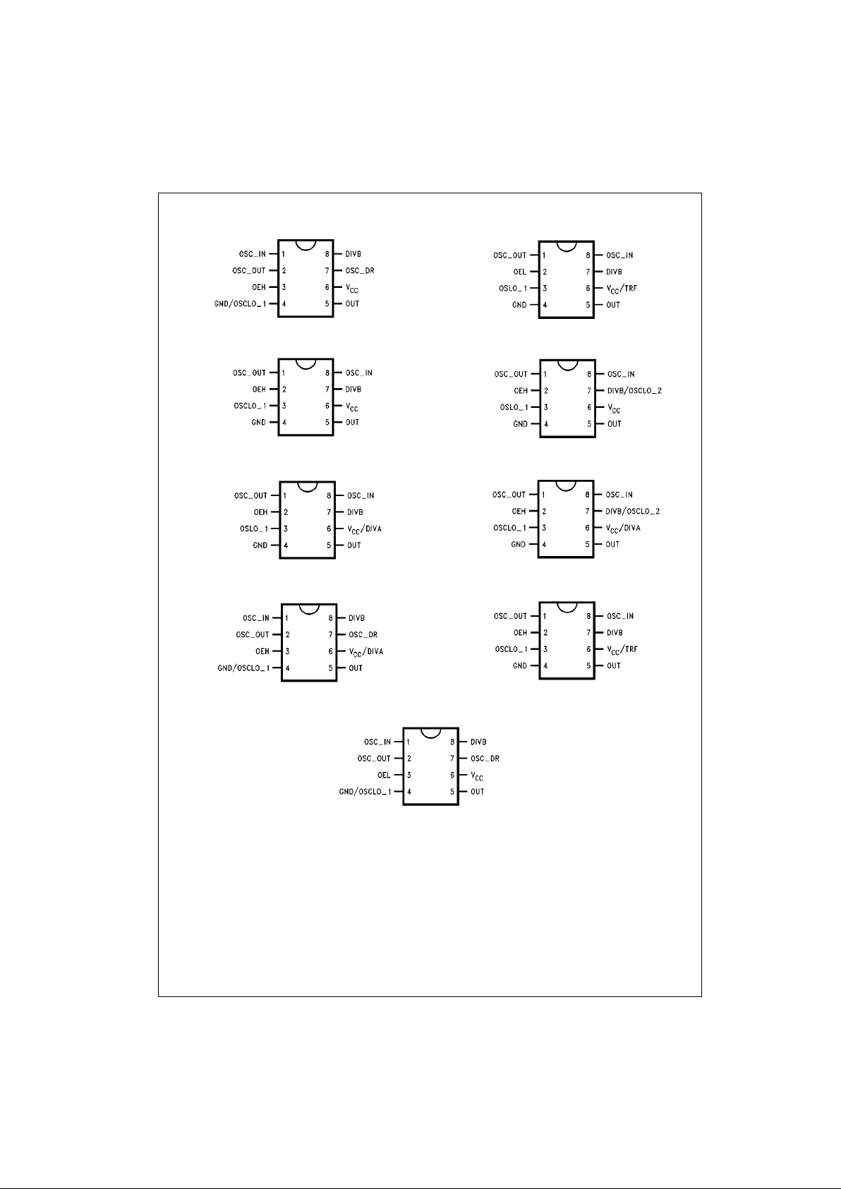
Connection Diagrams
(A) 3311
(B)3312
(C) 3313
(D) 3314
(E) 3315
(F) 3316
(G) 3317
(H) 3318
(I) 3319

3 www.fairchildsemi.com
CGS3311 • CGS3312 • CGS3313 • CGS3314 • CGS3315 • CGS3316 • CGS3317 • CGS3318 • CGS3319
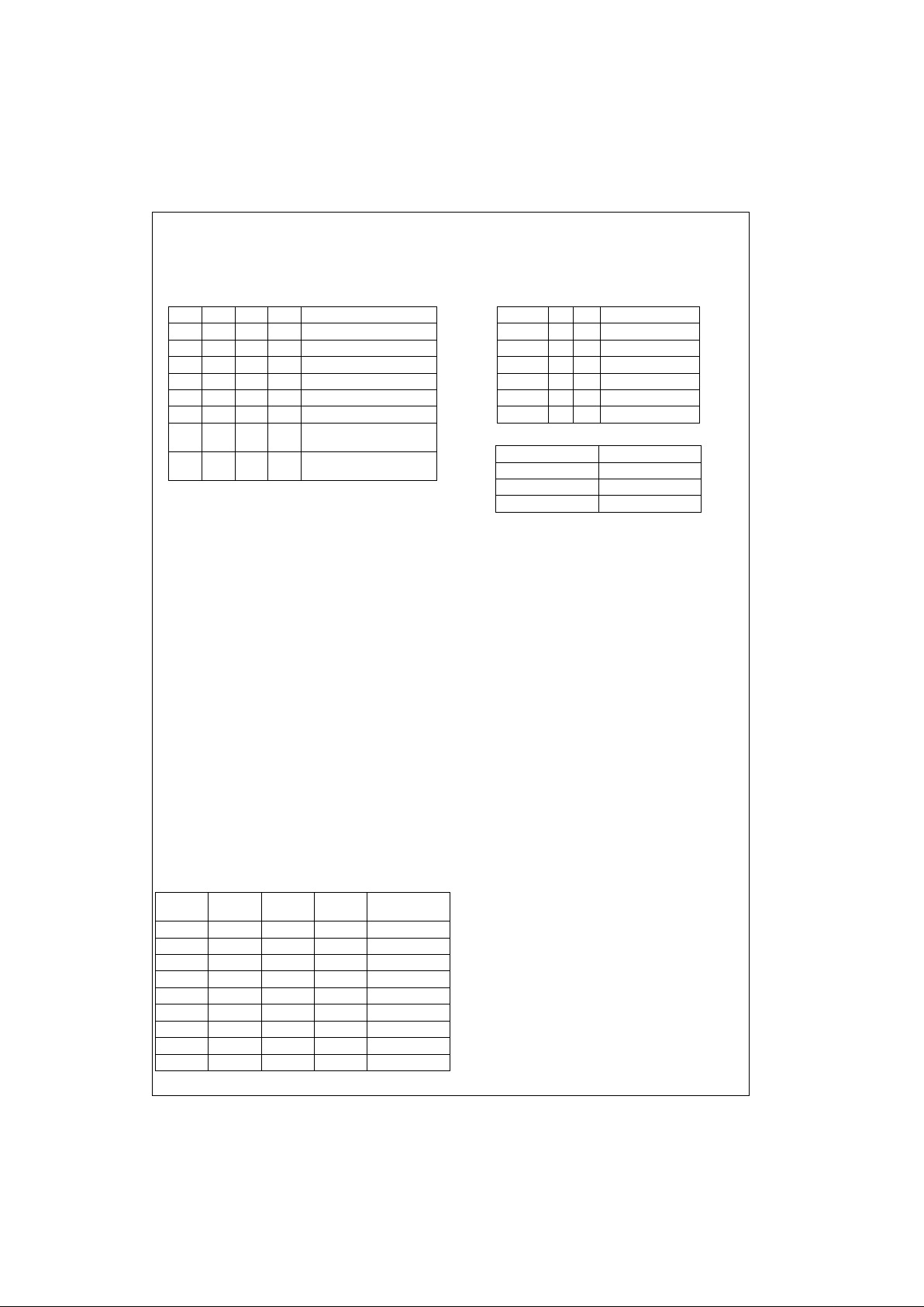
Truth Tables
Division Selection
Note: Actual value of the fl oat ing OSC_DR and DIV B input is V
CC/2
Rise and Fall Time Selection
Drive Selection
Note: Where “F” indicates floating the input.
Pin Descriptions
Functional Table
Summary of Device Options
Each drive has one output with the choices of selecting frequency divide,
output enable, c rystal drive and output rise and fall time. Crystal drive
options are:
L = LOW Drive
M = MEDIUM Drive
H = HIGH Drive
DIVB DIVA OEL OEH Divider Output
F 0/F X X Divide-by 1
1 0/F 0 1 Divide-by 2
0 0/F 0 1 Divide-by 4
F 1 0 1 Divide-by 8
1 1 0 1 Divide-by 16
0 1 0 1 Divide-by 32
X X 1 X Output Reset HIGH
at Re-enable
X X X 0 Output Reset HIGH
at Re-enable
OSC_DR DIV TRF Rise/Fall Time (ns)
FN0/F2
F N 1 less than 2
FY0/F4
FY12
0,1 X 0/F 4
0,1 X 1 2
OSC_DR Drive
0Low
1 Medium
F High
Note: Pin out varies for each device.
OSC_IN Input to Oscillator Inverter. The output of the
crystal would be connected here.
OEL Active LOW 3-STATE enable pin. This pin pulls
to a low value when left floating and 3-STATE
the output when forced HIGH. This pin has TTL
compatible input levels.
OSC_OUT Resistive Buffered Output of the Oscillator
Inverter
TRF Rise and Fall time override pin. Available only
for die form.
OSC_DR 3 Level input pin that selects Oscillator Drive
Level
OUT This pin is the main clock output on the device.
DIVA Input used to select Binary Divide-by Option.
This pin has CMOS compatible input levels.
OSCLO_1 The Oscillator LOW pin is the ground for the
Oscillator.
OEH Active HIGH 3-STATE enable pin. This pin pulls
to a high value when left floating and 3-STATEs
the output when forced low. This pin has TTL
compatible input levels.
OSCLO_2 This pin is the same signal as OSCLO_1. It has
been provided as an alternate connection for
OSCLO_1 for hybrid assemblies.
V
CC
The power pin for the chip.
GND The ground pin for all sections of the circuitry
except the oscillator and oscillator related
circuitry.
Device Divide Enable Drive
Output Rise/
Fall Time (ns)
3311 1, 2, 4 OEH L, M, H 2, 4
3312 1, 2, 4 OEH H 2, 4
3313 8, 16, 32 O E H H 4
3314 8, 16, 32 O E H L, M, H 4
3315 1, 2, 4 OEL H 1, 2
3316 4 OEH H 4
3317 32 OEH H 4
3318 1, 2, 4 OEH H 1, 2
3319 1, 2, 4 OEL L, M, H 2, 4
 Loading...