

Fairchild Semiconductor 74ACT843SPC, 74ACT843SCX, 74ACT843SC, 74ACT843CW Datasheet
© 2000 Fairchild Semiconductor Corporation DS009800 www.fairchildsemi.com
July 1988
Revised September 2000
74ACT843 9-Bit Transparent Latch
74ACT843
9-Bit Transparent Latch
General Description
The ACT843 bus inter face latch is designed to e liminate
the extra packages required to buffer existing latch es and
provide extra data width for wider address/data paths.
Features
■ TTL compatible inputs
■ 3-STATE outputs for bus interfacing
Ordering Code:
Device also available in Tape and Reel. Specify by appending s uffix let te r “X” to the ordering code. (SPC not available in Tape and Reel.)
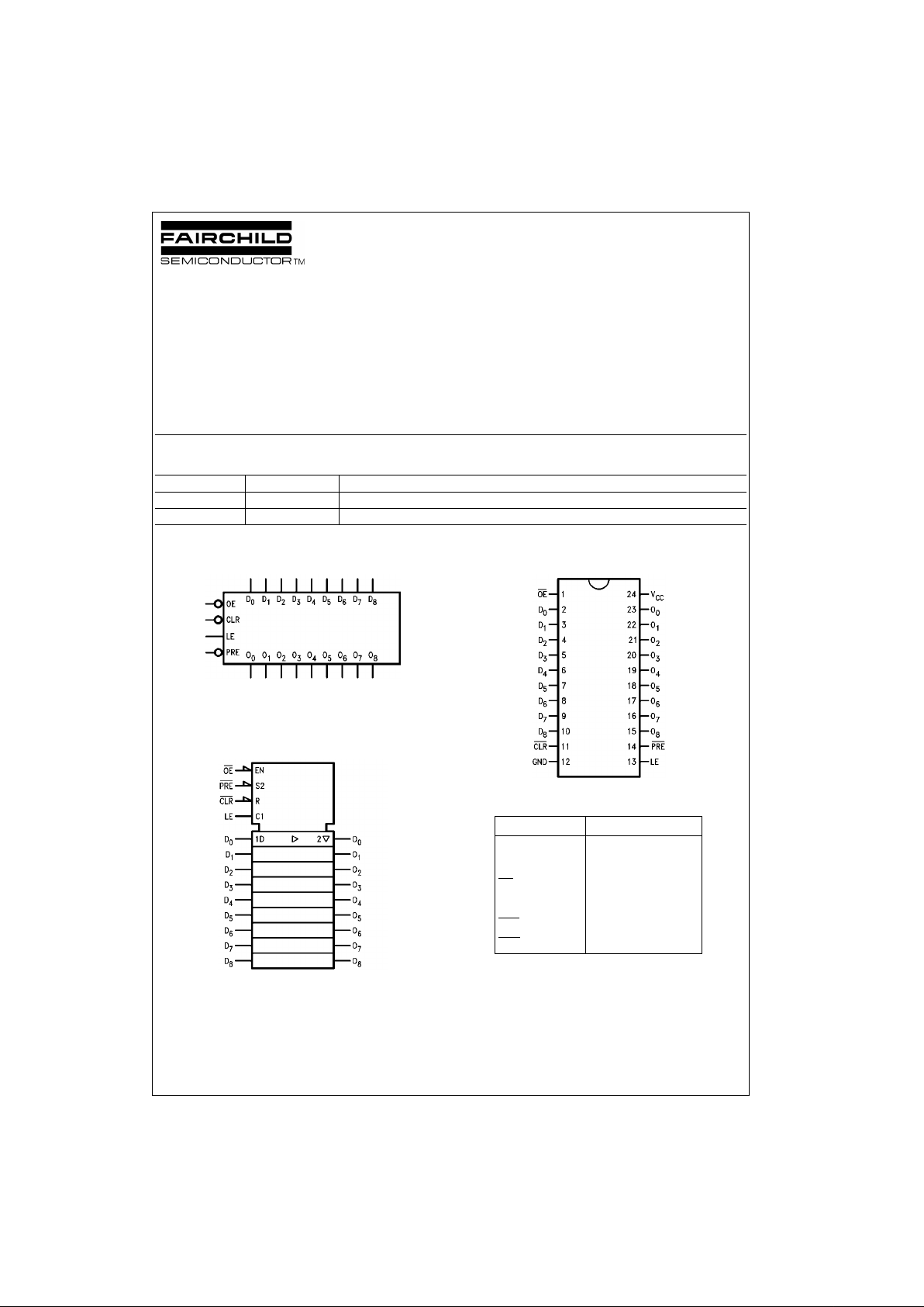
Logic Symbols
IEEE/IEC
Connection Diagram
Pin Descriptions
FACT is a trademark of Fairchild Semiconductor Corporation
Order Number Package Number Package Description
74ACT843SC M24B 24-Lead Small Outline Integrated Circuit (SOIC), JEDEC MS-013, 0.300 Wide
74ACT843SPC N24C 24-Lead Plastic Dual-In-Line Package (PDIP), JEDEC MS-001, 0.300 Wide
Pin Names Description
D
0–D8
Data Inputs
O
0–O8
Data Outputs
OE
Output Enable
LE Latch Enable
CLR
Clear
PRE
Preset
www.fairchildsemi.com 2
74ACT843
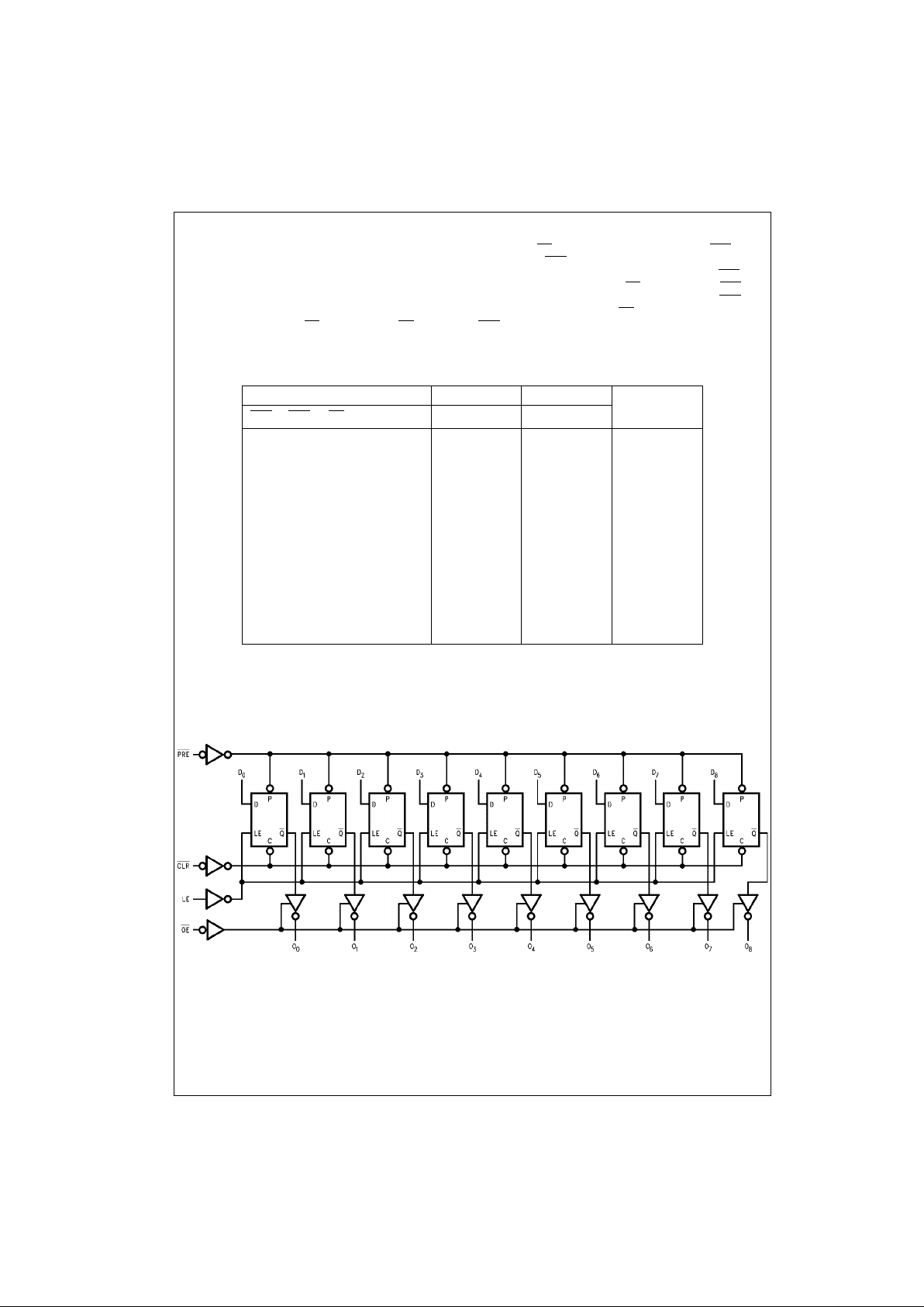
Functional Description
The ACT843 consists of nine D-t ype latches with 3 -STATE
outputs. The flip-flops a ppe ar tran spa ren t to th e da ta w he n
Latch Enable (LE) is HIGH. This allows asynchronous
operation, as the output transition follows the data in transition. On the LE HIGH-to-LOW transition, the data that
meets the setup times is latched. Data appears on the bus
when the Output Enabl e (OE
) is LOW. When OE is HIGH,
the bus output is in the high impedance state. In addition to
the LE and OE
pins, the ACT843 has a Clear (CLR) pin
and a Preset (PRE
) pin. These pins are idea l f or p ari t y bus
interfacing in high performance systems. When CLR
is
LOW, the outputs are LOW if OE
is LOW. When CLR is
HIGH, data can be entere d into the latch. When PRE
is
LOW, the outputs are HIGH if OE
is LOW. Preset overrides
CLR
.
Function Tables
H = HIGH Voltage Level
L = LOW Voltage Level
X = Immaterial
Z = High Impedance
NC = No Change
Logic Diagram
Inputs Internal Outputs
Function
CLR
PRE OE LE D Q O
HHHHL L Z High Z
HHHHH H Z High Z
H H H L X NC Z Latched
H H L H L L L Transparent
H H L H H H H Transparent
H H L L X NC NC Latched
H L L X X H H Preset
L H L X X L L Clear
LLLXX H H Preset
L H H L X L Z Clear/High Z
H L H L X H Z Preset/High Z
 Loading...