

Fairchild Semiconductor 74ACT841SCX, 74ACT841SC, 74ACT841MTCX, 74ACT841MTC, 74ACT841CW Datasheet
© 2000 Fairchild Semiconductor Corporation DS010156 www.fairchildsemi.com
November 1988
Revised September 2000
74ACT841 10-Bit Transparent Latch with 3-STATE Outputs
74ACT841
10-Bit Transparent Latch with 3-STATE Outputs
General Description
The ACT841 bus inter face latch is designed to e liminate
the extra packages required to buffer existing latch es and
provide extra data width for wider address/data paths or
buses carrying parity. The ACT841 is a 10-bit transpare nt
latch, a 10-bit version of the ACT373.
Features
■ ACT841 has TTL-compatible inputs
■ Outputs source/sink 24 mA
■ Non-inverting 3-STATE outputs
Ordering Code:
Device also available in Tape and Reel. Specify by appending s uffix let te r “X” to the ordering code. (SPC not available in Tape and Reel.)
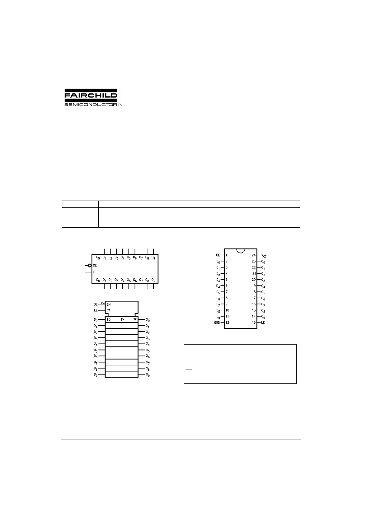
Logic Symbols
IEEE/IEC
Connection Diagram
Pin Descriptions
FACT is a trademark of Fairchild Semiconductor Corporation.
Order Number Package Number Package Description
74ACT841SC M24B 24-Lead Small Outline Integrated Circuit (SOIC), JEDEC MS-013, 0.300 Wide
74ACT841MTC MTC24 24-Lead Thin Shrink Small Outline Package (TSSOP), JEDEC MO-153, 4.4mm Wide
74ACT841SPC N24C 24-Lead Plastic Dual-In-Line Package (PDIP), JEDEC MS-001, 0.300 Wide
Pin Names Description
D
0–D9
Data Inputs
O
0–O9
3-STATE Outputs
OE
Output Enable
LE Latch Enable
www.fairchildsemi.com 2
74ACT841
Functional Description
The ACT841 consists of ten D-type latches with 3-STATE
outputs. The flip-flops a ppe ar tran spa ren t to th e da ta w he n
Latch Enable (LE) is HIGH. This allows asynchronous
operation, as the output transition follows the data in transition.
On the LE HIGH-to-LOW transition, the data that meets the
setup and hold time is latch ed. Data appears on the bus
when the Output Enable (OE
) is LOW. When OE is HIGH
the bus output is in the high impedance state.
Function Table
H = HIGH Voltage Level
L = LOW Voltage Level
X = Immaterial
Z = High Impedance
NC = No Change
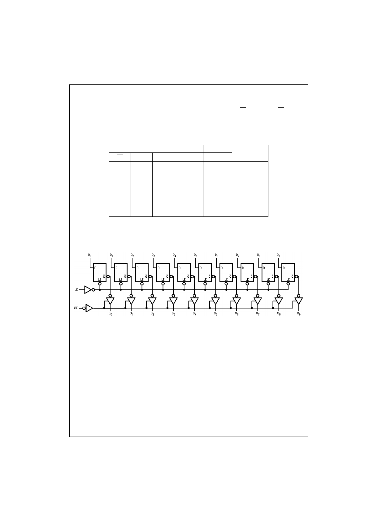
Logic Diagram
Please note that this diagram is provided only for the understanding of logic operations and should not be used to estimate propagation delays.
Inputs Internal Output
Function
OE
LE D Q O
X X X X Z High Z
H H L L Z High Z
H H H H Z High Z
H L X NC Z Latched
L H L L L Transparent
L H H H H Transparent
L L X NC NC Latched
3 www.fairchildsemi.com
74ACT841
Absolute Maximum Ratings(Note 1) Recommended Operating
Conditions
Note 1: Absolute max imum ratings are those values beyond w hich damage
to the device may occu r. The databook spe cificatio ns shou ld be met, wit hout exception, to ensure that the system de sign is relia ble over its p ower
supply, temperature, and output/input loading variables. Fairchild does not
recommend operation of FACT circuits outside databook specif ic at ions.
DC Electrical Characteristics
Note 2: All outputs loaded; thres holds on input associate d w it h output under test.
Note 3: Maximum test duration 2.0 ms, one output loaded at a time.
Supply Voltage (VCC) −0.5V to +7.0V
DC Input Diode Current (I
IK
)
V
I
= −0.5V −20 mA
V
I
= VCC + 0.5V +20 mA
DC Input Voltage (V
I
) −0.5V to VCC + 0.5V
DC Output Diode Current (I
OK
)
V
O
= −0.5V −20 mA
V
O
= VCC + 0.5V +20 mA
DC Output Voltage (V
O
) −0.5V to VCC + 0.5V
DC Output Source
or Sink Current (I
O
) ±50 mA
DC V
CC
or Ground Current
per Output Pin (I
CC
or I
GND
) ±50 mA
Storage Temperature (T
STG
) −65°C to +150°C
Junction Temperature (T
J
)
PDIP 140
°C
Supply Voltage (V
CC
) 4.5V to 5.5V
Input Voltage (V
I
) 0V to V
CC
Output Voltage (VO) 0V to V
CC
Operating Temperature (TA) −40°C to +85°C
Minimum Input Edge Rate (
∆V/∆t) 125 mV/ns
V
IN
from 0.8V to 2.0V
V
CC
@ 4.5V, 5.5V
Symbol Parameter
V
CC
TA = +25°CT
A
= −40°C to +85°C
Units Conditions
(V) Typ Guaranteed Limits
V
IH
Minimum HIGH Level 4.5 1.5 2.0 2.0
V
V
OUT
= 0.1V
Input Voltage 5.5 1.5 2.0 2.0 or VCC − 0.1V
V
IL
Maximum LOW Level 4.5 1.5 0.8 0.8
V
V
OUT
= 0.1V
Input Voltage 5.5 1.5 0.8 0.8 or VCC − 0.1V
V
OH
Minimum HIGH Level 4.5 4.49 4.4 4.4
V I
OUT
= −50 µA
Output Voltage 5.5 5.49 5.4 5.4
VIN = VIL or V
IH
4.5 3.86 3.76 V IOH = −24 mA
5.5 4.86 4.76 IOH = −24 mA (Note 2)
V
OL
Maximum LOW Level 4.5 0.001 0.1 0.1
V I
OUT
= 50 µA
Output Voltage 5.5 0.001 0.1 0.1
VIN = VIL or V
IH
4.5 0.36 0.44 V IOL = 24 mA
5.5 0.36 0.44 I
OL
= 24 mA (Note 2)
I
IN
Maximum Input
5.5 ±0.1 ±1.0 µA V
I
= VCC, GND
Leakage Current
I
OZ
Maximum 3- STATE
5.5 ±0.5 ±5.0 µA
VI = VIL, V
IH
Leakage Current VO = VCC, GND
I
CCT
Maximum
5.5 0.6 1.5 µA VI = VCC − 2.1V
ICC/Input
I
OLD
Minimum Dynamic 5.5 75 mA V
OLD
= 1.65V Max
I
OHD
Output Current (Note 3) 5.5 −75 mA V
OHD
= 3.85V Min
I
CC
Maximum Quiescent
5.5 8.0 80.0 µA
VIN = V
CC
Supply Current or GND
 Loading...