

Fairchild Semiconductor 74ACT825SCX, 74ACT825SC, 74ACT825MTCX, 74ACT825MTC, 74ACT825CW Datasheet
© 2000 Fairchild Semiconductor Corporation DS009895 www.fairchildsemi.com
July 1988
Revised September 2000
74ACT825 8-Bit D-Type Flip-Flop
74ACT825
8-Bit D-Type Flip-Flop
General Description
The ACT825 is an 8-bit b uffered re giste r. They have Clock
Enable and Clear features which are ideal for parity bus
interfacing in high performance microprogramming systems. Also included are multiple enables that allow multiuse control of the interface. The ACT825 has noninverting
outputs.
Features
■ Outputs source/sink 24 mA
■ Inputs and outputs are on opposite sides
■ TTL compatible inputs
Ordering Code:
Device also available in Tape and Reel. Specify by appending s uffix let te r “X” to the ordering code.
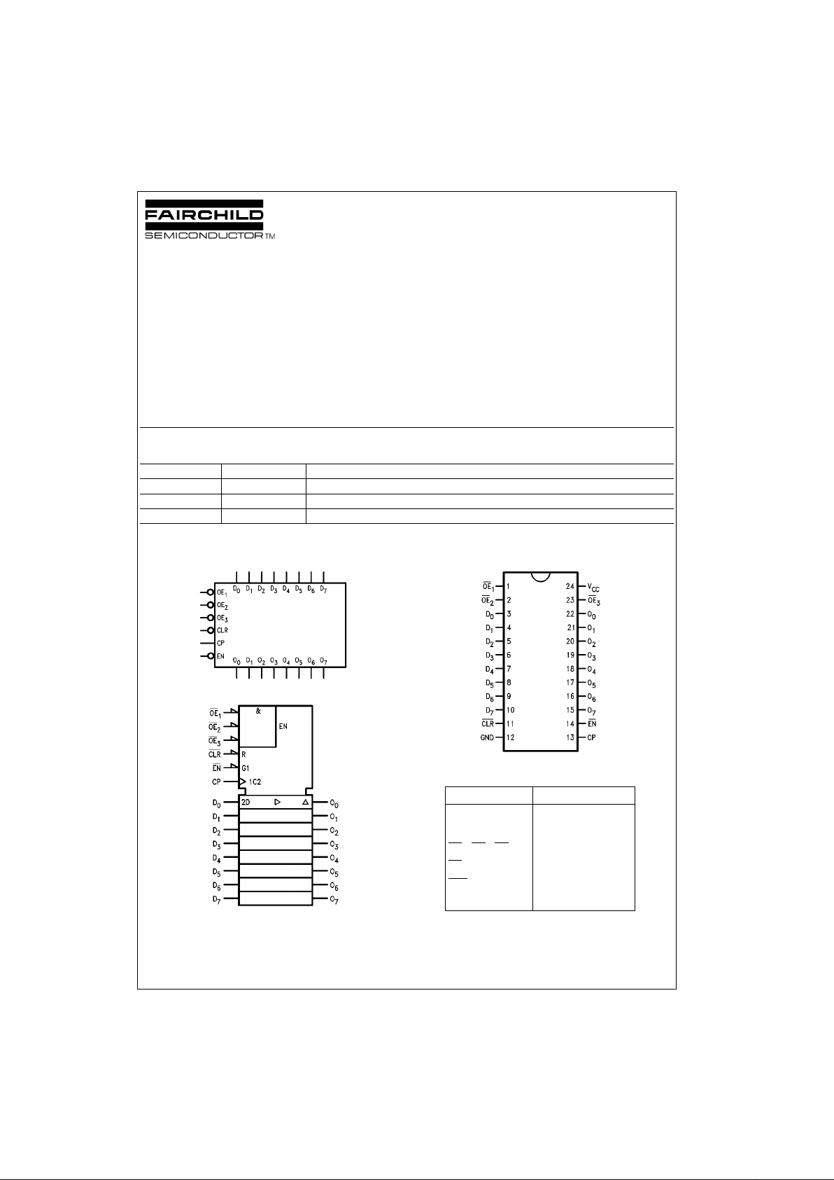
Logic Symbols
IEEE/IEC
Connection Diagram
Pin Descriptions
FACT is a trademark of Fairchild Semiconductor.
Order Number Package Number Package Description
74ACT825SC M24B 24-Lead Small Outline Integrated Circuit (SOIC), JEDEC MS-013, 0.300 Wide
74ACT825MTC MTC24 24-Lead Thin Shrink Small Outline Package (TSSOP), JEDEC MO-153, 4.4mm Wide
74ACT825SPC N24C 24-Lead Plastic Dual-In-Line Package (PDIP), JEDEC MS-001, 0.300 Wide
Pin Names Description
D
0–D7
Data Inputs
O
0–O7
Data Outputs
OE
1
, OE2, OE3Output Enables
EN
Clock Enable
CLR
Clear
CP Clock Input
www.fairchildsemi.com 2
74ACT825
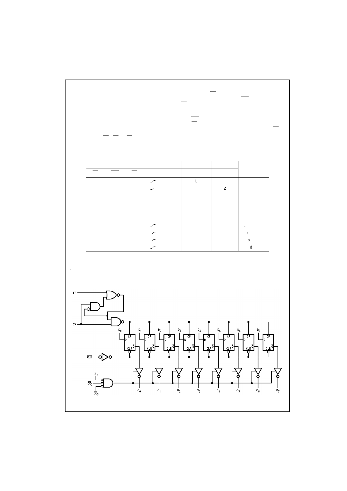
Functional Description
The ACT825 consists of eight D-type edge-triggered flipflops. These devices have 3-STATE outputs for bus systems, organized in a broadside pinning. In addition to the
clock and output enable pins , the buffered clock (CP) and
buffered Output En able (OE
) are common to all flip-flops.
The flip-flops will store the state of their individual D inputs
that meet the setup and hold time requirements on the
LOW-to-HIGH CP transition. With OE
1
, OE2 and OE
3
LOW, the contents of the flip-flops a re availa ble a t the ou tputs. When one of OE
1
, OE2 or OE3 is HIGH, the outputs
go to the high impedance state.
Operation of the O E
input does not affect the state of the
flip-flops. The ACT825 has Clear (CLR
) and Clock Enable
(EN
) pins. These pins a re ideal for p arity bus inter fac ing in
high performance systems.
When CLR
is LOW and OE is LOW, the outputs are LO W.
When CLR
is HIGH, data can be entered into the flip-f lops.
When EN
is LOW, data on the inputs is transferred to the
outputs on the LOW-to-HIGH clock transition. When EN
is
HIGH, the outputs do not change state , regardless of the
data or clock input transitions.
Function Table
H = HIGH Voltage Level
L = LOW Voltage Level
X = Immaterial
Z = High Impedance
= LOW-to-HIGH Transition
NC = No Change
Logic Diagram
Please note that this diagram is provided only for the understanding of logic operations and should not be used to estimate propagation d elays.
Inputs Internal Output
Function
OE
CLR EN CP D
n
QO
HXL
L L Z High-Z
HXL
H H Z High-Z
H L XXX L Z Clear
L L XXX L L Clear
H H H X X NC Z Hold
LHHXX NC NCHold
HHL
L L Z Load
HHL
H H Z Load
LHL
L L L Load
LHL
H H H Load
3 www.fairchildsemi.com
74ACT825
Absolute Maximum Ratings(Note 1) Recommended Operating
Conditions
Note 1: Absolute max imum ratings are those values beyond which damage
to the device may occu r. The databook spe cificatio ns shou ld be met, wit hout exception, to ensure that the system de sign is relia ble over its p ower
supply, temperature, and output/input loading variables. Fairchild does not
recommend operation of FACT circuits outside databook specifications.
DC Electrical Characteristics
Note 2: All outputs loaded; thres holds on input associate d w it h output under test.
Note 3: Maximum test duration 2.0 ms, one output loaded at a time.
Supply Voltage (VCC) −0.5V to 7.0V
DC Input Diode Current (I
IK
)
V
I
= −0.5V −20 mA
V
I
= VCC +0.5V +20 mA
DC Input Voltage (V
I
) −0.5V to VCC +0.5V
DC Output Diode Current (I
OK
)
V
O
= −0.5V −20 mA
V
O
= VCC +0.5V +20 mA
DC Output Voltage (V
O
) +0.5V
DC Output Source or Sink Current
(I
O
) ± 50 mA
DC V
CC
or Ground Current
Per Output Pin (I
CC
or I
GND
) ± 50 mA
Storage Temperature (T
STG
) −65°C to +150°C
Junction Temperature (T
J
)
PDIP 140
°C
Supply Voltage (V
CC
) 4.5V to 5.5V
Input Voltage (V
I
)0V to V
CC
Output Voltage (VO)0V to V
CC
Operating Temperature (TA) −40°C to +85°C
Minimum Input Edge Rate (
∆V/∆t) 125 mV/ns
V
IN
from 0.8V to 2.0V
V
CC
@ 4.5V, 5.5V
Symbol Parameter
V
CC
TA = 25°CT
A
= −40°C to +85°C
Units Conditions
(V) Typ Guaranteed Limits
V
IH
Minimum HIGH Level 4.5 1.5 2.0 2.0
V
V
OUT
= 0.1V
Input Voltage 5.5 1.5 2.0 2.0 or VCC −0.1V
V
IL
Maximum LOW Level 4.5 1.5 0.8 0.8
V
V
OUT
= 0.1V
Input Voltage 5.5 1.5 0.8 0.8 or VCC −0.1V
V
OH
Minimum HIGH Level 4.5 4.49 4.4 4.4
VI
OUT
= −50 µA
Output Voltage 5.5 5.49 5.4 5.4
VIN = VIL or V
IH
4.5 3.86 3.76 V IOH = −24 mA
5.5 4.86 4.76 IOH = −24 mA (Note 2)
V
OL
Maximum LOW Level 4.5 0.001 0.1 0.1
VI
OUT
= 50 µA
Output Voltage 5.5 0.001 0.1 0.1
VIN = VIL or V
IH
4.5 0.36 0.44 V IOL = 24 mA
5.5 0.36 0.44 I
OL
= 24 mA (Note 2)
I
IN
Maximum Input Leakage Current 5.5 ± 0.1 ± 1.0 µAVI = VCC, GND
I
OZ
Maximum
5.5 ±0.5 ±5.0 µA
VI = VIL, V
IH
3-STATE Current VO = VCC, GND
I
CCT
Maximum ICC/Input 5.5 0.6 1.5 mA VI = VCC −2.1V
I
OLD
Minimum Dynamic 5.5 75 mA V
OLD
= 1.65V Max
I
OHD
Output Current (Note 3) 5.5 −75 mA V
OHD
= 3.85V Min
I
CC
Maximum Quiescent
5.5 8.0 80 µAVIN = VCC or GND
Supply Current
 Loading...