Fairchild Semiconductor 74ACT16646SSCX, 74ACT16646SSC, 74ACT16646MTDX, 74ACT16646MTD Datasheet

© 1999 Fairchild Semiconductor Corporation DS500345 www.fairchildsemi.com
August 1999
Revised October 1999
74ACT16646 16-Bit Transceiver/Register with 3-STATE Outputs
74ACT16646
16-Bit Transceiver/Register with 3-STATE Outputs
General Description
The ACT16646 contain s sixte en non- inverti ng bidir ectio nal
registered bus transceivers providing multiplexed transmission of data directly from the input bus or from the internal
storage registers. Each byte h as separate control inputs
which can be shorted tog eth er for ful l 1 6-b i t op era ti on . T he
DIR inputs determin e the dir ection of data flow t hro ug h t he
device. The CPAB and CPBA inputs load data into the registers on the LOW-to-HIGH transition.
Features
■ Independent registers for A and B buses
■ Multiplexed real-time and stored data transfers
■ Separate control logic for each byte
■ 16-bit version of the ACT646
■ Outputs source/sink 24 mA
■ TTL-compatible inputs
Ordering Code:
Device also available in Tape and Reel. Specify by appending s uffix let te r “X” to the ordering code.
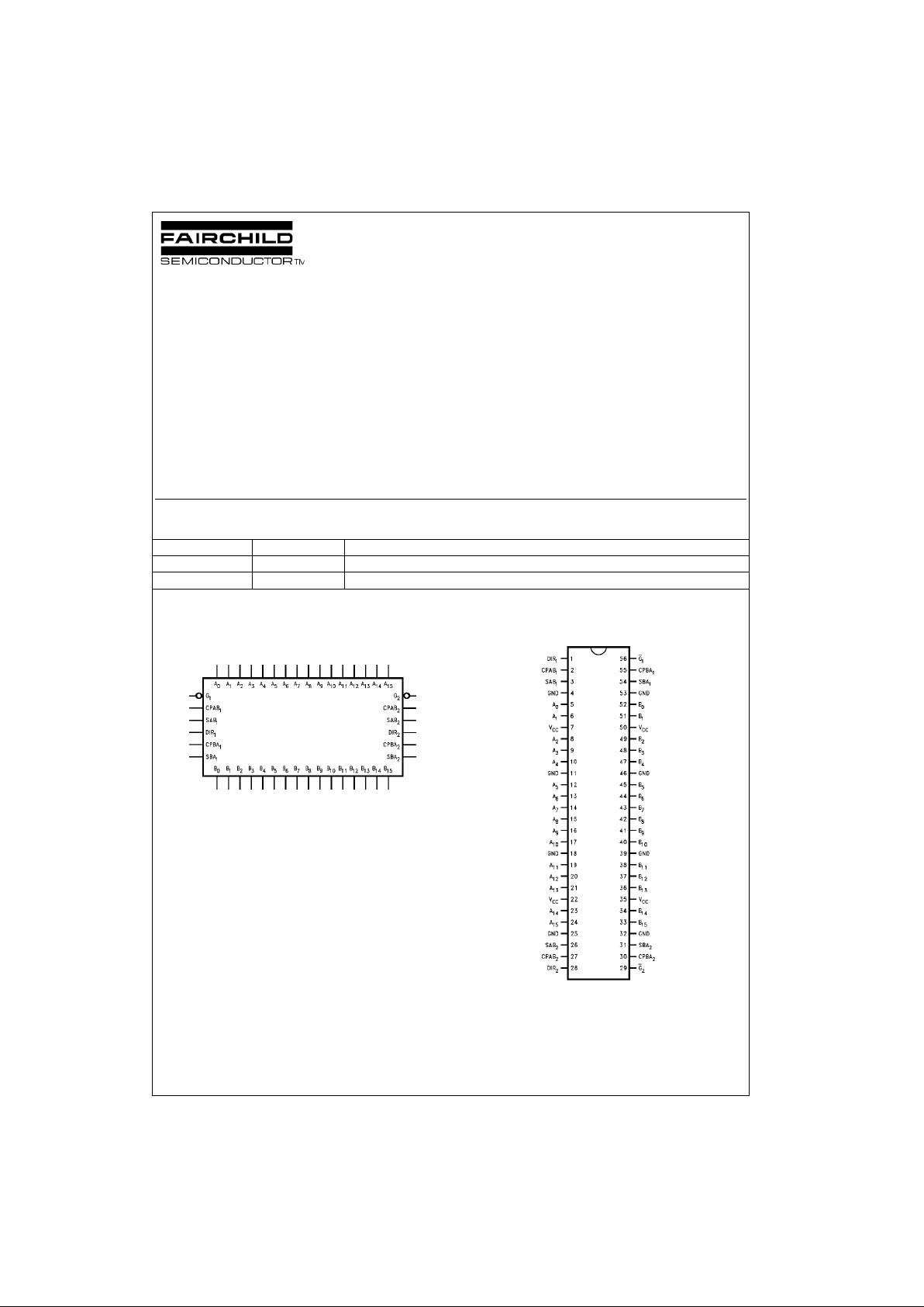
Logic Symbol Connection Diagram
FACT is a trade m ark of F airchild Semicondu ctor Corporation.
Order Number Package Number Package Description
74ACT16646SSC MS56A 56-Lead Shrink Small Outline Package (SSOP), JEDEC MO-118, 0.300” Wide
74ACT16646MTD MTD56 56-Lead Thin Shrink Small Outline Package (TSSOP), JEDEC MO-153, 6.1mm Wide

www.fairchildsemi.com 2
74ACT16646
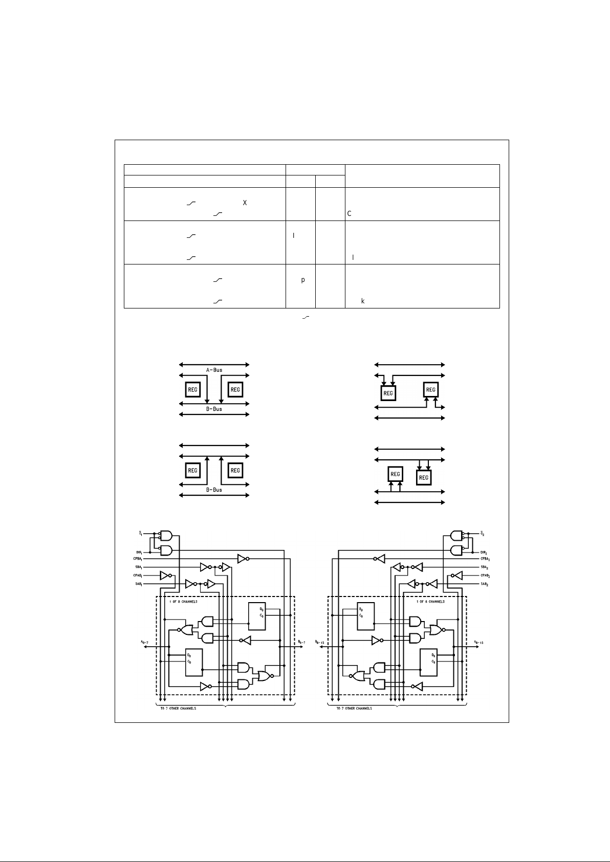
Function Table
H = HIGH Voltage Level X = Immaterial L = LOW Voltage Level = LOW-to-HIGH Transitio n.
Note 1: The data output functions may be enabled or disabled by various signals at the G and DIR inputs. Da ta input fu nct i ons are al way s enabled; i.e., data
at the bus pins will be s to red on every LOW-to-HIGH transition of the appropriate clock inputs. Also applies to data I/O (A and B: 8-15) and #2 control pi ns .
Real Time Transfer
A-Bus to B-Bus
Real Time Transfer
B-Bus to A-Bus
Storage from
Bus to Register
Transfer from
Register to Bus
Logic Diagram
Inputs Data I/O (Note 1)
Output Operation Mode
G
1
DIR1CPAB1CPBA1SAB1SBA1A
0–7
B
0–7
H X H or L H or L X X Isolation
HX
X X X Input Input Clock An Data into A Register
HXX
X X Clock Bn Data Into B Register
LHXXLX A
n
to Bn—Real Time (Transparent Mode)
LH
X L X Input Output Clock An Data to A Register
L H H or L X H X A Register to B
n
(Stored Mode)
LH
X H X Clock An Data into A Register and Output to B
n
LLXXXL Bn to An—Real Time (Transparent Mode)
LLX
X L Output Input Clock Bn Data into B Register
L L X H or L X H B Register to A
n
(Stored Mode)
LLX
X H Clock Bn into B Register and Output to A
n
 Loading...