

Page 1
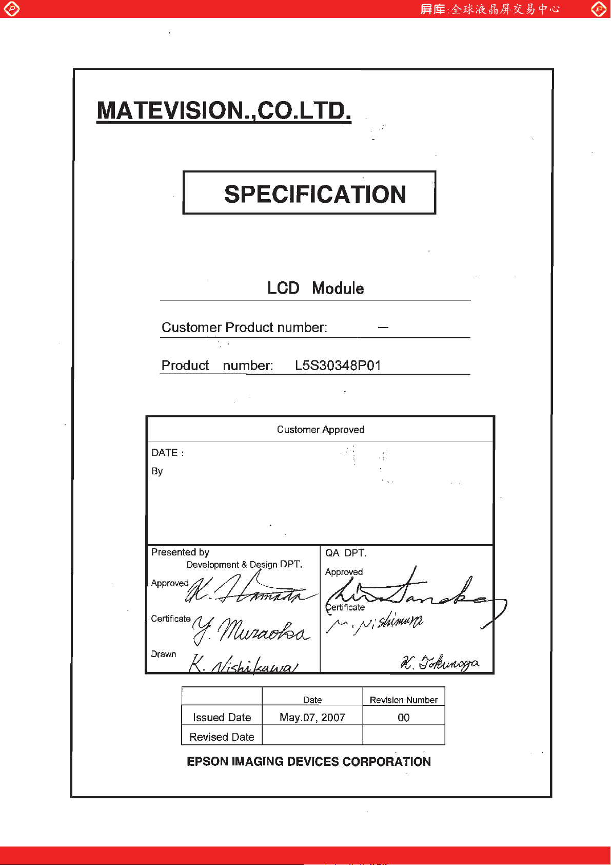
Global LCD Panel Exchange Center
www.panelook.com
One step solution for LCD / PDP / OLED panel application: Datasheet, inventory and accessory!
www.panelook.com
Page 2
Global LCD Panel Exchange Center
Product Number Rev. Revised item Date
L5S30348P01 00
www.panelook.com
REVISION HISTORY
Initial issue May. 07, 2007
QA STD Number
One step solution for LCD / PDP / OLED panel application: Datasheet, inventory and accessory!
www.panelook.com
Page 3
Global LCD Panel Exchange Center
www.panelook.com
Product Number L5S30348P01 Revision Number 00
Page 1/30
1. BASIC SPECIFICATIONS ................................................................................................................... 2
1.1 STRUCTURES ..................................................................................................................................................2
1.2 BLOCK DIAGRAM............................................................................................................................................3
1.3 I/O PINS ............................................................................................................................................................4
2. FUNCTIONS......................................................................................................................................... 5
2.1 OVERVIEW .......................................................................................................................................................5
2.1.1 Interface (LVDS) data assignment.......................................................................................................................5
2.1.2 Internal signals ....................................................................................................................................................5
2.1.3 Data and Color arrangement ...............................................................................................................................6
2.1.4 Data and Display Position....................................................................................................................................6
3. ABSOLUTE MAXIMUM RATINGS ......................................................................................................7
3.1 ELECTRICAL ABSOLUTE MAXIMUM RATINGS ........................................................................................... 7
3.2 ENVIRONMENTAL ABSOLUTE MAXIMUM RATINGS................................................................................... 7
4. ELECTRICAL SPECIFICATIONS........................................................................................................8
4.1 ELECTRICAL CHARACTERISTICS ................................................................................................................8
4.2 BACKLIGHT CHARACTERISTICS ..................................................................................................................9
4.3 TIMINGS..........................................................................................................................................................10
4.3.1 Interface ( LVDS ) signal timing parameteres ....................................................................................................10
4.3.2 Jitter tolerance ...................................................................................................................................................11
4.3.3 Interface signal timing parameters (DE MODE).................................................................................................12
4.3.4 Internal signals timing chart (DE MODE) ...........................................................................................................12
4.4 RECOMMENDED SEQUENCE ......................................................................................................................13
5. OPTICAL SPECIFICATION ............................................................................................................... 14
5.1 OPTICAL SPECIFICATION ............................................................................................................................14
5.2 DEFINITION AND CONDITION OF OPTICAL CHARACTERISTICS ............................................................15
6. INSPECTION...................................................................................................................................... 17
6.1QUALITY STANDARD .................................................................................................................................17
6.1.1 Standards ..........................................................................................................................................................17
6.1.2 Lot .....................................................................................................................................................................17
6.1.3 Inspection condition...........................................................................................................................................17
6.1.4 Treatment of defective products ........................................................................................................................17
6.1.5 Treatment of defective products in the acceptance inspection ..........................................................................17
6.1.6 Treatment of other problems .............................................................................................................................18
6.1.7 Warranty............................................................................................................................................................18
6.1.8 Applicable period of repair .................................................................................................................................18
6.2APPLICATION SCOPE ................................................................................................................................18
6.3DISPLAY APPEARANCE STANDARDS.....................................................................................................19
6.4EXTERNAL APPEARANCE STANDARDS.................................................................................................21
6.1 LABEL.............................................................................................................................................................22
6.1.1 Module label ......................................................................................................................................................22
6.1.2 Disposal label ....................................................................................................................................................22
6.1.3 Label position ....................................................................................................................................................22
7. DURABILITY...................................................................................................................................... 23
8. LCD MODULE USAGE AND PRECAUTIONS .................................................................................. 25
8.1 HANDLING......................................................................................................................................................25
8.2 DESIGN OF APPLICATION ...........................................................................................................................27
8.3 STORAGE....................................................................................................................................................... 29
8.4 DISPOSAL ......................................................................................................................................................30
8.5 OTHER PRECAUTIONS.................................................................................................................................30
OUTWARD DRAWINGS ................................................................................................ Attached sheet
EPSON IMAGING DEVICES CORP㧚
One step solution for LCD / PDP / OLED panel application: Datasheet, inventory and accessory!
www.panelook.com
Page 4
R
R
Global LCD Panel Exchange Center
www.panelook.com
Product Number L5S30348P01 Revision Number 00
1.BASIC SPECIFICATIONS
1.1 STRUCTURES
No. PARAMETER SPECIFICATIONS UNIT
1 LCD structure
2 Outward
3 Weight 465 Typ. g
4 Active area [Screen dimension]
5 Bezel opening area
6 Number of dots
7 Dot pitch
8 Dot layout Vertical stripe -
9 Viewing direction 6 o’clock 10 Liquid crystal mode TN, Normally white, Transmissive type 11 Polarization plate Non-glare -
*1) See attached drawing for details.
Dot pitch
Dot
Pixel
G B
Dot
Dot pitch
TFT LCD -
284.0(W) x 215.6(H) x 6.8 Max. (T) mm
270.336(W) x 202.752(H) [13.3 inch] mm
273.6(W) x 206.0(H)
1024 x R·G·B(W) x 768(H) -
0.088(W) x 0.264(H) mm
Page 2/30
mm
EPSON IMAGING DEVICES CORP㧚
One step solution for LCD / PDP / OLED panel application: Datasheet, inventory and accessory!
www.panelook.com
Page 5
Global LCD Panel Exchange Center
www.panelook.com
Product Number L5S30348P01 Revision Number 00
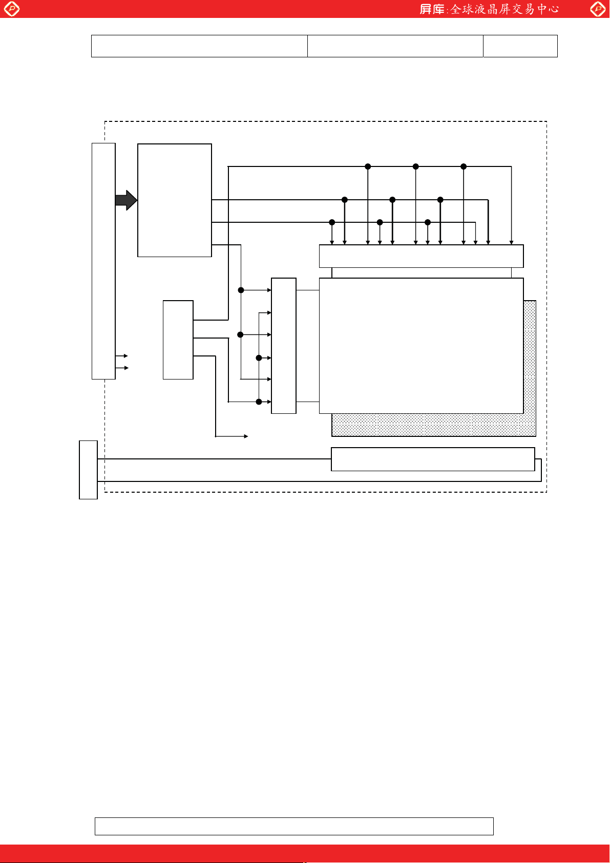
1.2 BLOCK DIAGRAM
CN1
VDD
VSS
FLCN 1
NOTE 1) This model is not equipped with an inverter circuit.
ASIC
TFT
Timing
Controller
(LVDS-Receiver)
DC/DC
Converter
DATA
Vcom
Gate Driver
768
Page 3/30
Source Driver
1024u(RGB)
TFT Panel
Back Light
CFL
EPSON IMAGING DEVICES CORP㧚
One step solution for LCD / PDP / OLED panel application: Datasheet, inventory and accessory!
www.panelook.com
Page 6
Global LCD Panel Exchange Center
www.panelook.com
Product Number L5S30348P01 Revision Number 00
1.3 I/O PINS
LCM㧦CN1
PIN NO. SYMBOL FUNCTION
1 VDD Power Supply ( 3.3V +/- 0.3V)
2 VDD Power Supply ( 3.3V +/- 0.3V)
3 VSS Ground
4 VSS Ground
5 Rin0- LVDS Differential data input (-)
6 Rin0+ LVDS Differential data input (+)
7 VSS Ground
8 Rin1- LVDS Differential data input (-)
9 Rin1+ LVDS Differential data input (+)
10 VSS Ground
11 Rin2- LVDS Differential data input (-)
12 Rin2+ LVDS Differential data input (+)
13 VSS Ground
14 RCLK- LVDS Differential Clock input (-)
15 RCLK+ LVDS Differential Clock input (+)
16 VSS Ground
17 NC No Connection䋨Should be opened during operation䋩
18 NC No Connection䋨Should be opened during operation䋩
19 VSS Ground
20 VSS Ground
Page 4/30
I/O REMARKS
P
P
P
P
I
I
P
I
I
P
I
I
P
I
I
P
-
P
P
CN1: DF19KR-20P-1H (HIROSE)
Suitable mating connector : DF19G-20S-1C (HIROSE) Wire type
㧦DF19G-20S-1F (HIROSE) FPC type
I/O : Input / Output terminal, I : Input terminal, O : Output terminal, P : Power line terminal
NOTE 1) Internal termination resistors of LVDS input lines are 100 ohms.
NOTE 2)
Valid synchronous signals are DCLK and DE. HSYNC and VSYNC are not used.
Backlight : FLCN1
PIN NO. SYMBOL FUNCTION
1 H.V High voltage for CFL
2 LGND Low voltage for CFL
I/O REMARKS
P
P
FLCN1 : BHSR-02VS-1 (JST)
Suitable mating connector: SM02B–BHSS-1-TB (JST)
NOTE 1) I/O : Input / Output terminal, I : Input terminal, O : Output terminal, P : Power line terminal
EPSON IMAGING DEVICES CORP㧚
One step solution for LCD / PDP / OLED panel application: Datasheet, inventory and accessory!
www.panelook.com
Page 7
R
4
R
3
R
2
R
0
0 (
5
(
)
0
4
9
3
2
8
7
6
5
Global LCD Panel Exchange Center
www.panelook.com
Product Number L5S30348P01 Revision Number 00
2. FUNCTIONS
2.1OVERVIEW
2.1.1 Interface (LVDS) data assignment
Rin0 +/-
Rin1 +/-
Rin2 +/-
RCLK +/-
Rxout 6
G0 (LSB)
Rxout 13
B1
Rxout 20
DE
R5(MSB)
Rxout 12
B
Rxout 19
VSYNC
Rxout 5
LSB)
xout
R4
Rxout 11
G
MSB
Rxout 1
HSYNC
xout
R3
Rxout 1
G
Rxout 1
B5(MSB)
xout
R2
Rxout
G
Rxout 1
B4
xout 1
R1
Rxout 8
G
Rxout 1
B3
Rxout
R0 (LSB)
Rxout 7
G1
Rxout 14
B2
Page 5/30
2.1.2 Internal signals
SYMBOL FUNCTION
DCLK Data Clock
HSYNC Horizontal Sync. (This signal is invalid.)
VSYNC Vertical Sync. (This signal is invalid.)
DE Data Enable (positive)
R0 Red Data (LSB)
R1 Red Data
R2 Red Data
R3 Red Data
R4
R5
Red Data
Red Data (MSB)
G0 Green Data (LSB)
G1 Green Data
G2 Green Data
G3 Green Data
G4 Green Data
G5 Green Data(MSB)
B0 Blue Data (LSB)
B1 Blue Data
B2 Blue Data
B3 Blue Data
B4
B5
Blue Data
Blue Data (MSB)
NOTE 1) “DE mode “ only.
The valid synchronous signals are DCLK and DE. HSYNC and VSYNC are invalid.
NOTE 2) INTERNAL SIGNALS are loaded from LVDS - Receiver to TFT Timing controller
with LVDS sequence. (See BLOCK DIAGRAM.)
EPSON IMAGING DEVICES CORP㧚
One step solution for LCD / PDP / OLED panel application: Datasheet, inventory and accessory!
www.panelook.com
Page 8
Global LCD Panel Exchange Center
www.panelook.com
Product Number L5S30348P01 Revision Number 00
2.1.3 Data and Color arrangement
INPUT DATA
DISPLAY
COLOR
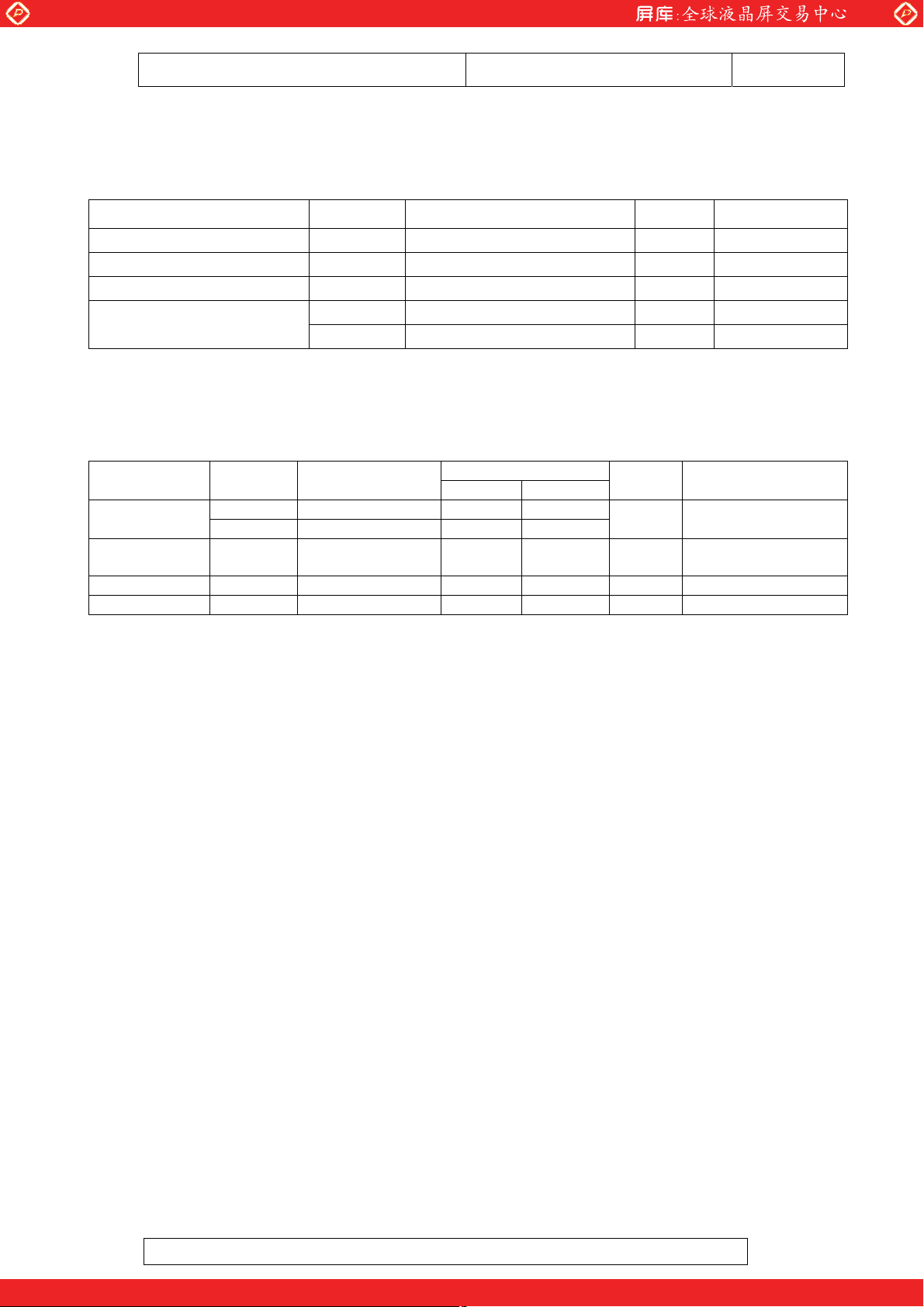
BLACK L L L L L L L L L L L L L L L L L L
RED H H H H H H L L L L L L L L L L L L
GREEN L L L L L L H H H H H H L L L L L L
BASIC
COLOR
BLUE L L L L L L L L L L L L H H H H H H
CYAN L L L L L L H H H H H H H H H H H H
MAGENTA H H H H H H L L L L L L H H H H H H
YELLOW H H H H H H H H H H H H L L L L L L
WHITE
BLACK L L L L L L L L L L L L L L L L L L
RED(1) L L L L L H L L L L L L L L L L L L
RED(2) L L L L H L L L L L L L L L L L L L
RED
: : : :
: : : :
RED(61) H H H H 䌌 HLLLLLLL L L LLL
RED(62) H H H H H 䌌 LLLLLLL L L LLL
RED(63)
BLACK L L L LLLLLLLLLL L L LLL
GREEN(1) L L L LLLLLLLLHL L L LLL
GREEN(2) L L L LLLLLLL䌈䌌L L L L L L
GREEN
: : : :
: : : :
GREEN(61) L L L L L L H H H 䌈䌌H L L L L L L
GREEN(62) L L L L L LHHHHH䌌 L L L L L L
GREEN(63)
BLACK L L L LLLLLLLLLL L L LLL
BLUE(1) L L L LLLLLLLLLL L L LLH
BLUE(2) L L L LLLLLLLLLL L L LHL
BLUE
: : : :
: : : :
BLUE(61) L L L LLLLLLLLLH H H H䌌䌈
BLUE(62) L L L LLLLLLLLLH H H HH䌌
BLUE(63)
Page 6/30
RED DATA
MSB LSB MSB LSB MSB LSB
R5 R4 R3 R2 R1 R0 G5 G4 G3 G2 G1 G0 B5 B4 B3 B2 B1 B0
H H H H H H H H H H H H H H H H H H
H H H H H H L L L L L L L L L L L L
L L L L L L HHHH䌈䌈L L L L L L
L L L LLLLLLLLLH H H HHH
GREEN DATA BLUE DATA
NOTE 1) Chromaticity (n) --- "n" indicates grayscale's number.
2.1.4 Data and Display Position
1㨯1 1㨯2
2㨯1
.
.
.
.
767㨯1
768㨯1 768㨯2
VpHp R G B
. . . . . . . .
. . . . . . . . .
EPSON IMAGING DEVICES CORP㧚
1㨯1023 1㨯1024
2㨯1024
.
.
.
.
767㨯1024
768㨯1023 768㨯1024
One step solution for LCD / PDP / OLED panel application: Datasheet, inventory and accessory!
www.panelook.com
Page 9
Global LCD Panel Exchange Center
www.panelook.com
Product Number L5S30348P01 Revision Number 00
Page 7/30
3. ABSOLUTE MAXIMUM RATINGS
3.1 ELECTRICAL ABSOLUTE MAXIMUM RATINGS
Ta= 25 deg C
PARAMETER SYMBOL RATINGS UNIT REMARKS
Power supply voltage VDD-VSS 4.0 V
LVDS Input voltage VIN
CFL current IL 7.0 mA
VHV 2000 Vrms CFL supply voltage
V
LGND 100 Vrms
NOTE 1)㩷 VIN: Rin0-/+, Rin1-/+, Rin2-/+, RCLK-/+
3.2 ENVIRONMENTAL ABSOLUTE MAXIMUM RATINGS
PARAMETER SYMBOL CONDITIONS
TST Storage -20 60 Ambient
temperature
OP Operation 0 50
T
Humidity - Ta=40 deg C
max.
Vibration - Storage - 1.5 G NOTE 3)
Shock - Storage - 50 G XYZ 6ms / direction
VSS – 0.3 㨪 VDD + 0.3
RATINGS
MIN MAX
- 85 %RH No condensation
V NOTE 1)
Ta= 25 deg C
UNIT REMARKS
deg.C NOTE 1)
NOTE 2)
NOTE 1) Care should be taken so that the LCD module may not be subjected to the temperature
beyond this specification
NOTE 2) Ta> 40 deg. C : Absolute humidity must be less than 85% RH/40 deg.C
NOTE 3) 10-200Hz, 30min/cycle, X/Y/Z each one cycle and except for resonant frequency.
EPSON IMAGING DEVICES CORP㧚
One step solution for LCD / PDP / OLED panel application: Datasheet, inventory and accessory!
www.panelook.com
Page 10
Global LCD Panel Exchange Center
www.panelook.com
Product Number L5S30348P01 Revision Number 00
4. ELECTRICAL SPECIFICATIONS
4.1 ELECTRICAL CHARACTERISTICS
VDD =3.3V , fCLK = 65MHZ, fH = 48.4kHz, fV = 60Hz, Ta = 25 deg C
PARAMETER SYMBOL CONDITIONS
MIN TYP MAX
Power supply voltage VDD-VSS
LVDS input Threshold
voltage
Common mode voltage
of LVDS input
VTH
VTL
CM
V
High level - - +100
Low level -100 - -
1.125 1.25 1.375 V
Power supply current IDD NOTE 1) - 250 - mA
NOTE 1) Display pattern of Typ. value is 64 grayscales.
NOTE 2) V
CM : Common mode voltage of LVDS input.
< 64 grayscales >
RATINGS
3.0 3.3 3.6 V
Page 8/30
Unit REMARKS
Terminal
Post
CM=1.25V
mV
V
NOTE 2)
EPSON IMAGING DEVICES CORP㧚
One step solution for LCD / PDP / OLED panel application: Datasheet, inventory and accessory!
www.panelook.com
Page 11
Global LCD Panel Exchange Center
www.panelook.com
Product Number L5S30348P01 Revision Number 00
Page 9/30
4.2 BACKLIGHT CHARACTERISTICS
Ta= 25 deg.C
PARAMETER
SYMBOL CONDITIONS
MIN TYP MAX UNIT REMARKS
CFL voltage VL - 630 - Vrms at IL=6.0mArms
CFL current IL 3.0 - 6.5 mArms
Driving frequency fL 40 - 65 kHz
Discharge starting
voltage
CFL lifetime
S - - 1350 Vrms at Ta=0 degC
V
tOL
20000
- - Hours
at I
L=6.0 mArms
continuous
operating
NOTE 5)
NOTE 1) There may be a display flickering by interaction of the backlight driving conditions
(especially for the Inverter frequency f
L) and the module's horizontal frequency fH.
Therefore, sufficient confirmation should be made when using inverter.
NOTE 2) The open circuit voltage of the Inverter should be designed higher than the discharge
starting voltage recorded in this table, and also should be applied more than 1 second. If
not applied as mentioned above, the backlight may not start properly.
NOTE 3) Asymmetrical waveform will cause a degradation of lifetime by unevenness of mercury.
Therefore, the current waveform should have an unbalancing-ratio of less than 10%, and
an amplitude-ratio of less than 2 ±10%. The current waveform should be measured by
actual final product.
Ip
-p
I
Current Waveform
Unbalance rate = | Ip - I-p | / IL x 100 (%)
Wave-height rate = I
p (or I-p) / IL
p :High peak
I
-p :Low peak
I
L :RMS
I
NOTE 4) Be sure to use a Ground Referenced type for the Inverter. Don't use a Ground Floating
type.
NOTE 5) The value that corresponds to the items written below is the definition of CFL life (when the
CFL is lit at Ta= 25, IL= 6.0mA):
1) when the brightness of the CFL falls to 50% or less of its initial value,
2) when the lighting start voltage does not fulfill the value written above
NOTE 6) The regulation of the CFL life is when the direction of the CFL tube axis (longer length of the
LCD module) is installed horizontally in the module. The life of the CFL may shorten when
the LCD module is used vertically due to mercury migration within the CFL tube.
NOTE 7) The CFL life will differ depending on the environmental temperature the LCD module is
used in. If the CFL is used in a cold/ hot environment for a long period of time, the
brightness will decrease drastically which may lead to a shorter CFL life.
EPSON IMAGING DEVICES CORP㧚
One step solution for LCD / PDP / OLED panel application: Datasheet, inventory and accessory!
www.panelook.com
Page 12
Global LCD Panel Exchange Center
www.panelook.com
Product Number L5S30348P01 Revision Number 00
4.3TIMINGS
4.3.1 Interface ( LVDS ) signal timing parameteres
VDD = 3.3V , fCLK = 65MHz , Ta = 25 deg.C
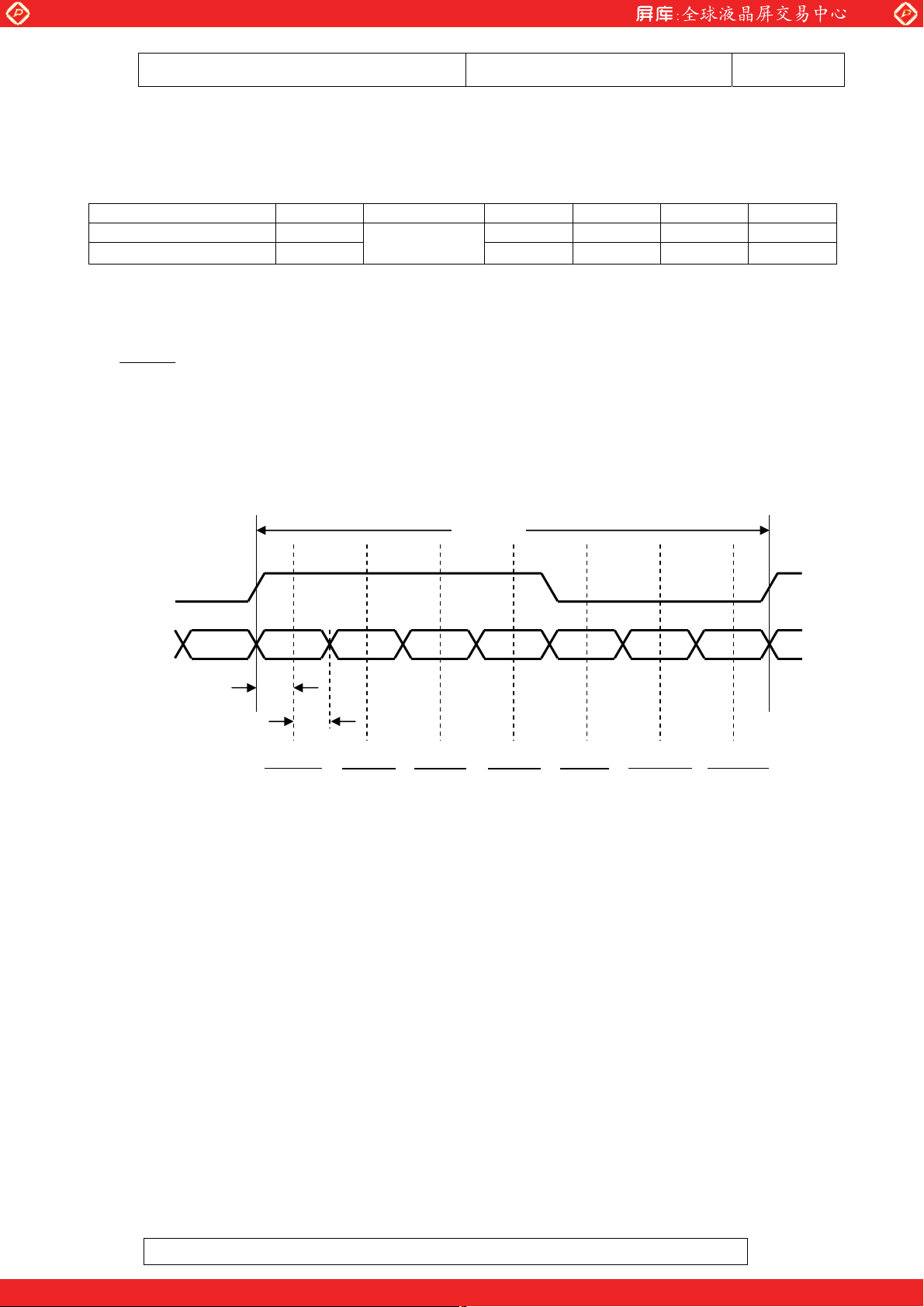
PARAMETER SYMBOL
Data setup time tsu 420 - - ps
Data hold time thd
CONDITION MIN TYP MAX UNIT
t
CLK=15.4ns
420 - - ps
The timing waveform in Figure 1 indicates the ideal strobe point of the LVDS input data:
n · tCLK
n : odd number
14
t
CLK : LVDS input clock period
The data setup time is "tsu" and the data hold time is "thd".
14
tCLK
7 tCLK
14
9 tCLK
14
11 tCLK
14
13 tCLK
RCLK +/-
Rin x +/-
㩷 tsu
thd
1 tCLK
14
Figure 1. LVDS data-input-timing waveform diagram
3 tCLK
14
5 tCLK
Page 10/30
14
EPSON IMAGING DEVICES CORP㧚
One step solution for LCD / PDP / OLED panel application: Datasheet, inventory and accessory!
www.panelook.com
Page 13

p
Global LCD Panel Exchange Center
www.panelook.com
Product Number L5S30348P01 Revision Number 00
4.3.2 Jitter tolerance
PARAMETER SYMBOL
MIN TYP MAX UNIT
Simple cycle jitter tcj1 - - 300 ps
Clock-period change rate tcj2 - - 25 ps / cycle
period (ns)
LVDS in
25.4
25.3
25.2
25.1
25.0
ut clock cycle Jitter example
24.9
24.8
0 50 100 150
cycle
Page 11/30
Figure 2 Example of impermissible cycle jitter
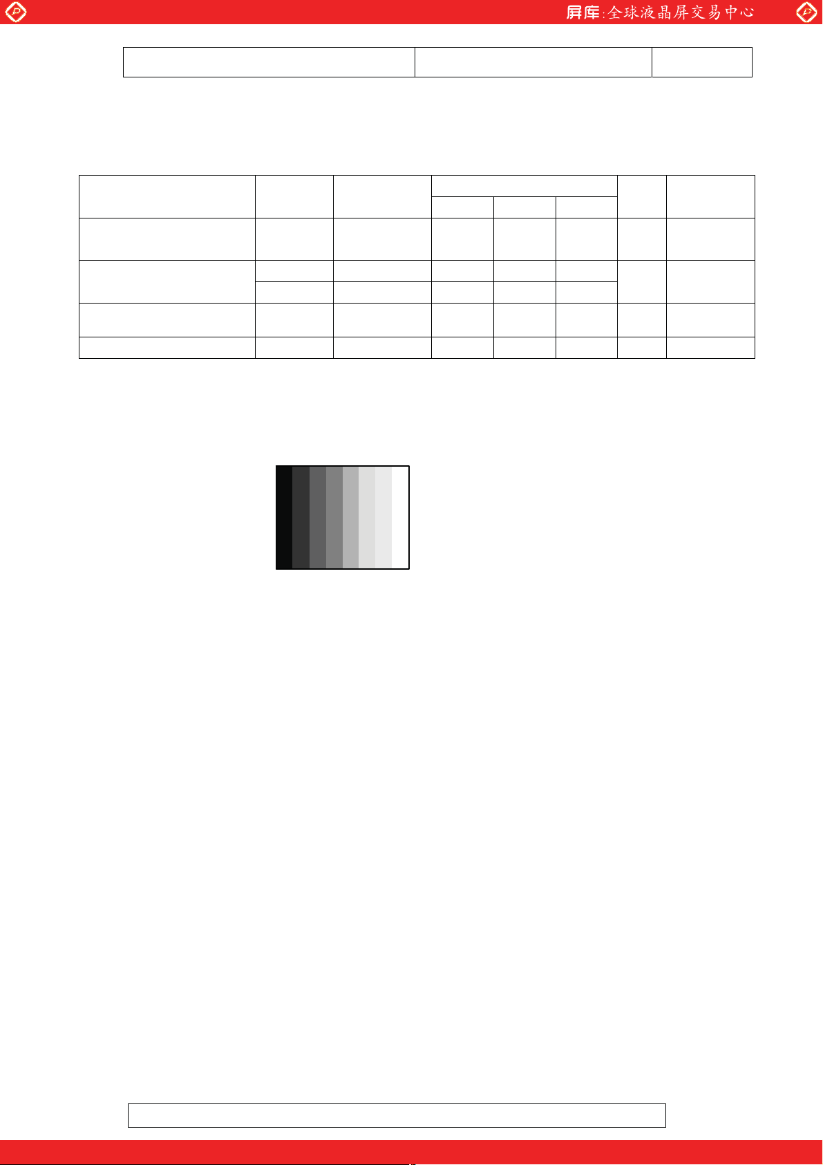
Assuming that the period of a given clock cycle "n" is represented by "tCLK", for example, the period
of cycle "n + 1" may be tolerated up to t
CLK ± 300 [ps]. However, if period fluctuations continue, the
limit to that change rate, rather than this tolerable range, constitutes the "clock-period change rate."
For 28 to 32 cycles in Figure 2, the lowest clock period during this interval is 24.9 [ns], and the
highest clock period is 25.3 [ns].
25.3 - 24.9 = 0.4 [ns]
0.4 / 5 (cycles) = 0.08 [ns]
Because a period fluctuation of 80 [ps] per cycle exists here, the rated "clock-period change rate" in
the above table is not achieved.
EPSON IMAGING DEVICES CORP㧚
One step solution for LCD / PDP / OLED panel application: Datasheet, inventory and accessory!
www.panelook.com
Page 14

Global LCD Panel Exchange Center
www.panelook.com
Product Number L5S30348P01 Revision Number 00
Page 12/30
4.3.3
Interface signal timing parameters (DE MODE)
PARAMETER SYMBOL MIN TYP MAX UNIT REMARKS
Clock Frequency fCLK 60.0 65.0 66.6 MHz (fCLK=1/tCLK)
Horiz. Period tHP 1270 1344 1450 tCLK
Horiz. DE tHDE 1024 1024 1024 tCLK
Horiz. Frequency fH 44.6 48.4 49.5 KHz (fH=1/tHP)
Vert. Period tVP 780 806 900 tHP fV=60Hz typical
Vert. DE nVDE 768 768 768 tHP
Vert. Frequency fV 55 60 62 Hz fV=1/tVP
NOTE 1) These signal timing parameters are specified at the digital inputs of LVDS transmitter.
With respect to setup time and hold time for DE and DATA signals, please refer to input
signal specification of LVDS transmitter.
Recommended LVDS transmitter : SN75LVDS84 (TI)
NOTE 2) Values recorded in this table indicate the properly operating conditions of the internal logical
functions. They don't guarantee the display quality or the display situation.
4.3.4
Internal signals timing chart (DE MODE)
DE
DE
Shrink
HP
t
tHDE
tVP
1 2 - - - - - n-1 n
n
VDE
EPSON IMAGING DEVICES CORP㧚
One step solution for LCD / PDP / OLED panel application: Datasheet, inventory and accessory!
www.panelook.com
Page 15

Global LCD Panel Exchange Center
www.panelook.com
Product Number L5S30348P01 Revision Number 00
4.4 RECOMMENDED SEQUENCE
VDD
LVDS
CFL
(Recommend)
0< t1< 25ms
0V
0V
0 < t
ON
OFF
10%
2< 65ms
100ms < t3
Power-on
90%
5ms < t6< 200ms
5 < 50ms
0 < t
VALID DATA
Power-off
90%
VTH
VTL
0ms < t
10%
VCM
4
Page 13/30
150ms < t
VDD=3.3V
7
NOTE 1) LVDS input should be set to "L" level or "Hi-Z.", when the power is turned off.
NOTE 2) LVDS input should be set to "L" level or "H" level, when the power is turned on. Don't set
them to "Hi-Z."
NOTE 3) Although no sequence for CFL is specified here, properly maintained timing is
recommended as described above. If the backlight is turned on before or after the LVDS
signal input, the display may be disordered by the changing of the LCD signals from the
timing controller (included in this module). Liquid crystal material or driving circuit can not
be damaged by the disorder of the display.
EPSON IMAGING DEVICES CORP㧚
One step solution for LCD / PDP / OLED panel application: Datasheet, inventory and accessory!
www.panelook.com
Page 16

Global LCD Panel Exchange Center
www.panelook.com
Product Number L5S30348P01 Revision Number 00
5. OPTICAL SPECIFICATION
5.1 OPTICAL SPECIFICATION
VDD = 3.3V, fCLK = 65MHZ, fH = 48.4kHz, fV = 60Hz, Ta = 25deg.C
PARAMETER CONDITIONS SYMBOL
Contrast ratio
RED - x
RED - y
GREEN - x
Display Color
Response
GREEN - y
BLUE - x
BLUE - y
WHITE - x
WHITE - y
B -> W
W -> B
Brightness
Brightness uniformity
Viewing angle CR>10
T= 0 deg.
T= 0 deg.
T= 0 deg.
T= 0 deg.
T= 0 deg. GB
Page 14/30
RATINGS
MIN. TYP. MAX.
UNIT
CR 300 500 - - NOTE)2,4,7
Rx 0.56 0.59 0.62
Ry 0.32 0.35 0.38
Gx 0.29 0.32 0.35
Gy 0.53 0.56 0.59
Bx 0.12 0.15 0.18
By 0.08 0.11 0.14
Wx 0.285 0.315 0.345
Wy
tr - 20 -
tf - 5 -
0.300 0.330 0.360
ms NOTE)3,4,7
B 380 480 - cd/m
- - 1.60 - NOTE)5,6,7
B 30 45 R 40 50 T 10 25 -
deg.
L 40 50 -
DEFINITION
- NOTE)4,7
2
NOTE)4,6,7
NOTE)
1, 2, 4,7
EPSON IMAGING DEVICES CORP㧚
One step solution for LCD / PDP / OLED panel application: Datasheet, inventory and accessory!
www.panelook.com
Page 17

g
Global LCD Panel Exchange Center
www.panelook.com
Product Number L5S30348P01 Revision Number 00
5.2 DEFINITION AND CONDITION OF OPTICAL CHARACTERISTICS
Display face
Left
TB
Normal(T=0deg.)
TL
TR
TT
Top
BLACK
WHITE DATA
100%
B
90%
Bottom
10%
0%
VT
Ri
ht
NOTE1) Viewing Angle NOTE3) Response:
NOTE2) Contrast ratio "CR"
Page 15/30
BLACK
VH
White brightness
CR =
Black brightness
NOTE 4) Measured at the center of the active area ( point 3 in NOTE 6 )
NOTE 5) Brightness uniformity "GB "
GB=
Maximum brightness of the 5points
Minimum brightness of the 5points
EPSON IMAGING DEVICES CORP㧚
One step solution for LCD / PDP / OLED panel application: Datasheet, inventory and accessory!
www.panelook.com
Page 18

p
p
p
p
Global LCD Panel Exchange Center
www.panelook.com
Product Number L5S30348P01 Revision Number 00
NOTE 6) Measurement points
1/6Vp
1/2V
5/6V
NOTE 7) Measuring conditions
(1) Instrument : BM-5A (TOPCON Corp.), Field= 2 degree
(2) Measurement distance : 50 cm
(3) Ambient temperature Ta : 25±2
(4) Display : White screen, Red screen, Green screen, Blue Screen, Black Screen
(5) Display : V
(6) Measuring after 30min. elapsed from CFL starting on.
(7) CFL tube current : IL= 6.0 mArms
CFL Inverter : CXA-L0612A-VJL (TDK)
1/6Hp
1/2H
1 2
5/6H
3
4
5
Vp: vertical pixel number
Hp: horizontal pixel number
deg C
DD = 3.3V, fCLK = 65MHz, fH = 48.4kHz, fV = 60Hz
Page 16/30
Active area
EPSON IMAGING DEVICES CORP㧚
One step solution for LCD / PDP / OLED panel application: Datasheet, inventory and accessory!
www.panelook.com
Page 19

Global LCD Panel Exchange Center
www.panelook.com
Product Number L5S30348P01 Revision Number 00
6. INSPECTION
6.1QUALITY STANDARD
6.1.1 Standards
The standards are the quality level used to judge whether or not product lots pass during acceptance
inspections of products delivered to your company. The standards are shown below.
Inspection method: Compliant with ANSI/ASQC Z1.4-1993, ordinary inspection level Τ, inspection
by one time sampling.
AQL
Defect type AQL Definition
Major defects 0.4% Accompanied with functional abnormalities
Minor defects 1.5% Out of the range of "6.3 EXTERNAL APPEARANCE STANDARDS", but
6.1.2
Lot
Page 17/30
no functional abnormalities
Lot means the unit includes all products delivered to your company at one time.
6.1.3
Inspection condition
(1) Environmental condition
Under 20 to 25deg.C, 60±15%RH.
Operative inspections are done under 800 to 2000 lx environment.
Especially related to transparence are performed under at most 50 lx environment.
(2) Inspection method
Inspect the screen by naked eye from a distance of about 30cm on a vertical direction front
on.
(3) Driving condition
According to the specification
6.1.4
Treatment of defective products
When defective products were found in your company's acceptance inspection and manufacturing
process or field, we treat them according to the rules below.
6.1.5
Treatment of defective products in the acceptance inspection
(1) When a product has failed to pass your company's acceptance inspection, please notify to
EPSON IMAGING DEVICES CORP. within 3 weeks from delivery. Otherwise, EPSON
IMAGING DEVICES CORP. will regard that it had been accepted.
(2) When a lot has failed to pass your company's acceptance inspection, please return the entire
lot to EPSON IMAGING DEVICES CORP. EPSON IMAGING DEVICES CORP. will investigate
the causes of defects and will report both the causes and the responses taken to them.
Non-defective products shall be delivered to replace all defective products within
nonconforming lots.
Non-defective products shall be delivered to replace all defective products within conforming lots.
(3)
EPSON IMAGING DEVICES CORP㧚
One step solution for LCD / PDP / OLED panel application: Datasheet, inventory and accessory!
www.panelook.com
Page 20

Global LCD Panel Exchange Center
www.panelook.com
Product Number L5S30348P01 Revision Number 00
6.1.6
Treatment of other problems
Page 18/30
If any troubles should occur concerns our products that have been assembled at your company's
manufacturing processes, both companies shall jointly investigate and resolve the causes.
6.1.7
Warranty
EPSON IMAGING DEVICES CORP. warrants this product for a period of 12 months from production
date indicated on the Lot Label attached to the product.
Warranty period for repaired products shall be 6 months from production date indicated on the repair
Lot Label attached to the product.㩷
During this period, supplier responsible failures shall be repaired free of charge.
6.1.8
Applicable period of repair
Applicable period of repair shall be 24months from production date indicated on the Lot Label
attached to the product.
After 24 months, we cannot provide you our repair service.
㩷㩷
6.2APPLICATION SCOPE
The application scope is limited to the viewing area.
The product should be judged non-defective if all defects are outside of the viewing area and do not
interfere with product quality or the assembly process.
Each "dot" means the smallest display unit for R, G or B.
A set of three adjacent R, G and B dots comprise one pixel.
EPSON IMAGING DEVICES CORP㧚
One step solution for LCD / PDP / OLED panel application: Datasheet, inventory and accessory!
www.panelook.com
Page 21

Global LCD Panel Exchange Center
www.panelook.com
Product Number L5S30348P01 Revision Number 00
Page 19/30
6.3DISPLAY APPEARANCE STANDARDS
If any item is defined with a boundary sample, the boundary sample takes precedence.
No. ITEM CRITERION CLASS
Display
1
problems
Missing lines No missing lines permitted. Major
2
Dot defects Defined allowable ranges should be met for each white, black, R, G, B
3
Inconsistent
4
display
Refuses and
5
scratches on
polarizer or
glass
*2)
Must not include any nonfunctioning or failure to display the correct
pattern corresponding to input signal.
raster.
The limits apply to the entire display area. *1)
Those visible through the 5% ND-Filter are to be considered bright
dot defects.
Bright spot in 60% or more of dot aperture is defined as a bright dot
defect, less than 60% is permitted.
Black spot in 60% or more of typical pixel aperture is defined as a
black dot defect, less than 60% is permitted.
Should not be prominent.
If necessary, boundary samples should be provided.
<Dot shape>
Allowable range
1. distinctly recognized
size d (mm) numbers
d҇0.2 permitted
0.2㧨d҇0.3 5
0.3㧨d҇0.5 2
2. blurred
size d (mm) numbers
d҇ 0.64 permitted
0.64㧨d҇1.50 2
1.50㧨d 0
Major
defect
defect
Minor
defect
Minor
defect
Minor
defect
Criterion is applied also to pin-holes.
Defects must not be crowded.
Distinctly recognized spot is the one which can be seen at raster
pattern.
Blurred spot is the one which can not be seen at raster pattern but
can be seen at gray scale pattern.
<Line shape>
1. Scratch
L: Length (mm) W: Width (mm) numbers
permitted W҇0.03 permitted
.҇5.0 0.03㧨W҇0.10 3
- 0.10㧨W allowed
2. Black and white lines
L: Length (mm) W: Width (mm) numbers
permitted W҇0.03 permitted
.҇1.0 0.03㧨W҇0.15 4
- 0.15㧨W allowed
Minor
defect
EPSON IMAGING DEVICES CORP㧚
One step solution for LCD / PDP / OLED panel application: Datasheet, inventory and accessory!
www.panelook.com
Page 22

Global LCD Panel Exchange Center
www.panelook.com
Product Number L5S30348P01 Revision Number 00
Page 20/30
No. ITEM CRITERION CLASS
Bubbles in
6
polarizer
(display area)
*2)
Allowable range
size d (mm) numbers
d҇0.2 permitted
0.2㧨d҇0.3 5
Minor
defect
0.3㧨d҇0.5 2
0.5㧨d 0
*1: dot defect's allowable range
No. Item Bright dot defect Black dot defect total
1 Defects counts 5 5
10
2 Combined defects 2 2
Adjacent 2 bright dots and 2 black dots are counted as one dot respectively.
Linked three or more dots: none
Defects must be at least 5mm apart from one another.
*2: outward of refuses, scratches and bubbles
Dot shape Line shape
d=(a+b)/2
a
L
b
Gentle curve Curved arch Multiple curves
L
L (a)
W
W (b)
W
W (b)
L (a)
Any defect outside the viewing area can be ignored.
When viewing with the naked eye, any bent or dot-shaped item must be measured and checked
according to the dot shape defect's standard.
Refer to the following examples of measurement methods.
EPSON IMAGING DEVICES CORP㧚
One step solution for LCD / PDP / OLED panel application: Datasheet, inventory and accessory!
www.panelook.com
Page 23

Global LCD Panel Exchange Center
www.panelook.com
Product Number L5S30348P01 Revision Number 00
Page 21/30
6.4EXTERNAL APPEARANCE STANDARDS
No. ITEM CRITERION CLASS
1 Different
Not permitted. Major defect
specifications
2 Missing parts All parts must be complete. Major defect
3 Damaged resist on
Copper patterns on FPC must not be visible. Minor defect
FPC
4 Circuit pattern Must not be peeled or separated from FPC. Major defect
5 Conductive
refuses
No solder refuses or solder balls easily moving.
Fixed conductive refuses over 0.2mmǾ are not permitted.
Minor defect
Should not be crowded.
(crowded: means gathering more than 5pcs within Ǿ=5mm㧕
6 Dirt Should not be prominent.
Minor defect
Dirt on backside is permitted.
7 Dirt or scratch on
Should not be prominent. Minor defect
interface pins
8 Plating Must not be peeled, no rust, no discoloration. Minor defect
9 Soldering Solder omissions are not permitted at any solder point.
Solder bridges are not permitted.
Cold soldering is not permitted.
10 Parts soldering There must be fillet
Major defect
Major defect
Minor defect
Minor defect
EPSON IMAGING DEVICES CORP㧚
One step solution for LCD / PDP / OLED panel application: Datasheet, inventory and accessory!
www.panelook.com
Page 24

Global LCD Panel Exchange Center
www.panelook.com
Product Number L5S30348P01 Revision Number 00
7. PACKING
7.1 LABEL
7.1.1 Module label
L5S30348P01
***********7507
******************
7.1.2 Disposal label
COLD CATHODE FLUORESCENT LAMP IN LCD PANEL CONTAINS A SMALL AMOUNT OF MERCURY.
PLEASE FOLLOW LOCAL ORDINANCES OR REGULATION FOR DISPOSAL.
TFT-LCM
MADE IN JAPAN
(engraved)
EPSON Imaging Devices’s Product number
Module Lot No.
The last 4 digits indicate a production date.
(Ex.) May.07.2007
Panel Lot No.
Production country
Page 22/30
Production Month
Month : Code Month : Code
Jan. : 1 Jul. : 7
Feb. : 2 Aug. : 8
Mar. : 3 Sep. : 9
Apr. : 4 Oct. : X
May : 5 Nov. : Y
Jun. : 6 Dec. : Z
7.1.3 Label position
Module Label
Disposal Label (engraved)
EPSON IMAGING DEVICES CORP㧚
One step solution for LCD / PDP / OLED panel application: Datasheet, inventory and accessory!
www.panelook.com
Page 25

Global LCD Panel Exchange Center
www.panelook.com
Product Number L5S30348P01 Revision Number 00
8. DURABILITY
Reliability Test Item and Test Condition / Method
No. ITEMS CONDITION
1 Continuous operating test
at high temperature
2 Continuous operating test
at low temperature
3 Storage test at high
temperature
4 Storage test at low
temperature
5 Continuous operating test
at high temperature and
high humidity
6 Thermal shock test Hold the cycle test 120 times on the condition as follows :
7 Vibration test
(non-operating)
8 Shock test
(non-operating)
9 Electrostatic discharge test
(non-operating)
10 Shock test
(after packing)
11 Falling test
(after packing)
Apply rated voltage in an atmosphere of 50 ± 2 C and operate
240 hours.
Apply rated voltage in an atmosphere of 0 ± 2 C and operate 240
hours.
After allowing to stand for 240 hours at 60 ± 2 C, leave for 2 hours
at the room temperature and humidity for checking.
After allowing to stand for 240 hours at -20 C, leave for 2 hours at
the room temperature and humidity for checking.
After allowing to stand for 120 hours at 40 ± 2 C and 85% RH of
rela-tive humidity, leave for 2 hours at the room temperature and
humidity for checking.
Hold the cycle test 1 times in the direction of X, Y, Z respectively
on the condition as follows :
Vibration frequency : 10 ~ 200 Hz
Sweep : 30 min.
Acceleration : 1.5 G
Shock test condition is as follows :
Give the test on the condition as follows :
Give the air discharges at the center of the glass and 4 points on
the Bezel at each side, every 3 times.
Vibration frequency : 10 ~ 50 Hz
Acceleration : 1.0 G (Z direction) , 0.7G (XY direction)
Sweep : (10 ~ 50 Hz)/10 min
Repetition : 1 time
Direction : ±XYZ
Figure 1 shows fall parts.
It falls so that parts in Figure 1(A ~ F) may collide with floor.
(It falls in alphabetical order)
Table 1 shows height of fall.
-20 ± 2 C : 60 minutes
60 ± 2 C : 60 minutes
Acceleration : 50 G
Acting time : 6 ms
Direction : ±XYZ
Capacity : 200 / 100
Resistance : 0 / 1.5
machine model / human body model
pF
k
Applied voltage : ± 7.5 kV
Page 23/30
EPSON IMAGING DEVICES CORP㧚
One step solution for LCD / PDP / OLED panel application: Datasheet, inventory and accessory!
www.panelook.com
Page 26

Global LCD Panel Exchange Center
www.panelook.com
Product Number L5S30348P01 Revision Number 00
Surface H
Surface G
Angle D
Edge A
Figure 1
Edge B
Surface F
Surface E
Angle C
Page 24/30
Table 1
Part A B C D E F G H
Height of
80 80 80 80 100 100 100 100
Falling (cm)
EPSON IMAGING DEVICES CORP㧚
One step solution for LCD / PDP / OLED panel application: Datasheet, inventory and accessory!
www.panelook.com
Page 27

Global LCD Panel Exchange Center
www.panelook.com
Product Number L5S30348P01 Revision Number 00
9. LCD MODULE USAGE AND PRECAUTIONS
9.1 HANDLING
1) Broken glass:
Be careful to broken glass of display face. When display face is damaged, please be careful
enough not to cut hands by a piece of glass. The surface of a LCD module is covered by plastic
film, and glass is hard to be scattered, but there can be the hurt when touching a broken portion.
And because CFL is also made of glass, please be careful equally.
2) Broken panel:
Do not touch the liquid which flowed out of a panel. When a panel was damaged and the liquid flow,
don't breathe in the liquid, drink it, and touch it. When the liquid stuck to a hand or clothes, wipe it
off in soap or alcohol immediately, then wash in water. When the liquid touched to eyes, wash eyes
with washing water more than 15 minutes, and undergo a medical treatment of a doctor.
3) Preventing of stain and dust:
Handle a LCD module as much as possible in a room with a few dusts. In addition, when in
acceptance inspection or installing process, wear a finger case or the soft gloves which do not
make a dust to prevent stain of display face of a module.
4) Protection board of display face:
Remove a protection board of display face as later as possible in assembling process to prevent
dust or scratch onto display face.
5) Wiping off of stain on display face:
When display face of a LCD module was stained, please wipe it off lightly with cotton or soft clean
cloth. When even they are not removed, wipe it off lightly with cotton or soft clean cloth which
soaked with water. Be careful that water does not flow into the LCD module inside.
6) Water drops on display face:
Don't leave display face with water drops on. When water drops stuck, please wipe it off with cotton
or soft cloth immediately. Display face changes color and get a stain when leaving drops of water.
In addition, when water drops flow into the LCD module inside, there might cause a trouble.
7) Disassemble or modify of LCD module:
Do not attempt to disassemble, rework or modify the LCD module by any means. There is the
possibility of electric shock, destruction of electronic parts, scratch on a display face, or dust
passing into a LCD module. And if using disassembled, reworked or modified LCD module,
electronic parts might emit smoke or outbreak a fire by dust or malfunction of electronic parts. A
product guarantee becomes not available for a LCD module which disassembled, reworked or
modified by user.
Page 25/30
EPSON IMAGING DEVICES CORP㧚
One step solution for LCD / PDP / OLED panel application: Datasheet, inventory and accessory!
www.panelook.com
Page 28

Global LCD Panel Exchange Center
www.panelook.com
Product Number L5S30348P01 Revision Number 00
8) Countermeasures to static electricity:
C-MOS LSI and an electronic part of the LCD module inside can be destroyed by static electricity.
In order not to apply static electricity to a LCD module, spread a conductive mat to a floor and a
work desk. In addition, worker should mount a ground band. Make consideration to prevent of static
electricity while at work.
9) Inserting a CFL connector:
Insert a CFL connector justly. A connector for between a CFL power supply circuit and a CFL of a
LCD module incorporated backlight should not be inserted slantways or half-ways. And confirm it
by all means. When it is not inserted justly, a circuit and a part might emit smoke or be damaged by
burning by the high voltage of a CFL power supply circuit. In addition, when there is the possibility
that it is not inserted justly, be sure to insert a connector after having confirmed LCD module that
switched off a CFL power supply circuit. In addition, please does not use except a recommended
CFL connector.
10) Power supply when in a handling of LCD module:
Be careful to electric shocks. When handling a LCD module, do it after switching the power supply
off by all means. While in operation, there is the possibility of electric shocks by touching on a CFL
electrode, a cable, a connector, or a CFL power supply circuit, because the high voltage is applied.
11) Power supply in connecting operation:
Switch off the power supply of the parent application at the time of installing process by all means.
When inserting or pulling off a connector of a LCD module with having switched on the parent
application, it can be damaged in an electric circuit of a LCD module. When power supply have to
be turned on by testing or inspection process, use a driving circuit which satisfies the ON/OFF
sequence for power supply and input signals.
12) Heating-up of CFL circumference:
Warn a burn when operating backlight including a CFL. A CFL circumference becomes high
temperature.
13) How to insert a connector:
When inserting a cable in a connector of a LCD module or take it off, make attention so that strong
external force is not added to a connector of the LCD module. PWB and inside connection of a
TCP driver can be damaged by a strong external force. When installing a LCD module to a target,
make attention not to put these cables between the case of target and the LCD module. A
connector of a parent application and an input connector of LCD module should not be inserted
slantways or half-ways. And confirm it by all means. When it is not inserted justly, a circuit and a
part might emit smoke or be damaged by burning by the high voltage of a CFL power supply circuit.
14) Handling of a cable for backlight:
A CFL cable for backlight should not be pulled or damaged. They might cause troubles by the
damage of soldering on the root of a CFL or a CFL.
15) Immediately discontinue using the CFL when if it darkens drastically or turns pink because
depletion of effective mercury may be occurring within the CFL tube which may make the
temperature rise. Due to these characteristics, the CFL may break or generate smoke
Page 26/30
EPSON IMAGING DEVICES CORP㧚
One step solution for LCD / PDP / OLED panel application: Datasheet, inventory and accessory!
www.panelook.com
Page 29

Global LCD Panel Exchange Center
www.panelook.com
Product Number L5S30348P01 Revision Number 00
9.2 DESIGN OF APPLICATION
1) Absolute maximum ratings:
Follow the absolute maximum ratings specified in this document by all means. The absolute
maximum rating is the rating which LCD module must not be violated. When using a LCD module
at the condition beyond those, a burning / destruction of electronic parts or a permanent damage of
characteristics may be caused. Therefore, make appropriate design not to violate the absolute
maximum ratings with consideration of environmental temperature, deviation of input signals, and
electronic parts tolerances.
2) Polarity of power supply to a CFL:
Polarity of a CFL cable from CFL power supply should be designed as that the high voltage cable
and the low voltage cable cannot be assembled conversely. In addition, because there might be a
brightness degradation of backlight or a starting failure if the CFL cable is too long, do a design
becoming the cable shortest as much as possible.
3) Torsion and bending while in the process of installing:
Make sure that stresses, warps and twists are not applied to the LCD module when installing to a
target frame. Even if stresses are temporary, it may be the cause of failure to the LCD module.
4) Preventing of a mechanical shock:
Be careful not to give a strong mechanical shock such as drops or shocks. There can be a cause of
trouble such as a scratch of display face or a malfunction of LCD module.
5) Preventing of a pressure onto display face:
Make attention that no strong external force such as pushing strongly onto display face of a LCD
module. Because there can be a scratch on display face or a cause of trouble of a LCD module.
6) Preventing of a scratch on display face:
Make attention not to rub or push a display face of a LCD module by a rigid thing such as tools. In
addition, be sure not to put a heavy thing such as a tool on display face and not to pile up LCD
modules each other. A polarizer used for display face is easy to get a scratch or traces and it might
be damaged.
7) Preventing unevenness of the display:
EPSON Imaging Devices recommends use of all installation holes shown in this document. Screws
used should have proper dimensions according to the specifications. The housing case must be
designed carefully in order to prevent stresses, warps and curves on all directions of the LCD
module. If stresses, warps, and curves are applied to the LCD module, the display may turn out
uneven.
Page 27/30
EPSON IMAGING DEVICES CORP㧚
One step solution for LCD / PDP / OLED panel application: Datasheet, inventory and accessory!
www.panelook.com
Page 30

Global LCD Panel Exchange Center
www.panelook.com
Product Number L5S30348P01 Revision Number 00
8) Power supply of a CFL:
In the LCD module which backlight with CFL is incorporated in, be sure to design a CFL power
supply circuit to be able to be applied the open circuit voltage more than 1 second. If it is less than
it, there might be the possibility that a CFL does not turn on. In addition, a current control type
inverter should be used that can control a tube current. If using a voltage controlled type inverter,
excess current might flows in a high temperature environment, and, a starting characteristics of a
CFL may degrades in a low temperature environment.
In addition, please design the power supply of the backlight so that it would turn off quickly in the
following conditions:
a) when the LCD module turns dark or changes pink drastically,
b) when an overcurrent flows in the lamp cable,
c) when the inverter is unloaded
9) Countermeasures to heating-up:
When operating backlight with CFL, temperature in the target application which incorporated a LCD
module is raised. Therefore, give measures to radiate of heat such as holes of a case to satisfy
temperature specifications of a LCD module.
10) Noise of Power supply:
Because the spike noise existing in a power supply is a cause of malfunction of a driving circuit in a
LCD module or an abnormality of display, spike noise on VDD must be within 100 mV
violate the absolute maximum rating).
11) Power sequence:
Before LCD module is switched on, please make sure that power supply and input signals of
system, testing equipment, etc. meet the recommended power sequence. The protection circuit will
operate if the power supply sequence can not be kept and the LCD module may shut down.
12) Protection for power supply:
Please study to adapt protection for power supply against trouble of LCD module, depending on
usage condition of system. Fuse installed on LCD module should be never modified. Any
modification to make the function of fuse ineffective may cause burning or break of printed wiring
board or other components at circuit trouble.
13) Protection against electric shock
High voltage is applied to CFL connector, inverter circuit and CFL at lighting. Please make design
not to expose or be accessible to such high voltage parts to avoid electric shock.
14) Recommendation for use of a protection cover and a UV cut filter:
EPSON Imaging Devices recommends use of a transparent protection cover on a liquid crystal
display aperture to prevent scratch and dust of display face and invasion of water, when using
under a too cruel condition in such as outdoors. Furthermore, EPSON Imaging Devices
recommends use of a U.V. cut filter (cuts equal to or less than 390 nm) when it is exposed to direct
rays of the sun for a long time. Please consider it so that dew condensation does not occur in the
cover.
Page 28/30
P-P (but never
EPSON IMAGING DEVICES CORP㧚
One step solution for LCD / PDP / OLED panel application: Datasheet, inventory and accessory!
www.panelook.com
Page 31

Global LCD Panel Exchange Center
www.panelook.com
15) Temperature dependence of display:
The response (optical response) of display varies with temperature. The response becomes slow at
low temperature. In addition, brightness and chromaticity vary with temperature, too.
16) Starting delay and lifetime under low temperature:
The starting characteristic of a CFL degraded under low temperature (the time before light being
stable gets longer from power supply ON). In addition, please operate a CFL at room temperature
as possible, because the lifetime shortens when operating under low temperature by the
characteristics itself.
17) Dew condensation:
In an environment of sudden temperature change, there might be a dew condensation on surface
or inside of a LCD module. Because it causes a degradation of display or malfunction, be sure to
make consideration for design that dew condensation does not occur.
18) Image sticking:
19) Dirty and uneven display:
Dirt and unevenness sometimes partly appear with the increase in the total operation time.
20) Change of Color CIE coordinates:
When LCD module is used for a long time, the color of the parts in backlight changes, and it cause
the shift of the display color.
9.3 STORAGE
1) Storage and transport:
Keep a LCD module with a packing form of shipment in a dark room which direct rays of the sun
does not irradiate with low temperature, with low humidity, and with no dew condensation. In
addition, keep it in an environment with little temperature change because there is the possibility
that dew condensation occurs by a sudden temperature change. When dew condensation occurs, it
may be a cause of operation abnormality or trouble.
2) Transport:
Because the master carton may be damaged or shape transformed by an excessive load applied,
store and transport with piled up in lower than the number which recorded in a master carton label.
Product Number L5S30348P01 Revision Number 00
a) Image sticking may appear when the same pattern (still image, character etc.) have been
displayed for a long period of time.
b) When the LCD module is continuously displayed with a letterbox mode, Image sticking
may appear on the display.
We recommend that the LCD module is displayed with the full-screen mode in order to
prevent image sticking from occurring.
c) Image sticking normally disappears by displaying a gray-screen for a while. However
when the image sticking is remarkable, it may not disappear even if the gray screen is
displayed on the LCD module.
Page 29/30
EPSON IMAGING DEVICES CORP㧚
One step solution for LCD / PDP / OLED panel application: Datasheet, inventory and accessory!
www.panelook.com
Page 32

Global LCD Panel Exchange Center
www.panelook.com
Product Number L5S30348P01 Revision Number 00
3) Handling:
Because a LCD module is a product having precision electronic parts and glass products, it might
be damaged by an excessive shock or a dropping. Although a LCD module does protected with
master carton, handle it carefully to reduce a shock in transshipping, transporting and loading.
9.4 DISPOSAL
1) Disposing LCD modules:
When disposing LCD modules, consult a company specialized in industrial waste treatment which
is permitted by the government or the local authority. When disposing CFL, obey the regulations or
rules given by the local government because mercury is contained in the CFL.
9.5 OTHER PRECAUTIONS
1) This product is developed and produced to use for general electronic equipment (OA instrument
products, communication terminal instrument products, consumer electronics products, game
instrument products). The specifications does not correspond to a usage or a device that extremely
high reliability or safety are needed. ( i.e. aviation / space instruments, nuclear energy control
instruments, life-support equipment. )
2) Observe conditions and precautions in this document in use of this product. Even if in a range
of condition, use this product with considerations for safety design as a total system and instrument,
so that an accident resulting in injury, a fire accident, or the social damage will not occurs.
3) This product does not design as an anti-radiation device.
4) Any contents of this publication do not guarantee or approve the rights of enforcement for a
third person (party) about the intellectual property and others.
5) EPSON Imaging Devices forbids firmly modifying or copying a part or all of this publication
without a documented permission.
6) The contents stated in this document and the product may be subject to change without prior
notice.
When you kindly study to use product, please ask our distributor or us for the latest information.
Page 30/30
EPSON IMAGING DEVICES CORP㧚
One step solution for LCD / PDP / OLED panel application: Datasheet, inventory and accessory!
www.panelook.com
Page 33

q
Global LCD Panel Exchange Center
www.panelook.com
UNITmm
ue 0.20 N㨯m Max.
EPSON IMAGING DEVICES CORP. Product Number L5S30348P01 Rev. No. 00
OUTWARD DRAWINGS
One step solution for LCD / PDP / OLED panel application: Datasheet, inventory and accessory!
Note1 : Unspecified dimension tolerances are +/-0.5 mm
CN : DF19KR-20P-1H (HIROSE)
FLCN1 : BHSR-02VS-1(JST)
Note2 : Screw tor
www.panelook.com
Page 34

Global LCD Panel Exchange Center
www.panelook.com
One step solution for LCD / PDP / OLED panel application: Datasheet, inventory and accessory!
www.panelook.com
Page 35

Global LCD Panel Exchange Center
www.panelook.com
One step solution for LCD / PDP / OLED panel application: Datasheet, inventory and accessory!
www.panelook.com
Page 36

Global LCD Panel Exchange Center
www.panelook.com
One step solution for LCD / PDP / OLED panel application: Datasheet, inventory and accessory!
www.panelook.com
Page 37

Global LCD Panel Exchange Center
www.panelook.com
One step solution for LCD / PDP / OLED panel application: Datasheet, inventory and accessory!
www.panelook.com
Page 38

Global LCD Panel Exchange Center
www.panelook.com
One step solution for LCD / PDP / OLED panel application: Datasheet, inventory and accessory!
www.panelook.com
 Loading...