

Page 1
MF943-02
CMOS 4-BIT SINGLE CHIP MICROCOMPUTER
E0C6001 T
ECHNICAL
M
ANUAL
E0C6001 Technical Hardware
E0C6001 Technical Software
Page 2

NOTICE
No part of this material may be reproduced or duplicated in any form or by any means without the written
permission of Seiko Epson. Seiko Epson reserves the right to make changes to this material without notice.
Seiko Epson does not assume any liability of any kind arising out of any inaccuracies contained in this material
or due to its application or use in any product or circuit and, further, there is no representation that this material
is applicable to products requiring high level reliability, such as medical products. Moreover, no license to any
intellectual property rights is granted by implication or otherwise, and there is no representation or warranty that
anything made in accordance with this material will be free from any patent or copyright infringement of a third
party. This material or portions thereof may contain technology or the subject relating to strategic products under
the control of the Foreign Exchange and Foreign Trade Control Law of Japan and may require an export license
from the Ministry of International Trade and Industry or other approval from another government agency. Please
note that "E0C" is the new name for the old product "SMC". If "SMC" appears in other manuals understand that
it now reads "E0C".
© SEIKO EPSON CORPORATION 1998 All rights reserved.
Page 3

PREFACE
This manual is individualy described about the hardware and the software
of the E0C6001.
I. E0C6001 Technical Hardware
This part explains the function of the E0C6001, the circuit configurations, and details the controlling method.
II. E0C6001 Technical Software
This part explains the programming method of the E0C6001.
Hardware
Software
Page 4

Hardware
E0C6001
I.
Technical Hardware
Page 5

Hardware
CONTENTS
CHAPTER 1 INTRODUCTION............................................................... I-1
1.1 Configuration ................................................................... I-1
1.2 Features .......................................................................... I-2
1.3 Block Diagram ................................................................. I-3
1.4 Pin Layout Diagram......................................................... I-4
1.5 Pin Description ................................................................ I-5
CHAPTER 2 POWER SUPPLY AND INITIAL RESET ................................ I-6
2.1 Power Supply .................................................................. I-6
2.2 Initial Reset...................................................................... I-8
Oscillation detection circuit...................................... I-9
Reset pin (RESET) .................................................... I-9
Simultaneous high input to input ports (K00–K03) ... I-9
Internal register following initialization.................... I-10
2.3 Test Pin (TEST).............................................................. I-10
CHAPTER 3 CPU, ROM, RAM ............................................................ I-11
3.1 CPU................................................................................ I-11
3.2 ROM ............................................................................... I-12
3.3 RAM ............................................................................... I-12
Page 6

CHAPTER 4 PERIPHERAL CIRCUITS AND OPERATION ...................... I-13
4.1 Memory Map .................................................................. I-13
4.2 Oscillation Circuit............................................................ I-18
Crystal oscillation circuit......................................... I-18
CR oscillation circuit ............................................... I-19
4.3 Input Port (K00–K03)...................................................... I-20
Configuration of input port...................................... I-20
Interrupt function ................................................... I-20
Mask option ............................................................ I-22
Control of input port ............................................... I-23
4.4 Output Port (R00, R01) .................................................. I-25
Configuration of output port.................................... I-25
Mask option ............................................................ I-26
Control of output port ............................................. I-28
4.5 I/O Port (P00–P03)......................................................... I-31
Configuration of I/O port ........................................ I-31
I/O control register and I/O mode........................... I-32
Mask option ............................................................ I-32
Control of I/O port .................................................. I-33
4.6 LCD Driver (COM0–COM3, SEG0–SEG19) .................. I-35
Configuration of LCD driver..................................... I-35
Cadence adjustment of oscillation frequency ........... I-41
Mask option (segment allocation)............................. I-42
Control of LCD driver .............................................. I-44
4.7 Clock Timer .................................................................... I-45
Configuration of clock timer .................................... I-45
Interrupt function ................................................... I-46
Control of clock timer.............................................. I-47
4.8 Heavy Load Protection Function .................................... I-49
Operation of heavy load protection function ............ I-49
Control of heavy load protection function ................ I-50
Page 7

Hardware
4.9 Interrupt and HALT......................................................... I-51
Interrupt factors...................................................... I-53
Specific masks and factor flags for interrupt............ I-54
Interrupt vectors ..................................................... I-54
Control of interrupt ................................................. I-55
CHAPTER 5 BASIC EXTERNAL WIRING DIAGRAM.............................I-56
CHAPTER 6 ELECTRICAL CHARACTERISTICS .................................... I-58
6.1 Absolute Maximum Rating ............................................. I-58
6.2 Recommended Operating Conditions ............................ I-59
6.3 DC Characteristics ......................................................... I-60
6.4 Analog Circuit Characteristics
and Power Current Consumption ...................................
I-62
6.5 Oscillation Characteristics .............................................. I-66
CHAPTER 7 PACKAGE ...................................................................... I-68
7.1 Plastic Package.............................................................. I-68
7.2 Ceramic Package for Test Samples............................... I-69
CHAPTER 8 PAD LAYOUT .................................................................. I-70
8.1 Diagram of Pad Layout................................................... I-70
8.2 Pad Coordinates............................................................. I-71
Page 8
CHAPTER 1: INTRODUCTION
I-1
INTRODUCTION
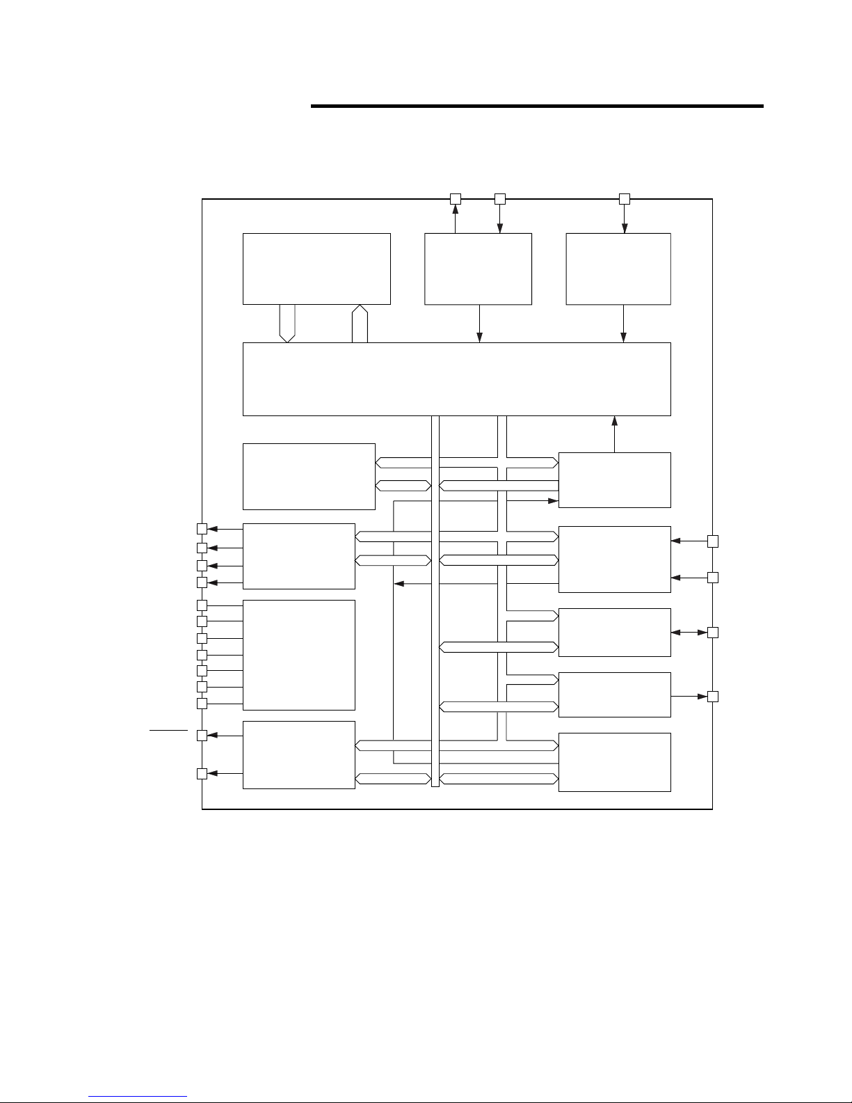
Each member of the E0C6001 Series of single chip microcomputers feature a 4-bit E0C6200B core CPU, 1,024 words
of ROM (12 bits per word), 80 words of RAM (4 bits per
word), an LCD driver, 4 bits for input ports (K00–K03), 2
bits for output ports (R00, R01), one 4-bit I/O port (P00–
P03) and one timer (clock timer).
Because of their low voltage operation and low power consumption, the E0C6001 Series are ideal for a wide range of
applications.
Configuration
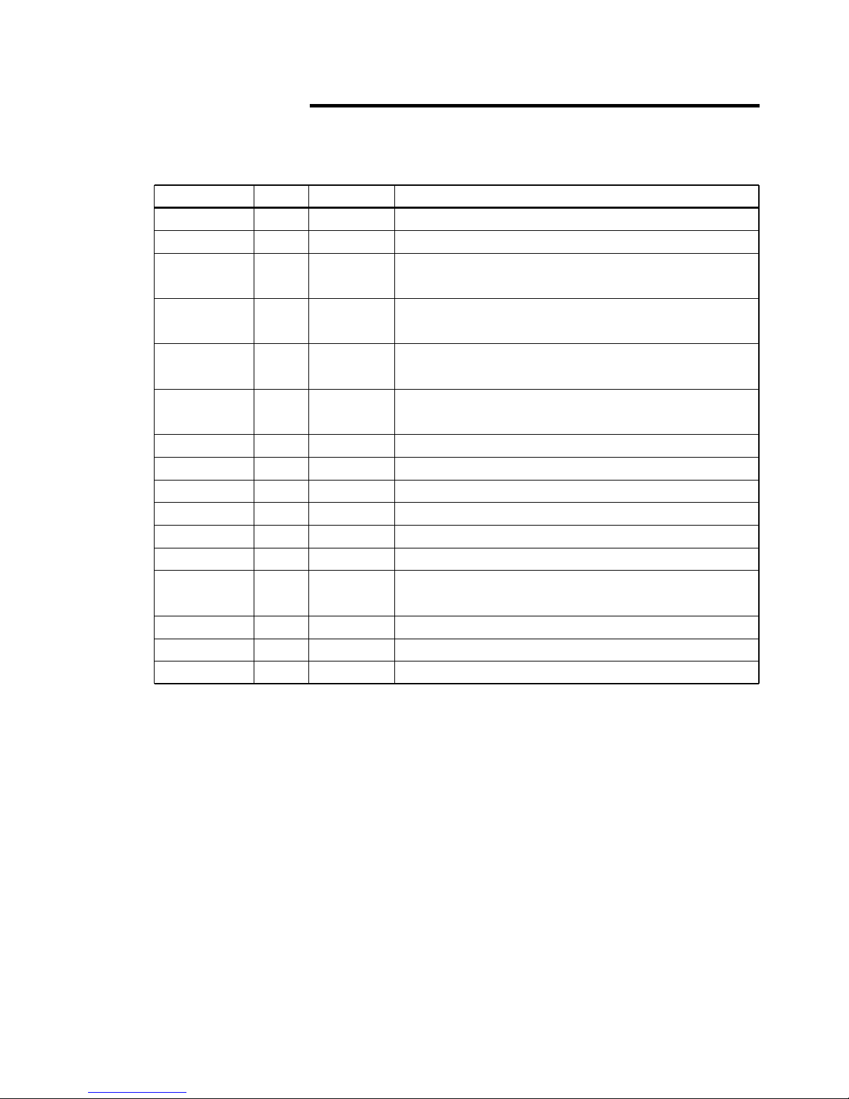
The E0C6001 Series are configured as follows, depending on
the supply voltage.
CHAPTER 1
1.1
Table 1.1.1
Configuration of the
E0C6001 Series
Model Supply Voltage Oscillation Circuits
3.0 V
1.5 V
E0C6001
E0C60L01
Crystal or CR
Crystal or CR
Supply Voltage Range
1.8–3.6 V
1.2–2.0 V
Page 9

E0C6001 TECHNICAL HARDWARE
I-2
Features
Crystal or CR oscillation circuit, 32.768 kHz (typ.)
100 instructions
1,024 words ×12 bits
80 words × 4 bits
4 bits (Supplementary pull-down resistors may be used )
2 bits (Piezo buzzer and programmable frequency output
can be driven directry by mask option)
4 bits
20 segments × 4, 3 or 2 common duty
1 system: clock timer
Input port interrupt 1 system
Timer interrupt 1 system
1.5 V (1.2–2.0 V) E0C60L01
3.0 V (1.8–3.6 V) E0C6001
1.0 µA
(Crystal oscillation CLK = 32.768 kHz, when halted)
2.5 µA
(Crystal oscillation CLK = 32.768 kHz, when executing)
QFP12-48pin (plastic) or chip
1.2
Built-in oscillation circuit
Instruction set
ROM capacity
RAM capacity (data RAM)
Input port
Output port
Input/output port
LCD driver
Timer
Interrupts:
External interrupt
Internal interrupt
Supply voltage
Current consumption (typ.)
Supply form
Page 10
CHAPTER 1: INTRODUCTION
I-3
1.3
Fig. 1.3.1
Block diagram
Power
Controller
LCD
Driver
RAM
80
× 4
Interrupt
Generator
I Port
Test Port
I/O Port
O Port
Timer
Core CPU E0C6200B
ROM
1,024 × 12
OSC
System
Reset
Control
RESET
OSC1
COM0
|
COM3
SEG0
|
SEG19
VDD
VL1
|
VL3
CA
CB
VS1
VSS
K00~K03
TEST
P00~P03
R00, R01
OSC2
FOUT
&
BUZZER
(FOUT/BUZZER)
(BUZZER)
Block Diagram
Page 11
E0C6001 TECHNICAL HARDWARE
I-4
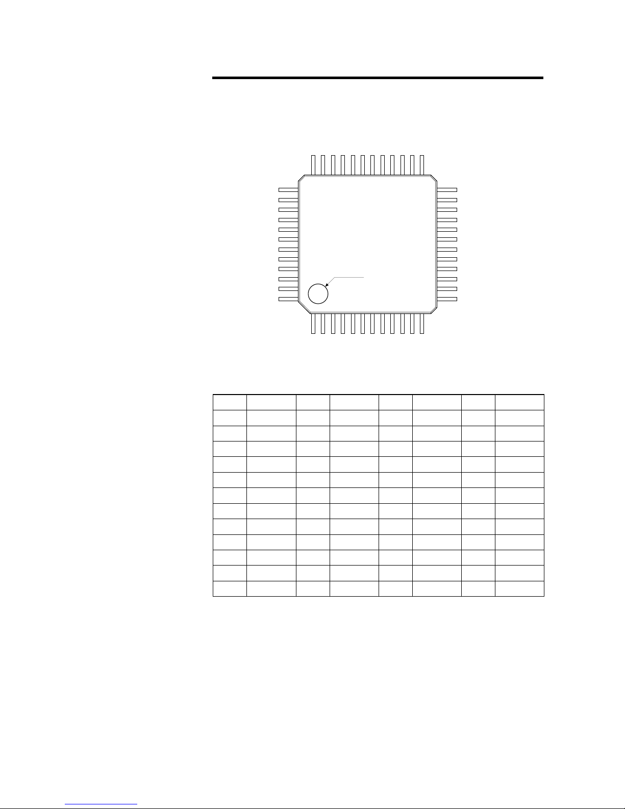
1.4
N.C. = No Connection
1
2
3
4
5
6
7
8
9
10
11
12
OSC2
V
S1
N.C.
P00
P01
P02
P03
K00
K01
K02
K03
N.C.
13
14
15
16
17
18
19
20
21
22
23
24
R01
R00
SEG19
SEG18
SEG17
SEG16
SEG15
SEG14
SEG13
SEG12
SEG11
SEG10
25
26
27
28
29
30
31
32
33
34
35
36
TEST
RESET
SEG9
SEG8
SEG7
SEG6
SEG5
SEG4
SEG3
SEG2
SEG1
SEG0
37
38
39
40
41
42
43
44
45
46
47
48
COM0
COM1
COM2
COM3
V
L3
VL2
VL1
CA
CB
V
SS
VDD
OSC1
Pin No Pin Name Pin No Pin Name Pin No Pin No Pin NamePin Name
Fig. 1.4.1
Pin assignment
QFP12-48pin
2536
13
24
INDEX
121
48
37
Pin Layout Diagram
Page 12
CHAPTER 1: INTRODUCTION
I-5
1.5
Table 1.5.1 Pin description
Terminal Name
V
DD
V
SS
V
S1
V
L1
V
L2
V
L3
CA, CB
OSC1
OSC2
K00–K03
P00–P03
R00, R01
SEG0–19
COM0–3
RESET
TEST
Pin No.
47
46
2
43
42
41
44, 45
48
1
8–11
4–7
14, 13
36–27
24–15
37–40
26
25
Input/Output
(I)
(I)
O
O
O
O
–
I
O
I
I/O
O
O
O
I
I
Function
Power source (+) terminal
Power source (-) terminal
Oscillation and internal logic system regulated
voltage output terminal
LCD system reducer output terminal (V
L2
× 1/2)
/ LCD system reducer output terminal (V
L3
× 1/3)
LCD system booster output terminal (V
L1
× 2)
/ LCD system reducer output terminal (V
L3
× 2/3)
LCD system booster output terminal (V
L1
× 3)
/ LCD system booster output terminal (V
L2
× 3/2)
Booster capacitor connecting terminal
Crystal or CR oscillation input terminal
Crystal or CR oscillation output terminal
Input terminal
I/O terminal
Output terminal
LCD segment output terminal
(convertible to DC output terminal by mask option)
LCD common output terminal
Initial setting input terminal
Test input terminal
Pin Description
Page 13

E0C6001 TECHNICAL HARDWARE
I-6
POWER SUPPLY AND INITIAL RESETCHAPTER 2
2.1
Power Supply
With a single external power supply (*1) supplied to VDD
through VSS, the E0C6001 Series generate the necessary
internal voltages with the regulated voltage circuit (<VS1> for
oscillators and internal circuit) and the voltage booster/
reducer (<VL2, VL3 or VL1, VL3> for LCDs).
When the E0C6001 LCD power is selected for 4.5 V LCD
panel by mask option, the E0C6001 short-circuits between
<VL2> and <VSS> in internally, and the voltage booster/
reducer generates <VL1> and <VL3>. When 3.0 V LCD panel
is selected, the E0C6001 short-circuits between <VL3> and
<VSS>, and the voltage reducer generates <VL1> and <VL2>.
The E0C60L01 short-circuits between <VL1> and <VSS>, and
the voltage booster generates <VL2> and <VL3>.
The voltage <VS1> for the internal circuit that is generated
by the regulated voltage circuit is -1.2 V (VDD standard).
Figure 2.1.1 shows the power supply configuration of the
E0C6001 Series in each condition.
*1 Supply voltage: E0C6001 ...... 3.0 V
E0C60L01 .... 1.5 V
- External loads cannot be driven by the output voltage of the
regulated voltage circuit and the voltage booster/reducer.
- See Chapter 6, "ELECTRICAL CHARACTERISTICS", for
voltage values.
Note
Page 14
CHAPTER 2: POWER SUPPLY AND INITIAL RESET
I-7
• E0C6001
4.5 V LCD panel
1/4, 1/3, 1/2 duty, 1/3 bias
Note: VL2 is shorted to VSS inside the IC.
3 V LCD panel 3 V LCD panel
1/4, 1/3, 1/2 duty, 1/3 bias 1/4, 1/3, 1/2 duty, 1/2 bias
• E0C60L01
4.5 V LCD panel 3 V LCD panel
1/4, 1/3, 1/2 duty, 1/3 bias 1/4, 1/3, 1/2 duty, 1/2 bias
Note: VL1 is shorted to VSS inside the IC.
Fig. 2.1.1 External element configuration of power system
Note: VL3 is shorted to VSS inside the IC.
V
DD
V
S1
V
L1
V
L2
V
L3
CA
CB
V
SS
3 V
V
DD
V
S1
V
L1
V
L2
V
L3
CA
CB
V
SS
3 V
V
DD
V
S1
V
L1
V
L2
V
L3
CA
CB
V
SS
3 V
V
DD
V
S1
V
L1
V
L2
V
L3
CA
CB
V
SS
1.5 V
V
DD
V
S1
V
L1
V
L2
V
L3
CA
CB
V
SS
1.5 V
Page 15
E0C6001 TECHNICAL HARDWARE
I-8
Initial Reset
To initialize the E0C6001 Series circuits, an initial reset
must be executed. There are three ways of doing this.
(1)Initial reset by the oscillation detection circuit (Note)
(2)External initial reset via the RESET pin
(3)External initial reset by simultaneous high input to pins
K00–K03 (depending on mask option)
Figure 2.2.1 shows the configuration of the initial reset
circuit.
Fig. 2.2.1
Configuration of
initial reset circuit
2.2
Vss
RESET
K03
K02
K01
K00
OSC2
OSC1
OSC1
Oscillation
circuit
Vss
Oscillation
detection
circuit
Noise
rejection
circuit
Initial
reset
Noise
rejection
circuit
Note Be sure to use reset function (2) or (3) at power-on because the
initial reset function by the oscillation detection circuit (1) may not
operate normally depending on the power-on procedure.
Page 16

CHAPTER 2: POWER SUPPLY AND INITIAL RESET
I-9
The oscillation detection circuit outputs the initial reset
signal at power-on until the crystal oscillation circuit starts
oscillating, or when the crystal oscillation circuit stops
oscillating for some reason.
However, use the following reset functions at power-on
because the initial reset function by the oscillation detection
circuit may not operate normally depending on the power-on
procedure.
An initial reset can be invoked externally by making the
reset pin high. This high level must be maintained for at
least 5 ms (when oscillating frequency, fosc = 32 kHz),
because the initial reset circuit contains a noise rejection
circuit. When the reset pin goes low the CPU begins to
operate.
Another way of invoking an initial reset externally is to input
a high signal simultaneously to the input ports (K00–K03)
selected with the mask option. The specified input port pins
must be kept high for at least 4 sec (when oscillating frequency fosc = 32 kHz), because of the noise rejection circuit.
Table 2.2.1 shows the combinations of input ports (K00–
K03) that can be selected with the mask option.
A Not used
B K00*K01
C K00*K01*K02
D K00*K01*K02*K03
When, for instance, mask option D (K00*K01*K02*K03) is
selected, an initial reset is executed when the signals input
to the four ports K00–K03 are all high at the same time.
If you use this function, make sure that the specified ports
do not go high at the same time during normal operation.
Oscillation detection
circuit
Reset pin (RESET)
Simultaneous high
input to input ports
(K00–K03)
Table 2.2.1
Input port combinations
Page 17
E0C6001 TECHNICAL HARDWARE
I-10
Internal register following initialization
Table 2.2.2
Initial values
2.3
An initial reset initializes the CPU as shown in the table
below.
CPU Core
Name
Program counter step
Program counter page
New page pointer
Stack pointer
Index register X
Index register Y
Register pointer
General register A
General register B
Interrupt flag
Decimal flag
Zero flag
Carry flag
Signal
PCS
PCP
NPP
SP
X
Y
RP
A
B
I
D
Z
C
Number of Bits
8
4
4
8
8
8
4
4
4
1
1
1
1
Setting Value
00H
1H
1H
Undefined
Undefined
Undefined
Undefined
Undefined
Undefined
0
0
Undefined
Undefined
Peripheral Circuits
Name
RAM
Display memory
Other peripheral circuit
Number of Bits
80 × 4
20 × 4
–
Setting Value
Undefined
Undefined
*1
*1: See section 4.1, "Memory Map"
Test Pin (TEST)
This pin is used when IC is inspected for shipment.
During normal operation connect it to VSS.
Page 18

I-11
CHAPTER 3: CPU, ROM, RAM
CPU, ROM, RAM
CPU
The E0C6001 Series employs the E0C6200B core CPU, so
that register configuration, instructions, and so forth are
virtually identical to those in other processors in the family
using the E0C6200B. Refer to the "E0C6200/6200A Core
CPU Manual" for details of the E0C6200B.
Note the following points with regard to the E0C6001 Series:
(1)The SLEEP operation is not provided, so the SLP instruc-
tion cannot be used.
(2)Because the ROM capacity is 1,024 words, 12 bits per
word, bank bits are unnecessary, and PCB and NBP are
not used.
(3)The RAM page is set to 0 only, so the page part (XP, YP)
of the index register that specifies addresses is invalid.
PUSH XP PUSH YP
POP XP POP YP
LD XP,r LD YP,r
LD r,XP LD r,YP
CHAPTER 3
3.1
Page 19
E0C6001 TECHNICAL HARDWARE
I-12
3.2 ROM
The built-in ROM, a mask ROM for the program, has a
capacity of 1,024 × 12-bit steps. The program area is 4
pages (0–3), each consisting of 256 steps (00H–FFH). After
an initial reset, the program start address is page 1, step
00H. The interrupt vector is allocated to page l, steps 01H–
07H.
3.3
Fig. 3.2.1
ROM configuration
RAM
The RAM, a data memory for storing a variety of data, has a
capacity of 80 words, 4-bit words. When programming,
keep the following points in mind:
(1)Part of the data memory is used as stack area when
saving subroutine return addresses and registers, so be
careful not to overlap the data area and stack area.
(2)Subroutine calls and interrupts take up three words on
the stack.
(3)Data memory 000H–00FH is the memory area pointed by
the register pointer (RP).
00H step
07H step
08H step
FFH step
12 bits
Program start address
Interrupt vector area
Bank 0
Program area
0 page
1 page
2 page
3 page
01H step
Page 20
CHAPTER 4: PERIPHERAL CIRCUITS AND OPERATION (Memory Map)
I-13
PERIPHERAL CIRCUITS
AND OPERATION
Peripheral circuits (timer, I/O, and so on) of the E0C6001
Series are memory mapped. Thus, all the peripheral circuits
can be controlled by using memory operations to access the
I/O memory. The following sections describe how the peripheral circuits operate.
CHAPTER 4
Memory Map
The data memory of the E0C6001 Series has an address
space of 113 words, of which 32 words are allocated to
display memory and 13 words, to I/O memory. Figure 4.1.1
show the overall memory map for the E0C6001 Series, and
Tables 4.1.1(a)–(d), the memory maps for the peripheral
circuits (I/O space).
4.1
Unused area
Fig. 4.1.1
Memory map
Note Memory is not mounted in unused area within the memory map
and in memory area not indicated in this chapter. For this reason,
normal operation cannot be assured for programs that have been
prepared with access to these areas.
Address
Page High
Low
0123456789ABCDE
F
M0 M1 M2 M3 M4 M5 M6 M7 M8 M9 MA MB MC MD ME MF
3
0
1
2
4
5
6
7
8
9
A
B
C
D
E
F
0
RAM area (000H–04FH)
80 words x 4 bits (R/W)
Display memory area (090H–0AFH)
32 words x 4 bits (Write only)
I/O memory area Tables 4.1.1(a)–(d)
Page 21
E0C6001 TECHNICAL HARDWARE
I-14
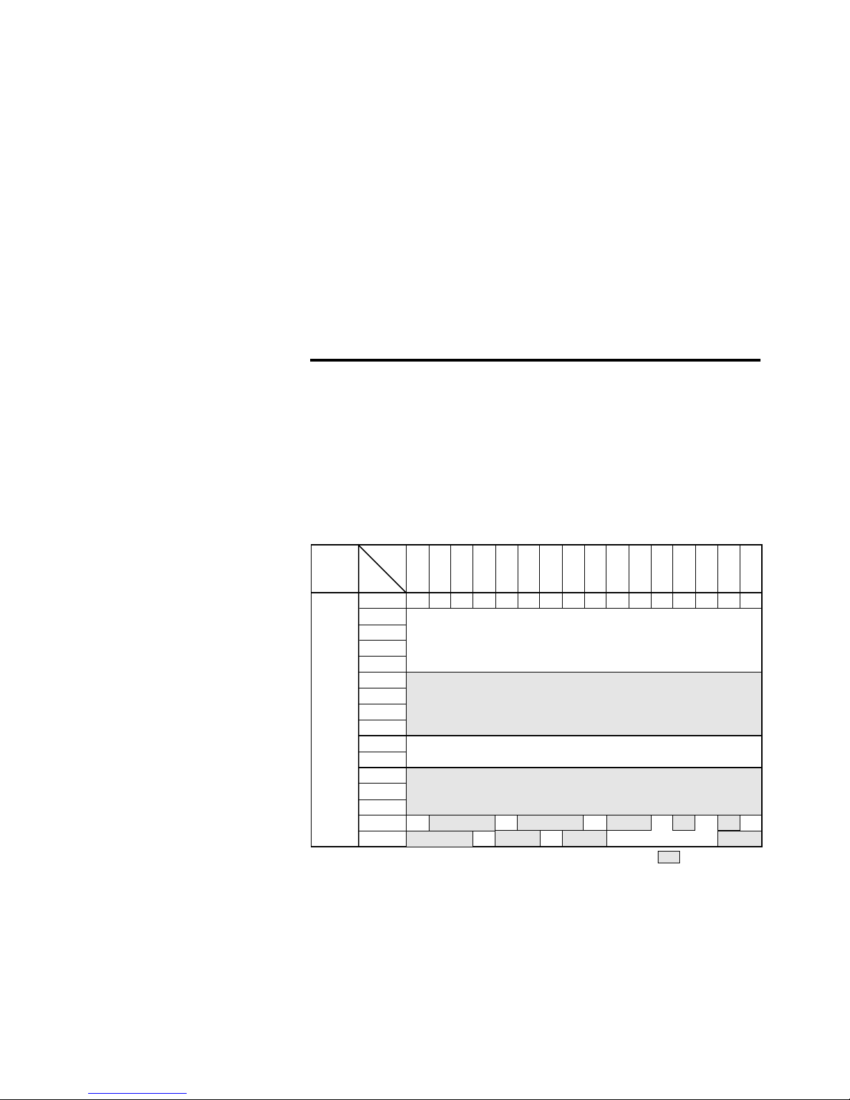
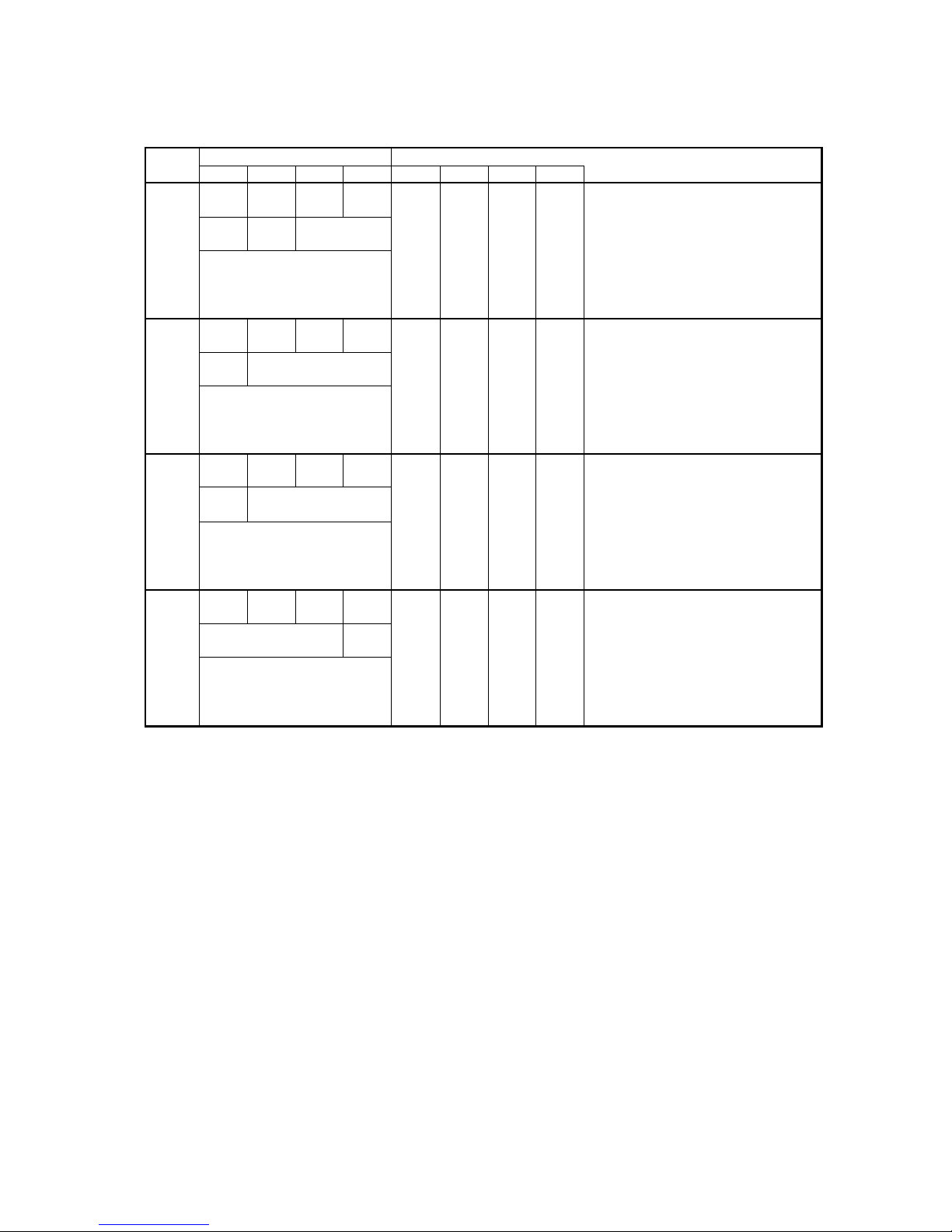
Table 4.1.1(a) I/O memory map
* 1 Initial value following initial reset
* 2 Not set in the circuit
* 3 Undefined
* 4 Reset (0) immediately after being read
* 5 Constantly 0 when being read
* 6 Refer to main manual
Address Comment
Register
D3 D2 D1 D0 Name SR
*1
10
0E0H
0E4H
0E8H
K03 K02 K01 K00
TM3 TM2 TM1 TM0
EIK03 EIK02 EIK01 EIK00
R/W
R
R
K03
K02
K01
K00
–
–
–
–
TM3
TM2
TM1
TM0
–
–
–
–
EIK03
EIK02
EIK01
EIK00
0
0
0
0
Enable
Enable
Enable
Enable
Mask
Mask
Mask
Mask
Timer data (clock timer 2 Hz)
Timer data (clock timer 4 Hz)
Timer data (clock timer 8 Hz)
Timer data (clock timer 16 Hz)
Input port (K00–K03)
High
High
High
High
Low
Low
Low
Low
Interrupt mask register (K03)
Interrupt mask register (K02)
Interrupt mask register (K01)
Interrupt mask register (K00)
High
High
High
High
Low
Low
Low
Low
*2
*2
*2
*2
0 EIT2 EIT8 EIT32 0
EIT2
EIT8
EIT32
0
0
0
Interrupt mask register (clock timer 2 Hz)
Interrupt mask register (clock timer 8 Hz)
Interrupt mask register (clock timer 32 Hz)
Enable
Enable
Enable
Mask
Mask
Mask
0EBH
R R/W
*5
Page 22
CHAPTER 4: PERIPHERAL CIRCUITS AND OPERATION (Memory Map)
I-15
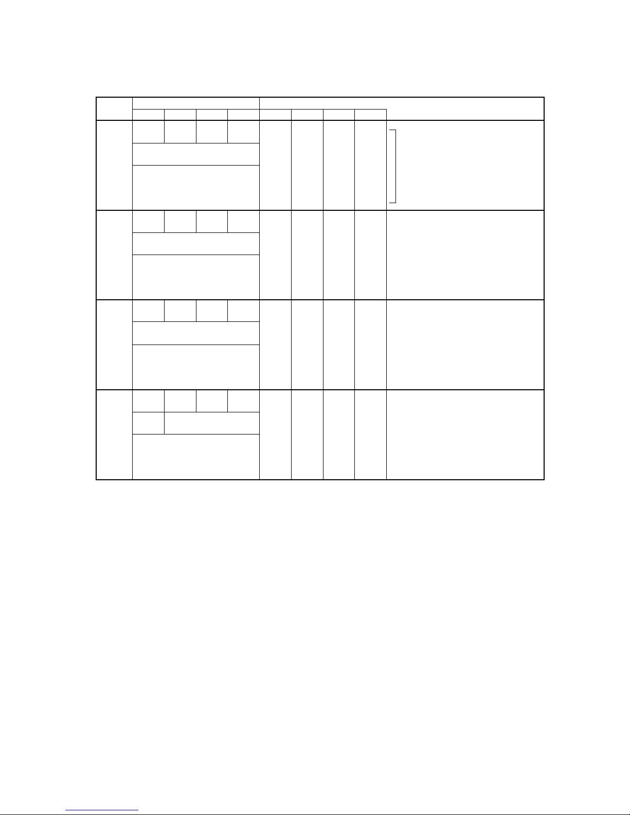
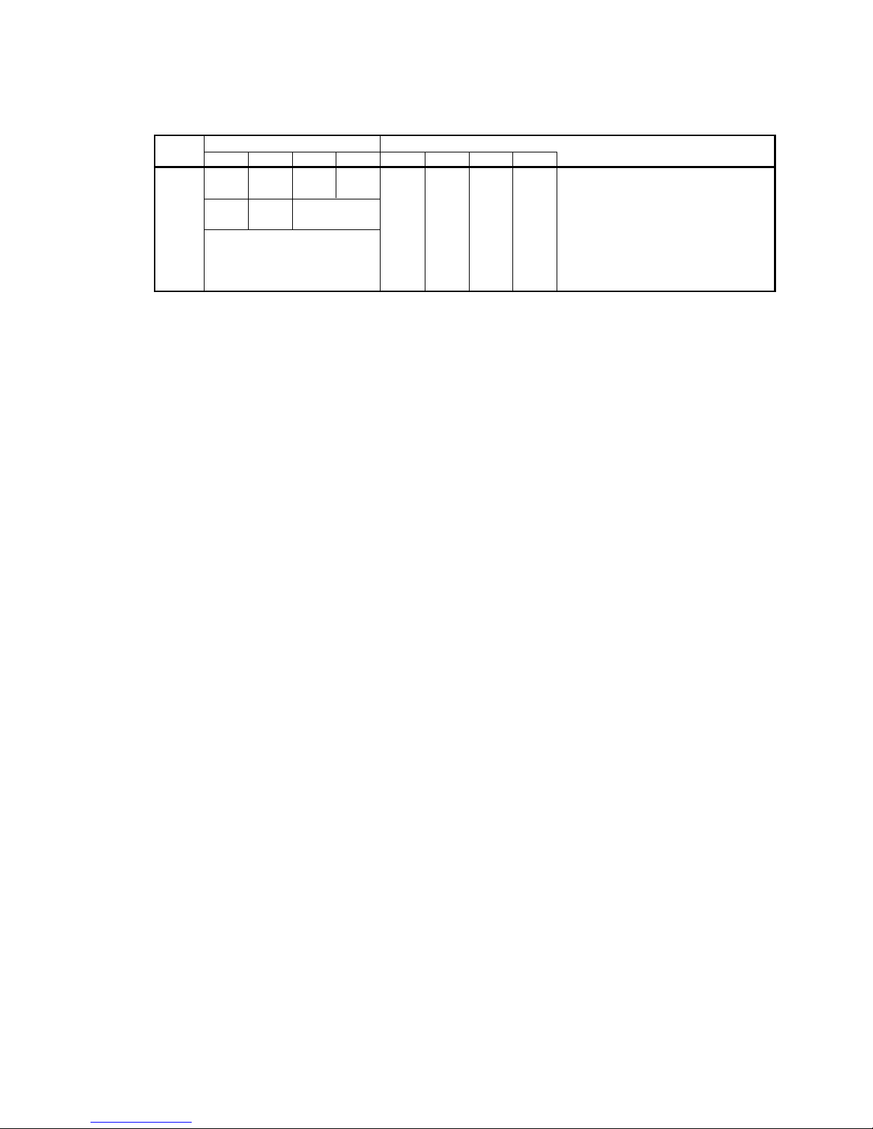
Table 4.1.1(b) I/O memory map
* 1 Initial value following initial reset
* 2 Not set in the circuit
* 3 Undefined
* 4 Reset (0) immediately after being read
* 5 Constantly 0 when being read
* 6 Refer to main manual
Address Comment
Register
D3 D2 D1 D0 Name SR
*1
10
0EDH
0EFH
0 0 0 IK0
0 IT2 IT8 IT32
0
0
0
IK0
0
0
IT2
IT8
IT32
0
0
0
Yes
Yes
Yes
Interrupt factor flag (K00–K03)
Interrupt factor flag (clock timer 2 Hz)
Interrupt factor flag (clock timer 8 Hz)
Interrupt factor flag (clock timer 32 Hz)
Yes No
R
R
*5
*5
*5
*4
0F6H
P03 P02 P01 P00
P03
P02
P01
P00
–
–
–
–
I/O port (P00–P03)
High
High
High
High
Low
Low
Low
Low
*2
*2
*2
*2
R/W
*5
*4
*4
*4
*5
*5
No
No
No
0F3H
00
R01 R00
0
0
R01
BUZZER
R00
FOUT
0
0
0
0
High
ON
High
ON
Low
OFF
Low
OFF
R01 output port data
Buzzer ON/OFF control register
R00 output port data
Frequency output ON/OFF control register
R/WR
BUZZER FOUT
Page 23
E0C6001 TECHNICAL HARDWARE
I-16
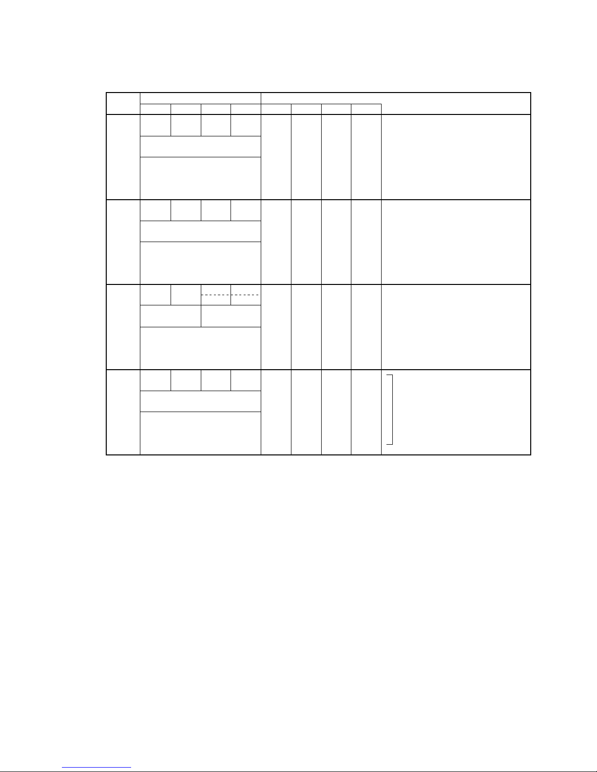
Table 4.1.1(c) I/O memory map
* 1 Initial value following initial reset
* 2 Not set in the circuit
* 3 Undefined
* 4 Reset (0) immediately after being read
* 5 Constantly 0 when being read
* 6 Refer to main manual
Address Comment
Register
D3 D2 D1 D0 Name SR
*1
10
0F9H
0FAH
0 TMRST 0 0
HLMOD 0 0 0
W
0
TMRST
0
0
Reset
HLMOD
0
0
0
0
Clock timer reset
Heavy load protection mode register
Reset –
R
RR
R/W
Heavy
load
Normal
load
*5
*5
*5
0FBH
0FCH
CSDC 0 0 0
0 0 0 IOC
R
R
0
0
0
0
IOC
0
I/O port P00–P03 Input/Output
LCD drive switch
Static Dynamic
Output Input
*5
*5
*5
*5
*5
*5
R/W
R/W
CSDC
0
0
0
*5
*5
*5
Page 24
CHAPTER 4: PERIPHERAL CIRCUITS AND OPERATION (Memory Map)
I-17
Table 4.1.1(d) I/O memory map
* 1 Initial value following initial reset
* 2 Not set in the circuit
* 3 Undefined
* 4 Reset (0) immediately after being read
* 5 Constantly 0 when being read
* 6 Refer to main manual
Address Comment
Register
D3 D2 D1 D0 Name SR
*1
10
0FDH
XBZR 0 XFOUT1 XFOUT0RXBZR
0
XFOUT1
XFOUT0
0
0
0
Buzzer frequency control
2 kHz
High
High
4 kHz
Low
Low
R/WR/W
*5
FOUT frequency control:
XFOUT1(0), XFOUT0(0) -> F1
XFOUT1(0), XFOUT0(1) -> F2
XFOUT1(1), XFOUT0(0) -> F3
XFOUT1(1), XFOUT0(1) -> F4
Page 25
E0C6001 TECHNICAL HARDWARE
I-18
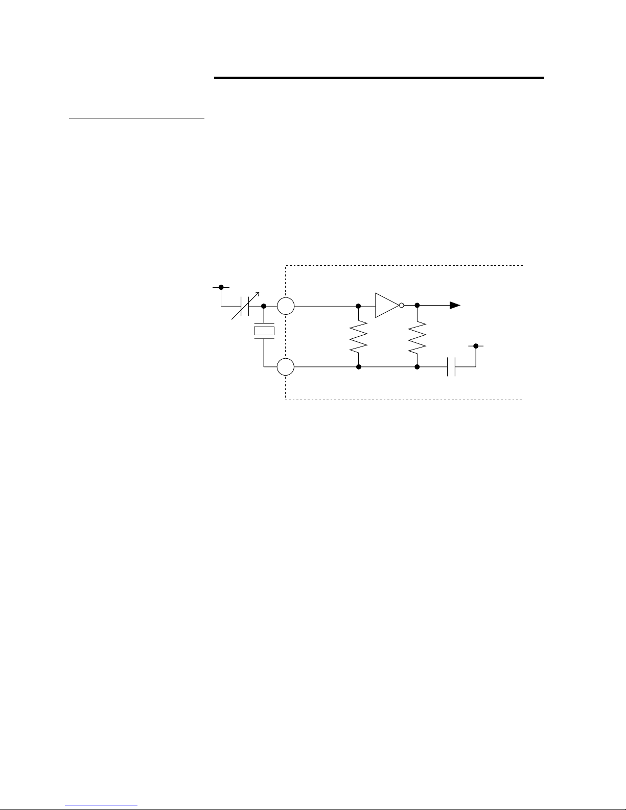
Oscillation Circuit
The E0C6001 Series have a built-in crystal oscillation
circuit. This circuit generates the operating clock for the
CPU and peripheral circuit on connection to an external
crystal oscillator (typ. 32.768 kHz) and trimmer capacitor
(5–25 pF).
Figure 4.2.1 is the block diagram of the crystal oscillation
circuit.
4.2
Fig. 4.2.1
Crystal oscillation circuit
Crystal oscillation
circuit
As Figure 4.2.1 indicates, the crystal oscillation circuit can
be configured simply by connecting the crystal oscillator
(X'tal) between the OSC1 and OSC2 pins and the trimmer
capacitor (CG) between the OSC1 and VDD pins.
C
G
X'tal
OSC2
OSC1
To CPU and
peripheral circuits
The E0C6001 Series
V
DD
Rf
R
D
C
D
V
DD
Note
The OSC1 and OSC2 terminals on the board should be shielded
with the VDD (+ side)
.
Page 26
CHAPTER 4: PERIPHERAL CIRCUITS AND OPERATION (Oscillation Circuit)
I-19
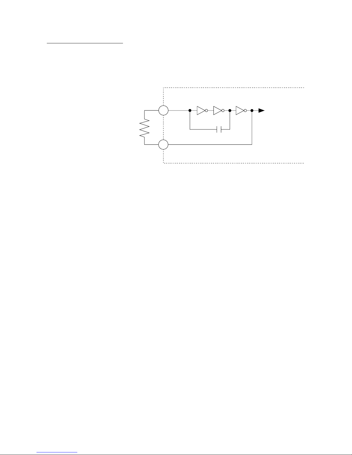
CR oscillation circuit
For the E0C6001 Series, CR oscillation circuit (typ. 65 kHz)
may also be selected by a mask option. Figure 4.2.2 is the
block diagram of the CR oscillation circuit.
Fig. 4.2.2
CR oscillation circuit
As Figure 4.2.2 indicates, the CR oscillation circuit can be
configured simply by connecting the register (R) between
pins OSC1 and OSC2 since capacity (C) is built-in.
See Chapter 6, "ELECTRICAL CHARACTERISTICS" for R
value.
OSC2
OSC1
C
To CPU and
peripheral circuits
The E0C6001 Series
R
Page 27
E0C6001 TECHNICAL HARDWARE
I-20
Input Port (K00–K03)
The E0C6001 Series have a 4-bit general-purpose input
port. Each of the input port pins (K00–K03) has an internal
pull-down resistance. The pull-down resistance can be
selected for each bit with the mask option.
Figure 4.3.1 shows the configuration of input port.
Selecting "pull-down resistance enabled" with the mask
option allows input from a push button, key matrix, and so
forth. When "pull-down resistance disabled" is selected, the
port can be used for slide switch input and interfacing with
other LSIs.
4.3
Configuration of
input port
Fig. 4.3.1
Configuration of input port
All four input port bits (K00–K03) provide the interrupt
function. The conditions for issuing an interrupt can be set
by the software for the four bits. Also, whether to mask the
interrupt function can be selected individually for all four
bits by the software. Figure 4.3.2 shows the configuration of
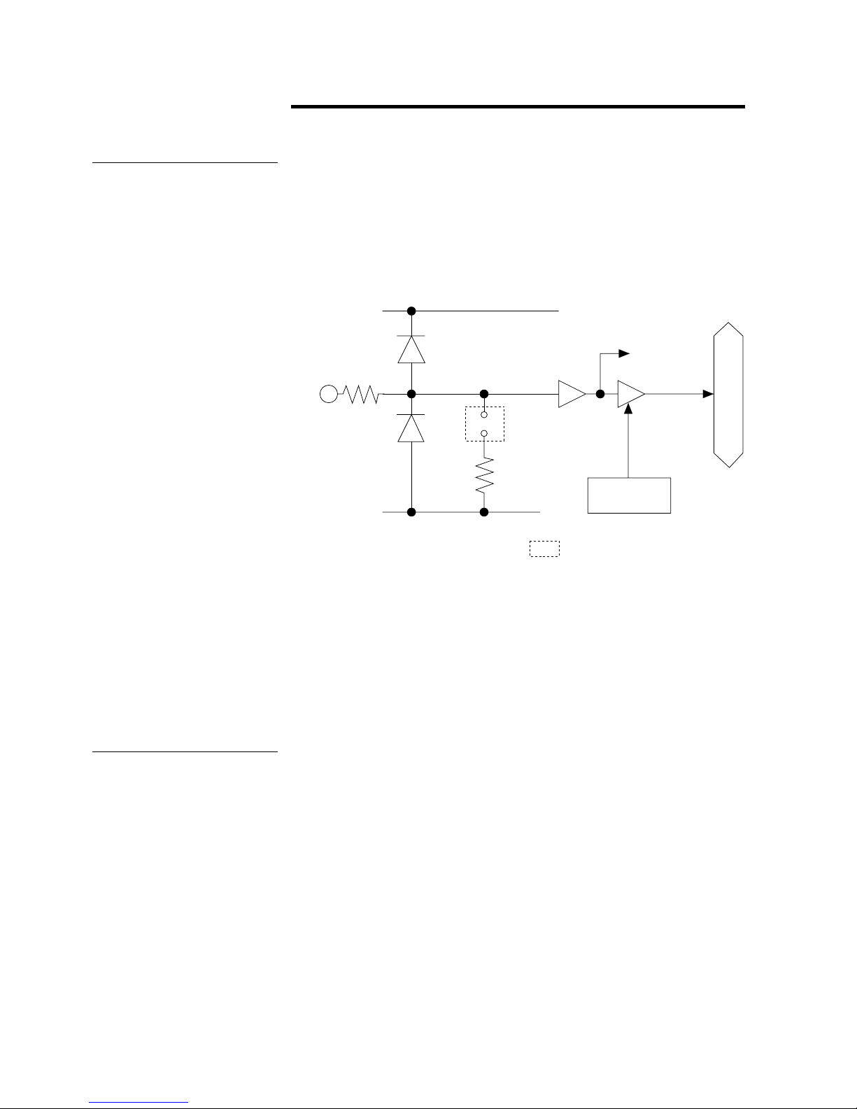
K00–K03.
Interrupt function
Kxx
V
SS
Mask option
Address
V
DD
Interrupt
request
Data bus
Page 28
CHAPTER 4: PERIPHERAL CIRCUITS AND OPERATION (Input Port)
I-21
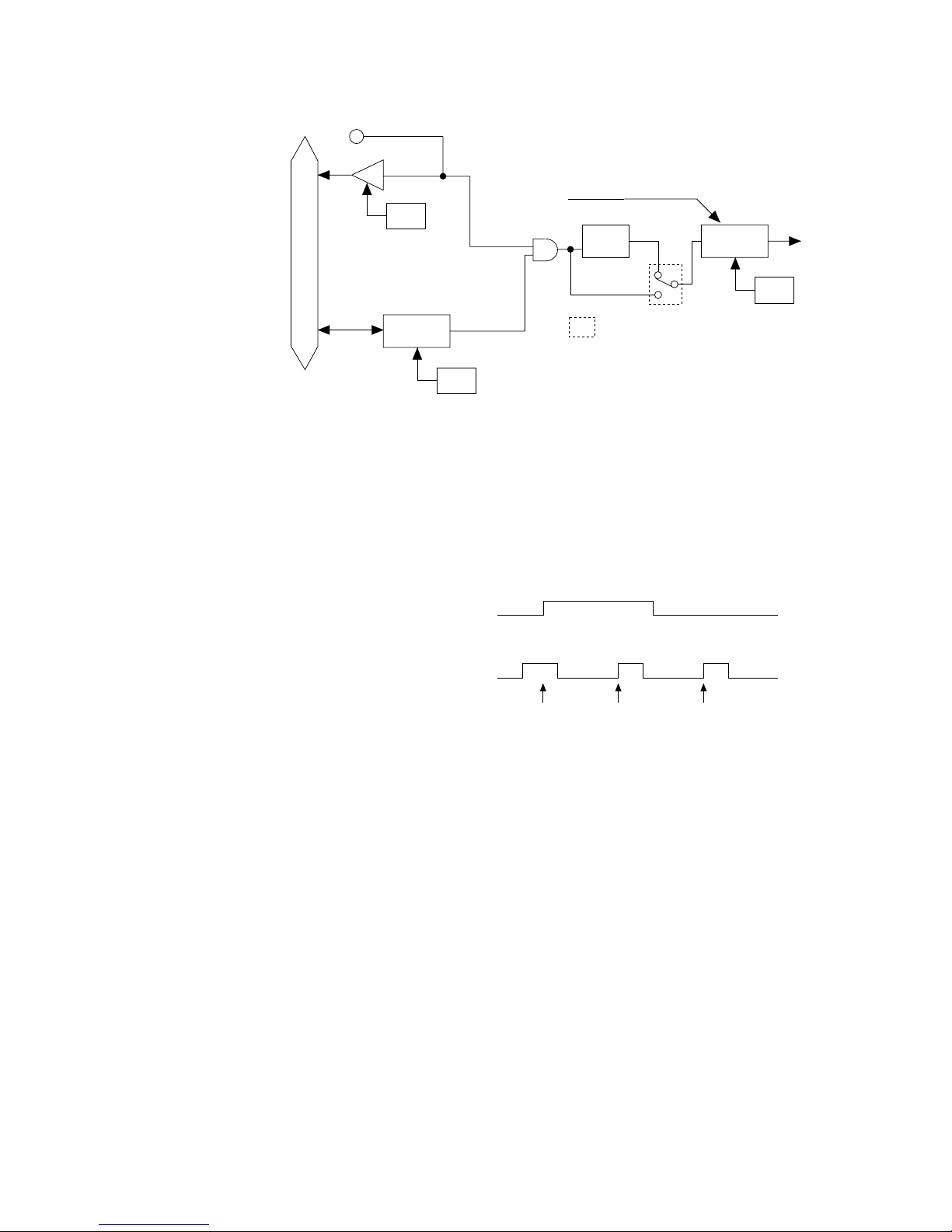
Fig. 4.3.3
Input interrupt timing
Input interrupt programing related precautions
When the content of the mask register is rewritten, while
the port K input is in the active status. The input interrupt
factor flag is set at ➀.
The interrupt mask registers (EIK00–EIK03) enable the
interrupt mask to be selected individually for K00–K03. An
interrupt occurs when the input value which are not
masked change and the interrupt factor flag (IK0) is set to 1.
Fig. 4.3.2
Input interrupt circuit
configuration
(K00–K03)
When using an input interrupt, if you rewrite the content of
the mask register, when the value of the input terminal
which becomes the interrupt input is in the active status
(input terminal = high status), the factor flag for input
interrupt may be set.
For example, a factor flag is set with the timing of ➀ shown
in Figure 4.3.3. However, when clearing the content of the
mask register with the input terminal kept in the high
status and then setting it, the factor flag of the input interrupt is again set at the timing that has been set.
Data bus
Address
Interrupt mask
register (EIK)
Kxx
Mask option
(K00–K03)
Noise
rejector
One for each pin series
Interrupt factor
flag (IK)
Interrupt
request
Address
Address
Port K input
Factor flag set Not set
Mask register
Active status
➀
Page 29

E0C6001 TECHNICAL HARDWARE
I-22
Consequently, when the input terminal is in the active
status (high status), do not rewrite the mask register (clearing, then setting the mask register), so that a factor flag will
only set at the rising edge in this case. When clearing, then
setting the mask register, set the mask register, when the
input terminal is not in the active status (low status).
The contents that can be selected with the input port mask
option are as follows:
(1) An internal pull-down resistance can be selected for each
of the four bits of the input ports (K00–K03). Having
selected "pull-down resistance disabled", take care that
the input does not float. Select "pull-down resistance
enabled" for input ports that are not being used.
(2) The input interrupt circuit contains a noise rejection
circuit to prevent interrupts form occurring through
noise. The mask option enables selection of the noise
rejection circuit for each separate pin series. When "use"
is selected, a maximum delay of 0.5 ms (fosc = 32 kHz)
occurs from the time an interrupt condition is established
until the interrupt factor flag (IK) is set to 1.
Mask option
Page 30
CHAPTER 4: PERIPHERAL CIRCUITS AND OPERATION (Input Port)
I-23
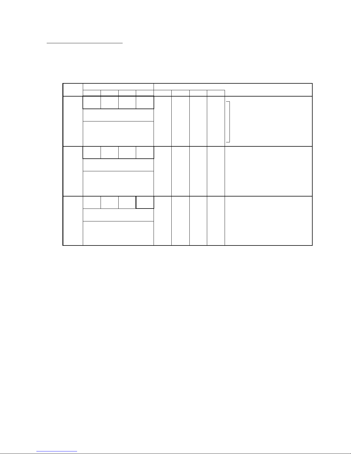
Table 4.3.1 list the input port control bits and their addresses.
Table 4.3.1 Input port control bits
Control of input port
Address Comment
Register
D3 D2 D1 D0 Name SR 1 0
0E0H
K03 K02 K01 K00
R
K03
K02
K01
K00
–
–
–
–
Input port (K00–K03)
High
High
High
High
Low
Low
Low
Low
0E8H
EIK03 EIK02 EIK01 EIK00
R/W
EIK03
EIK02
EIK01
EIK00
0
0
0
0
Interrupt mask register (K03)
Interrupt mask register (K02)
Interrupt mask register (K01)
Interrupt mask register (K00)
Enable
Enable
Enable
Enable
Mask
Mask
Mask
Mask
0EDH
0 0 IK0
R
0
0
0
IK0
0
Interrupt factor flag (K00–K03)
Yes No
0
K00–K03 Input port data (0E0H)
The input data of the input port pins can be read with these
registers.
When 1 is read: High level
When 0 is read: Low level
Writing: Invalid
The value read is 1 when the pin voltage of the four bits of
the input port (K00–K03) goes high (VDD), and 0 when the
voltage goes low (VSS). These bits are reading, so writing
cannot be done.
Page 31

E0C6001 TECHNICAL HARDWARE
I-24
Interrupt mask registers (0E8H)
Masking the interrupt of the input port pins can be done
with these registers.
When 1 is written: Enable
When 0 is written: Mask
Reading: Valid
With these registers, masking of the input port bits can be
done for each of the four bits. After an initial reset, these
registers are all set to 0.
EIK00–EIK03
IK0 Interrupt factor flag (0EDH)
This flag indicates the occurrence of an input interrupt.
When 1 is read: Interrupt has occurred
When 0 is read: Interrupt has not occurred
Writing: Invalid
The interrupt factor flag IK0 is associated with K00–K03.
From the status of this flag, the software can decide whether
an input interrupt has occurred.
This flag is reset when the software has read it.
Reading of interrupt factor flag is available at EI, but be
careful in the following cases.
If the interrupt mask register value corresponding to the
interrupt factor flag to be read is set to 1, an interrupt
request will be generated by the interrupt factor flag set
timing, or an interrupt request will not be generated.
After an initial reset, this flag is set to 0.
Page 32

CHAPTER 4: PERIPHERAL CIRCUITS AND OPERATION (Output Port)
I-25
Output Port (R00, R01)
The E0C6001 Series have a 2-bit general output port (R00,
R01).
Output specification of the output port can be selected in a
bit unit with the mask option. Two kinds of output specifications are available: complementary output and Pch open
drain output. Also, the mask option enables the output
ports R00 and R01 to be used as special output ports.
Figure 4.4.1 shows the configuration of the output port.
Configuration of
output port
4.4
Fig. 4.4.1
Configuration of output port
Register
Data bus
Address
V
DD
V
SS
Rxx
Complementary
Pch open drain
Mask option
Page 33

E0C6001 TECHNICAL HARDWARE
I-26
The mask option enables the following output port selection.
(1)Output specification of output port
The output specifications for the output port (R00, R01)
may be either complementary output or Pch open drain
output for each of the two bits. However, even when Pch
open drain output is selected, a voltage exceeding the
source voltage must not be applied to the output port.
(2)Special output
In addition to the regular DC output, special output can
be selected for output ports R00 and R01, as shown in
Table 4.4.1. Figure 4.4.2 shows the structure of output
ports R00 and R01.
Mask option
Table 4.4.1
Special output
FOUT or BUZZER
BUZZER
R00
R01
Pin Name When Special Output is Selected
Fig. 4.4.2
Structure of output ports
R00, R01
Address
(0F3H)
Data bus
Mask option
R01
R00
Register
(R01)
Register
(R00)
FOUT
BUZZER
BUZZER
Page 34

CHAPTER 4: PERIPHERAL CIRCUITS AND OPERATION (Output Port)
I-27
FOUT (R00) When output port R00 is set for FOUT output, this port will
generate fosc (CPU operating clock frequency) or clock
frequency divided into fosc. Clock frequency may be selected individually for F1–F4, from among 5 types by mask
option; one among F1–F4 is selected by software and used.
The types of frequency which may be selected are shown in
Table 4.4.2.
Output ports R01 and R00 may be set to BUZZER output
and BUZZER output (BUZZER reverse output), respectively,
allowing for direct driving of the piezo-electric buzzer.
BUZZER output (R00) may only be set if R01 is set to
BUZZER output. In such case, whether ON/OFF of the
BUZZER output is done through R00 register or is controlled through R01 simultaneously with BUZZER output is
also selected by mask option.
The frequency of buzzer output may be selected by software
to be either 2 kHz or 4 kHz.
Table 4.4.2
FOUT clock frequency
A hazard may occur when the FOUT signal is turned on or off.Note
(D1, D0) = (XFOUT1, XFOUT0)
Mask
Option
Sets
Clock Frequency (Hz)
Set 4
256
(fosc/128)
512
(fosc/64)
1,024
(fosc/32)
2,048
(fosc/16)
512
(fosc/64)
1,024
(fosc/32)
2,048
(fosc/16)
8,192
(fosc/4)
1,024
(fosc/32)
2,048
(fosc/16)
4,096
(fosc/8)
4,096
(fosc/8)
8,192
(fosc/4)
16,384
(fosc/2)
4,096
(fosc/8)
32,768
(fosc/1)
2,048
(fosc/16)
4,096
(fosc/8)
8,192
(fosc/4)
16,384
(fosc/2)
Set 1
Set 2
Set 3
Set 5
(D1,D0)=(0,0) (D1,D0)=(0,1) (D1,D0)=(1,0) (D1,D0)=(1,1)
F1 F2 F3 F4
fosc = 32.768 kHz
BUZZER, BUZZER
(R01, R00)
Page 35

E0C6001 TECHNICAL HARDWARE
I-28
Output port data (0F3H D0, 0F3H D1)
Sets the output data for the output ports.
When 1 is written: High output
When 0 is written: Low output
Reading: Valid
The output port pins output the data written to the corresponding registers (R00, R01) without changing it. When 1
is written to the register, the output port pin goes high
(VDD), and when 0 is written, the output port pin goes low
(VSS). After an initial reset, all the registers are set to 0.
R00, R01
Table 4.4.3 lists the output port control bits and their addresses.
Table 4.4.3 Control bits of output port
Control of output
port
Address Comment
Register
D3 D2 D1 D0 Name SR 1 0
0F3H
00
R01 R00
0
0
R01
BUZZER
R00
FOUT
0
0
0
0
High
ON
High
ON
Low
OFF
Low
OFF
R01 output port data
Buzzer ON/OFF control register
R00 output port data
Frequency output ON/OFF control register
R/WR
BUZZER FOUT
0FDH
XBZR 0 XFOUT1 XFOUT0RXBZR
0
XFOUT1
XFOUT0
0
0
0
Buzzer frequency control
2 kHz
High
High
4 kHz
Low
Low
R/WR/W
FOUT frequency control:
XFOUT1(0), XFOUT0(0) -> F1
XFOUT1(0), XFOUT0(1) -> F2
XFOUT1(1), XFOUT0(0) -> F3
XFOUT1(1), XFOUT0(1) -> F4
Page 36

CHAPTER 4: PERIPHERAL CIRCUITS AND OPERATION (Output Port)
I-29
Special output port data (0F3H D0)
Controls the FOUT (clock) output.
When 1 is written: Clock output
When 0 is written: Low level (DC) output
Reading: Valid
FOUT output can be controlled by writing data to R00. After
an initial reset, this register is set to 0.
Figure 4.4.3 shows the output waveform for FOUT output.
R00 (when FOUT is
selected)
Fig. 4.4.3
FOUT output waveform
FOUT frequency control (0FDH D0, 0FDH D1)
Selects the output frequency when R00 port is set for FOUT
output.
XFOUT0, XFOUT1
Table 4.4.4
FOUT frequency selection
After an initial reset, these registers are set to 0.
0
0
1
1
XFOUT1
0
1
0
1
XFOUT0
F1
F2
F3
F4
Frequency Selection
R00 register
FOUT output
waveform
01
Page 37

E0C6001 TECHNICAL HARDWARE
I-30
Special output port data (0F3H D0, 0F3H D1)
Controls the buzzer output.
When 1 is written: Buzzer output
When 0 is written: Low level (DC) output
Reading: Valid
BUZZER and BUZZER output can be controlled by writing
data to R00 and R01.
When BUZZER output by R01 register control is selected by
mask option, BUZZER output and BUZZER output can be
controlled simultaneously by writing data to R01 register.
After an initial reset, these registers are set to 0.
Figure 4.4.4 shows the output waveform for buzzer output.
R00, R01 (when BUZZER
and BUZZER is
selected)
Fig. 4.4.4
Buzzer output waveform
Buzzer frequency control (0FDH D3)
Selects the frequency of the buzzer signal.
When 1 is written: 2 kHz
When 0 is written: 4 kHz
Reading: Valid
When R00 and R01 port is set to buzzer output, the frequency of the buzzer signal can be selected by this register.
When 1 is written to this register, the frequency is set in 2
kHz, and in 4 kHz when 0 is written.
After an initial reset, this register is set to 0.
XBZR
R01 (R00) register
BUZZER output
waveform
01
BUZZER output
waveform
Page 38

CHAPTER 4: PERIPHERAL CIRCUITS AND OPERATION (I/O Port)
I-31
I/O Port (P00–P03)
The E0C6001 Series have a 4-bit general-purpose I/O port.
Figure 4.5.1 shows the configuration of the I/O port. The
four bits of the I/O port P00–P03 can be set to either input
mode or output mode. The mode can be set by writing data
to the I/O control register (IOC).
4.5
Configuration of I/O
port
Fig. 4.5.1
Configuration of I/O port
Address
Address
Register
Input
control
I/O control
register
(IOC)
Data bus
Pxx
Vss
Page 39

E0C6001 TECHNICAL HARDWARE
I-32
Input or output mode can be set for the four bits of I/O port
P00–P03 by writing data into I/O control register IOC.
To set the input mode, 0 is written to the I/O control register. When an I/O port is set to input mode, its impedance
becomes high and it works as an input port. However, the
input line is pulled down when input data is read.
The output mode is set when 1 is written to the I/O control
register (IOC). When an I/O port set to output mode works
as an output port, it outputs a high signal (VDD) when the
port output data is 1, and a low signal (VSS) when the port
output data is 0.
After an initial reset, the I/O control register is set to 0, and
the I/O port enters the input mode.
The output specification during output mode (IOC = 1) of the
I/O port can be set with the mask option for either complementary output or Pch open drain output. This setting can
be performed for each bit of the I/O port. However, when
Pch open drain output has been selected, voltage in excess
of the supply voltage must not be applied to the port.
Mask option
I/O control register
and I/O mode
Page 40

CHAPTER 4: PERIPHERAL CIRCUITS AND OPERATION (I/O Port)
I-33
Table 4.5.1 lists the I/O port control bits and their addresses.
Control of I/O port
Table 4.5.1 I/O port control bits
I/O port data (0F6H)
I/O port data can be read and output data can be written
through the port.
• When writing data
When 1 is written: High level
When 0 is written: Low level
When an I/O port is set to the output mode, the written
data is output from the I/O port pin unchanged. When 1
is written as the port data, the port pin goes high (VDD),
and when 0 is written, the level goes low (VSS). Port data
can also be written in the input mode.
• When reading data
When 1 is read: High level
When 0 is read: Low level
P00–P03
Address Comment
Register
D3 D2 D1 D0 Name SR 1 0
0F6H
P03 P02 P01 P00 P03
P02
P01
P00
–
–
–
–
I/O port (P00–P03)
High
High
High
High
Low
Low
Low
Low
R/W
0FCH
0 0 0 IOC
R
0
0
0
IOC
0
I/O port P00–P03 Input/Output
Output Input
R/W
Page 41

E0C6001 TECHNICAL HARDWARE
I-34
The pin voltage level of the I/O port is read. When the I/
O port is in the input mode the voltage level being input
to the port pin can be read; in the output mode the
output voltage level can be read. When the pin voltage is
high (VDD) the port data read is 1, and when the pin
voltage is low (VSS) the data is 0. Also, the built-in pulldown resistance functions during reading, so the I/O port
pin is pulled down.
- When the I/O port is set to the output mode and a low-impedance load is connected to the port pin, the data written to the
register may differ from the data read.
- When the I/O port is set to the input mode and a low-level
voltage (Vss) is input by the built-in pull-down resistance, an
erroneous input results if the time constant of the capacitive
load of the input line and the built- in pull-down resistance load
is greater than the read-out time. When the input data is being
read, the time that the input line is pulled down is equivalent to
0.5 cycles of the CPU system clock. Hence, the electric potential of the pins must settle within 0.5 cycles. If this condition
cannot be met, some measure must be devised, such as
arranging a pull-down resistance externally, or performing
multiple read-outs.
I/O control register (0FCH D0)
The input or output I/O port mode can be set with this
register.
When 1 is written: Output mode
When 0 is written: Input mode
Reading: Valid
The input or output mode of the I/O port is set in units of
four bits. For instance, IOC sets the mode for P00–P03.
Writing 1 to the I/O control register makes the I/O port
enter the output mode, and writing 0, the input mode.
After an initial reset, the IOC register is set to 0, so the I/O
port is in the input mode.
Note
IOC
Page 42

CHAPTER 4: PERIPHERAL CIRCUITS AND OPERATION (LCD Driver)
I-35
LCD Driver (COM0–COM3, SEG0–SEG19)
The E0C6001 Series have four common pins and 20 (SEG0–
SEG19) segment pins, so that an LCD with a maximum of
80 (20 × 4) segments can be driven. The power for driving
the LCD is generated by the CPU internal circuit, so there is
no need to supply power externally.
The driving method is 1/4 duty (or 1/3, 1/2 duty by mask
option) dynamic drive, adopting the four types of potential
(1/3 bias), VDD, VL1, VL2 and VL3. Moreover, the 1/2 bias
dynamic drive that uses three types of potential, VDD, VL1 =
VL2 and VL3, can be selected by setting the mask option
(drive duty can also be selected from 1/4, 1/3 or 1/2). 1/2
bias drive is effective when the LCD system regulated voltage
circuit is not used. The VL1 terminal and the VL2 terminal
should be connected outside of the IC.
The frame frequency is 32 Hz for 1/4 duty and 1/2 duty,
and 42.7 Hz for 1/3 duty (in the case of fosc = 32.768 kHz).
Figure 4.6.1 shows the drive waveform for 1/4 duty (1/3 bias),
Figure 4.6.2 shows the drive waveform for 1/3 duty (1/3 bias),
Figure 4.6.3 shows the drive waveform for 1/2 duty (1/3 bias),
Figure 4.6.4 shows the drive waveform for 1/4 duty (1/2 bias),
Figure 4.6.5 shows the drive waveform for 1/3 duty (1/2 bias)
and Figure 4.6.6 shows the drive waveform for 1/2 duty (1/2
bias).
fosc indicates the oscillation frequency of the oscillation circuit.
Configuration of LCD
driver
4.6
Note
Page 43

E0C6001 TECHNICAL HARDWARE
I-36
Fig. 4.6.1
Drive waveform for
1/4 duty (1/3 bias)
LCD lighting status
COM0
COM1
COM2
COM3
Not lit
Lit
-V
DD
-V
L1
-V
L2
-V
L3
COM0
COM1
COM2
COM3
SEG
0–19
Frame frequency
SEG0–19
-V
DD
-V
L1
-V
L2
-V
L3
Page 44

CHAPTER 4: PERIPHERAL CIRCUITS AND OPERATION (LCD Driver)
I-37
Fig. 4.6.2
Drive waveform for
1/3 duty (1/3 bias)
Frame frequency
SEG
0–19
COM3
COM2
COM1
COM0
-VDD
-VL1
-VL2
-VL3
Not lit
Lit
SEG0–19
LCD lighting status
COM0
COM1
COM2
-VDD
-VL1
-VL2
-VL3
Page 45

E0C6001 TECHNICAL HARDWARE
I-38
Fig. 4.6.3
Drive waveform for
1/2 duty (1/3 bias)
COM0
COM1
COM2
COM3
SEG
0–19
Frame frequency
-VDD
-VL1
-VL2
-VL3
-VDD
-VL1
-VL2
-VL3
Not lit
Lit
SEG0–19
LCD lighting status
COM0
COM1
Page 46

CHAPTER 4: PERIPHERAL CIRCUITS AND OPERATION (LCD Driver)
I-39
LCD lighting status
Not lit
Lit
SEG
0–19
SEG0–19
Frame frequency
COM0
COM1
COM2
COM3
COM0
COM1
COM2
COM3
-VDD
-VL1, L2
-VL3
-VDD
-VL1, L2
-VL3
Fig. 4.6.4
Drive waveform for
1/4 duty (1/2 bias)
Page 47

E0C6001 TECHNICAL HARDWARE
I-40
LCD lighting status
Not lit
Lit
SEG
0–19
Frame frequency
SEG0–19
COM0
COM1
COM2
COM0
COM1
COM2
COM3
-V
DD
-V
L1, L2
-V
L3
-V
DD
-V
L1, L2
-V
L3
COM0
COM1
COM0
COM1
COM2
COM3
-V
DD
-V
L1, L2
-V
L3
-V
DD
-V
L1, L2
-V
L3
LCD lighting status
Not lit
Lit
SEG
0–19
Frame frequency
SEG0–19
Fig. 4.6.5
Drive waveform for
1/3 duty (1/2 bias)
Fig. 4.6.6
Drive waveform for
1/2 duty (1/2 bias)
Page 48

CHAPTER 4: PERIPHERAL CIRCUITS AND OPERATION (LCD Driver)
I-41
Cadence adjustment of oscillation
frequency
In the E0C6001 Series, the LCD drive duty can be set to
1/1 duty by software. This function enables easy adjustment (cadence adjustment) of the oscillation frequency of
the OSC circuit.
The procedure to set to 1/1 duty drive is as follows:
➀ Write 1 to the CSDC register at address 0FBH D3.
➁ Write the same value to all registers corresponding to
COMs 0 through 3 of the display memory.
The frame frequency is 32 Hz (fOSC1/1,024, when fOSC1 =
32.768 kHz).
- Even when l/3 or 1/2 duty is selected by the mask option, the
display data corresponding to all COM are valid during 1/1 duty
driving. Hence, for 1/1 duty drive, set the same value for all
display memory corresponding to COMs 0 through 3.
-
For cadence adjustment, set the display data corresponding to
COMs 0 through 3
, so that all the LCD segments go on.
Figure 4.6.7 shows the 1/1 duty drive waveform (1/3 bias).
Figure 4.6.8 shows the 1/1 duty drive waveform (1/2 bias).
Fig. 4.6.7
1/1 duty drive waveform
(1/3 bias)
Fig. 4.6.8
1/1 duty drive waveform
(1/2 bias)
Note
SEG
0–19
COM
0–3
Frame frequency
LCD lighting status
COM0
COM1
COM2
COM3
SEG0–19
-V
DD
-V
L1, VL2
-V
L3
Not lit
Lit
-V
DD
-V
L1, VL2
-V
L3
-V
DD
-V
L1, VL2
-V
L3
SEG
0–19
COM
0–3
Frame frequency
LCD lighting status
COM0
COM1
COM2
COM3
SEG0–19
-V
DD
-V
L1
-V
L2
-V
L3
-V
DD
-V
L1
-V
L2
-V
L3
-V
DD
-V
L1
-V
L2
-V
L3
Not lit
Lit
Page 49

E0C6001 TECHNICAL HARDWARE
I-42
(1)Segment allocation
As shown in Figure 4.l.1, the E0C6001 Series display
data is decided by the display data written to the display
memory (write-only) at address 090H–0AFH.
The address and bits of the display memory can be made
to correspond to the segment pins (SEG0–SEG19) in any
combination through mask option. This simplifies design
by increasing the degree of freedom with which the liquid
crystal panel can be designed.
Figure 4.6.9 shows an example of the relationship between the LCD segments (on the panel) and the display
memory in the case of 1/3 duty.
Mask option
(segment allocation)
Fig. 4.6.9
Segment allocation
aa'
f
f'
g'
g
ee'
d
d'
p'
p
c'
b'
b
c
SEG10 SEG11 SEG12
Common 0
Common 1
Common 2
09AH
09BH
09CH
09DH
Address
d
p
d'
p'
D3
c
g
c'
g'
D2
b
f
b'
f'
D1
a
e
a'
e'
D0
Data
Display data memory allocation
SEG10
SEG11
SEG12
9A, D0
(a)
9A, D1
(b)
9D, D1
(f')
9B, D1
(f)
9B, D2
(g)
9A, D2
(c)
9B, D0
(e)
9A, D3
(d)
9B, D3
(p)
Pin address allocation
Common 0 Common 1 Common 2
Page 50

CHAPTER 4: PERIPHERAL CIRCUITS AND OPERATION (LCD Driver)
I-43
(2)Drive duty
According to the mask option, either 1/4, 1/3 or 1/2
duty can be selected as the LCD drive duty.
Table 4.6.1 shows the differences in the number of segments according to the selected duty.
Pins Used Maximum Number Frame Frequency
in Common of Segments (when fosc = 32 kHz)
1/4 COM0–3 80 (20 × 4) 32 Hz
1/3 COM0–2 60 (20 × 3) 42.7 Hz
1/2 COM0–1 40 (20 × 2) 32 Hz
(3)Output specification
➀ The segment pins (SEG0–SEG19) are selected by mask
option in pairs for either segment signal output or DC
output (VDD and VSS binary output). When DC output
is selected, the data corresponding to COM0 of each
segment pin is output.
➁ When DC output is selected, either complementary
output or Pch open drain output can be selected for
each pin by mask option.
The pin pairs are the combination of SEG (2*n) and SEG (2*n +
1) (where n is an integer from 0 to 12).
(4)Drive bias
For the drive bias of the E0C6001 or the E0C60L01,
either 1/3 bias or 1/2 bias can be selected by the mask
option.
Table 4.6.1
Differences according to
selected duty
Duty
Note
Page 51

E0C6001 TECHNICAL HARDWARE
I-44
Table 4.6.2 shows the control bits of the LCD driver and
their addresses. Figure 4.6.10 shows the display memory
map.
Control of LCD
driver
CSDC
Display memory
Fig. 4.6.10
Display
memory map
Address
0123456789ABCDEF
090
0A0
Display memory (Write only)
32 words x 4 bits
Table 4.6.2 Control bits of LCD driver
LCD drive switch (0FBH D3)
The LCD drive format can be selected with this switch.
When 1 is written: Static drive
When 0 is written: Dynamic drive
Reading: Valid
After an initial reset, dynamic drive (CSDC = 0) is selected.
(090H–0AFH)
The LCD segments are turned on or off according to this
data.
When 1 is written: On
When 0 is written: Off
Reading: Invalid
By writing data into the display memory allocated to the
LCD segment (on the panel), the segment can be turned on
or off. After an initial reset, the contents of the display
memory are undefined.
Address Comment
Register
D3 D2 D1 D0 Name SR 1 0
0FBH
CSDC 0 0 0
R
0
LCD drive switch
Static Dynamic
R/W
CSDC
0
0
0
Page 52

CHAPTER 4: PERIPHERAL CIRCUITS AND OPERATION (Clock Timer)
I-45
Clock Timer
The E0C6001 Series have a built-in clock timer driven by
the source oscillator. The clock timer is configured as a
seven-bit binary counter that serves as a frequency divider
taking a 256 Hz source clock from the dividing circuit. The
four high-order bits (16 Hz–2 Hz) can be read by the software.
Figure 4.7.1 is the block diagram of the clock timer.
4.7
Configuration of
clock timer
Normally, this clock timer is used for all kinds of timing
purpose, such as clocks.
Fig. 4.7.1
Block diagram of
clock timer
128 Hz–32 Hz
Data bus
32 Hz, 8 Hz, 2 Hz
256 Hz
Clock timer reset signal
OSC
(oscillation circuit)
and
dividing circuit
Interrupt
request
Interrupt
control
16 Hz–2 Hz
Page 53

E0C6001 TECHNICAL HARDWARE
I-46
The clock timer can interrupt on the falling edge of the 32
Hz, 8 Hz, and 2 Hz signals. The software can mask any of
these interrupt signals.
Figure 4.7.2 is the timing chart of the clock timer.
Interrupt function
Clock timer timing chart
Frequency
Register
bits
Address
0E4H
D0 16 Hz
D1
D2
D3
8 Hz
4 Hz
2 Hz
Occurrence of
32 Hz interrupt request
Occurrence of
8 Hz interrupt request
Occurrence of
2 Hz interrupt request
As shown in Figure 4.7.2, an interrupt is generated on the
falling edge of the 32 Hz, 8 Hz, and 2 Hz frequencies. When
this happens, the corresponding interrupt event flag (IT32,
IT8, IT2) is set to 1. Masking the separate interrupts can be
done with the interrupt mask register (EIT32, EIT8, EIT2).
However, regardless of the interrupt mask register setting,
the interrupt event flags will be set to 1 on the falling edge of
their corresponding signal (e.g. the falling edge of the 2 Hz
signal sets the 2 Hz interrupt factor flag to 1).
Write to the interrupt mask register (EIT32, EIT8, EIT2) and read
the interrupt factor flags (IT32, IT8, IT2) only in the DI status
(interrupt flag = 0). Otherwise, it causes malfunction.
Note
Fig. 4.7.2 Timing chart of the clock timer
Page 54

CHAPTER 4: PERIPHERAL CIRCUITS AND OPERATION (Clock Timer)
I-47
Table 4.7.1 shows the clock timer control bits and their
addresses.
Control of clock
timer
Table 4.7.1 Control bits of clock timer
TM0–TM3 Timer data (0E4H)
The l6 Hz to 2 Hz timer data of the clock timer can be read
from this register. These four bits are read-only, and write
operations are invalid.
After an initial reset, the timer data is initialized to 0H.
Address Comment
Register
D3 D2 D1 D0 Name SR 1 0
0E4H
TM3 TM2 TM1 TM0
R
TM3
TM2
TM1
TM0
–
–
–
–
Timer data (clock timer 2 Hz)
Timer data (clock timer 4 Hz)
Timer data (clock timer 8 Hz)
Timer data (clock timer 16 Hz)
High
High
High
High
Low
Low
Low
Low
0EBH
0 EIT2 EIT8 EIT32
R
0
EIT2
EIT8
EIT32
0
0
0
Enable
Enable
Enable
Mask
Mask
Mask
Interrupt mask register (clock timer 2 Hz)
Interrupt mask register (clock timer 8 Hz)
Interrupt mask register (clock timer 32 Hz)
R/W
0EFH
0 IT2 IT8 IT32
0
IT2
IT8
IT32
0
0
0
Yes
Yes
Yes
No
No
No
Interrupt factor flag (clock timer 2 Hz)
Interrupt factor flag (clock timer 8 Hz)
Interrupt factor flag (clock timer 32 Hz)
R
0F9H
0 TMRST 0 0
W
0
TMRST
0
0
Reset
Clock timer resetReset –
RR
Page 55

E0C6001 TECHNICAL HARDWARE
I-48
Interrupt mask registers (0EBH D0–D2)
These registers are used to mask the clock timer interrupt.
When 1 is written: Enabled
When 0 is written: Masked
Reading: Valid
The interrupt mask register bits (EIT32, EIT8, EIT2) mask
the corresponding interrupt frequencies (32 Hz, 8 Hz, 2 Hz).
After an initial reset, these registers are all set to 0.
EIT32, EIT8, EIT2
IT32, IT8, IT2 Interrupt factor flags (0EFH D0–D2)
These flags indicate the status of the clock timer interrupt.
When 1 is read: Interrupt has occurred
When 0 is read: Interrupt has not occurred
Writing: Invalid
The interrupt factor flags (IT32, IT8, IT2) correspond to the
clock timer interrupts (32 Hz, 8 Hz, 2 Hz). The software can
determine from these flags whether there is a clock timer
interrupt. However, even if the interrupt is masked, the
flags are set to 1 on the falling edge of the signal. These
flags can be reset when the register is read by the software.
Reading of interrupt factor flags is available at EI, but be
careful in the following cases.
If the interrupt mask register value corresponding to the
interrupt factor flags to be read is set to 1, an interrupt
request will be generated by the interrupt factor flags set
timing, or an interrupt request will not be generated. Be
very careful when interrupt factor flags are in the same
address.
After an initial reset, these flags are set to 0.
Clock timer reset (0F9H D2)
This bit resets the clock timer.
When 1 is written: Clock timer reset
When 0 is written: No operation
Reading: Always 0
The clock timer is reset by writing 1 to TMRST. The clock
timer starts immediately after this. No operation results
when 0 is written to TMRST.
This bit is write-only, and so is always 0 when read.
TMRST
Page 56

CHAPTER 4: PERIPHERAL CIRCUITS AND OPERATION (Heavy Load Protection Function)
I-49
4.8 Heavy Load Protection Function
The E0C6001 Series have a heavy load protection function
for when the battery load becomes heavy and the supply
voltage drops, such as when an external buzzer sounds or
an external lamp lights. This function works in the heavy
load protection mode.
The normal mode changes to the heavy load protection mode
in the following case:
• When the software changes the mode to the heavy load
protection mode (HLMOD = 1)
In the heavy load protection mode, the internally regulated
voltage is switched to the high-stability mode from the low
current consumption mode. Consequently, more current is
consumed in the heavy load protection mode than in the
normal mode. Unless necessary, do not select the heavy
load protection mode with the software.
Operation of heavy
load protection
function
Page 57

E0C6001 TECHNICAL HARDWARE
I-50
Table 4.8.1 shows the control bits and their addresses for
the heavy load protection function.
Table 4.8.1 Control bits for heavy load protection function
Control of heavy
load protection
function
Heavy load protection mode on/off (0FAH D3)
When 1 is written: Heavy load protection mode on
When 0 is written: Heavy load protection mode off
Reading: Valid
When HLMOD is set to 1, the IC enters the heavy load
protection mode.
In the heavy load protection mode, the consumed current
becomes larger. Unless necessary, do not select the heavy
load protection mode with the software.
HLMOD
Address Comment
Register
D3 D2 D1 D0 Name SR 1 0
0FAH
HLMOD 0 0 0
HLMOD
0
0
0
0
Heavy load protection mode register
RR/W
Heavy
load
Normal
load
Page 58

CHAPTER 4: PERIPHERAL CIRCUITS AND OPERATION (Interrupt and HALT)
I-51
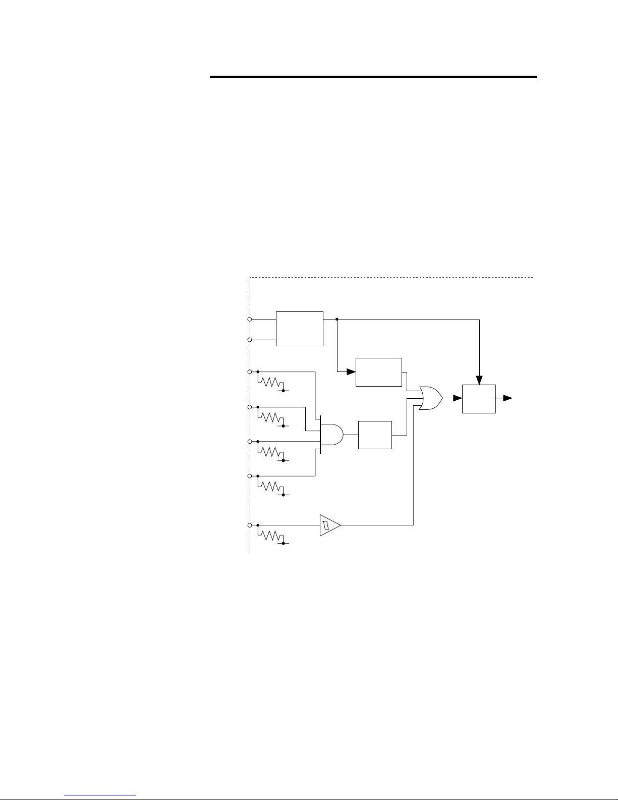
Interrupt and HALT
The E0C6001 Series provide the following interrupt settings,
each of which is maskable.
External interrupt: Input interrupt (one)
Internal interrupt: Timer interrupt (one)
To enable interrupts, the interrupt flag must be set to 1 (EI)
and the necessary related interrupt mask registers must be
set to 1 (enable). When an interrupt occurs, the interrupt
flag is automatically reset to 0 (DI) and interrupts after that
are inhibited.
When a HALT instruction is input, the CPU operating clock
stops and the CPU enters the halt state. The CPU is reactivated from the halt state when an interrupt request occurs.
Figure 4.9.1 shows the configuration of the interrupt circuit.
4.9
Page 59

E0C6001 TECHNICAL HARDWARE
I-52
Fig. 4.9.1 Configuration of interrupt circuit
K00
EIK00
K01
EIK01
K02
EIK02
K03
EIK03
IT2
EIT2
IT8
EIT8
IT32
EIT32
IK0
(MSB)
:
:
(LSB)
Program counter of CPU
(three low-order bits)
Interrupt vector
Interrupt factor flag
Interrupt mask register
Interrupt flag
INT
(Interrupt request)
Page 60

CHAPTER 4: PERIPHERAL CIRCUITS AND OPERATION (Interrupt and HALT)
I-53
Table 4.9.1 shows the factors that generate interrupt requests.
The interrupt factor flags are set to 1 depending on the
corresponding interrupt factors.
The CPU is interrupted when the following two conditions
occur and an interrupt factor flag is set to 1.
• The corresponding mask register is 1 (enabled)
• The interrupt flag is 1 (EI)
The interrupt factor flag is a read-only register, but can be
reset to 0 when the register data is read.
After an initial reset, the interrupt factor flags are reset to 0.
Interrupt factors
Reading of interrupt factor flags is available at EI, but be careful in
the following cases.
If the interrupt mask register value corresponding to the interrupt
factor flags to be read is set to 1, an interrupt request will be
generated by the interrupt factor flags set timing, or an interrupt
request will not be generated. Be very careful when interrupt factor
flags are in the same address.
Note
Table 4.9.1
Interrupt factors
Interrupt Factor
Colck timer 2 Hz falling edge
Colck timer 8 Hz falling edge
Colck timer 32 Hz falling edge
Input data (K00–K03) rising edge
Interrupt Factor Flag
IT2
IT8
IT32
IK0
(0EFH D2)
(0EFH D1)
(0EFH D0)
(0EDH D0)
Page 61

E0C6001 TECHNICAL HARDWARE
I-54
When an interrupt request is input to the CPU, the CPU
begins interrupt processing. After the program being executed is suspended, interrupt processing is executed in the
following order:
➀ The address data (value of the program counter) of the
program step to be executed next is saved on the stack
(RAM).
➁ The interrupt request causes the value of the interrupt
vector (page 1, 01H–07H) to be loaded into the program
counter.
➂ The program at the specified address is executed (execu-
tion of interrupt processing routine).
The processing in steps 1 and 2, above, takes 12 cycles of the
CPU system clock.
Interrupt vectors
Note
The interrupt factor flags can be masked by the corresponding interrupt mask registers. The interrupt mask registers
are read/write registers. They are enabled (interrupt enabled) when 1 is written to them, and masked (interrupt
disabled) when 0 is written to them. After an initial reset,
the interrupt mask register is set to 0.
Table 4.9.2 shows the correspondence between interrupt
mask registers and interrupt factor flags.
Specific masks and
factor flags for interrupt
Table 4.9.2
Interrupt mask registers and
interrupt factor flags
* There is an interrupt mask register for each input port pin.
Interrupt Mask Register
EIT2
EIT8
EIT32
EIK03*
EIK02*
EIK01*
EIK00*
Interrupt Factor Flag
(0EBH D2)
(0EBH D1)
(0EBH D0)
(0E8H D3)
(0E8H D2)
(0E8H D1)
(0E8H D0)
IT2
IT8
IT32
(0EFH D2)
(0EFH D1)
(0EFH D0)
IK0 (0EDH D0)
Page 62

CHAPTER 4: PERIPHERAL CIRCUITS AND OPERATION (Interrupt and HALT)
I-55
Tables 4.9.3 shows the interrupt control bits and their
addresses.
Control of interrupt
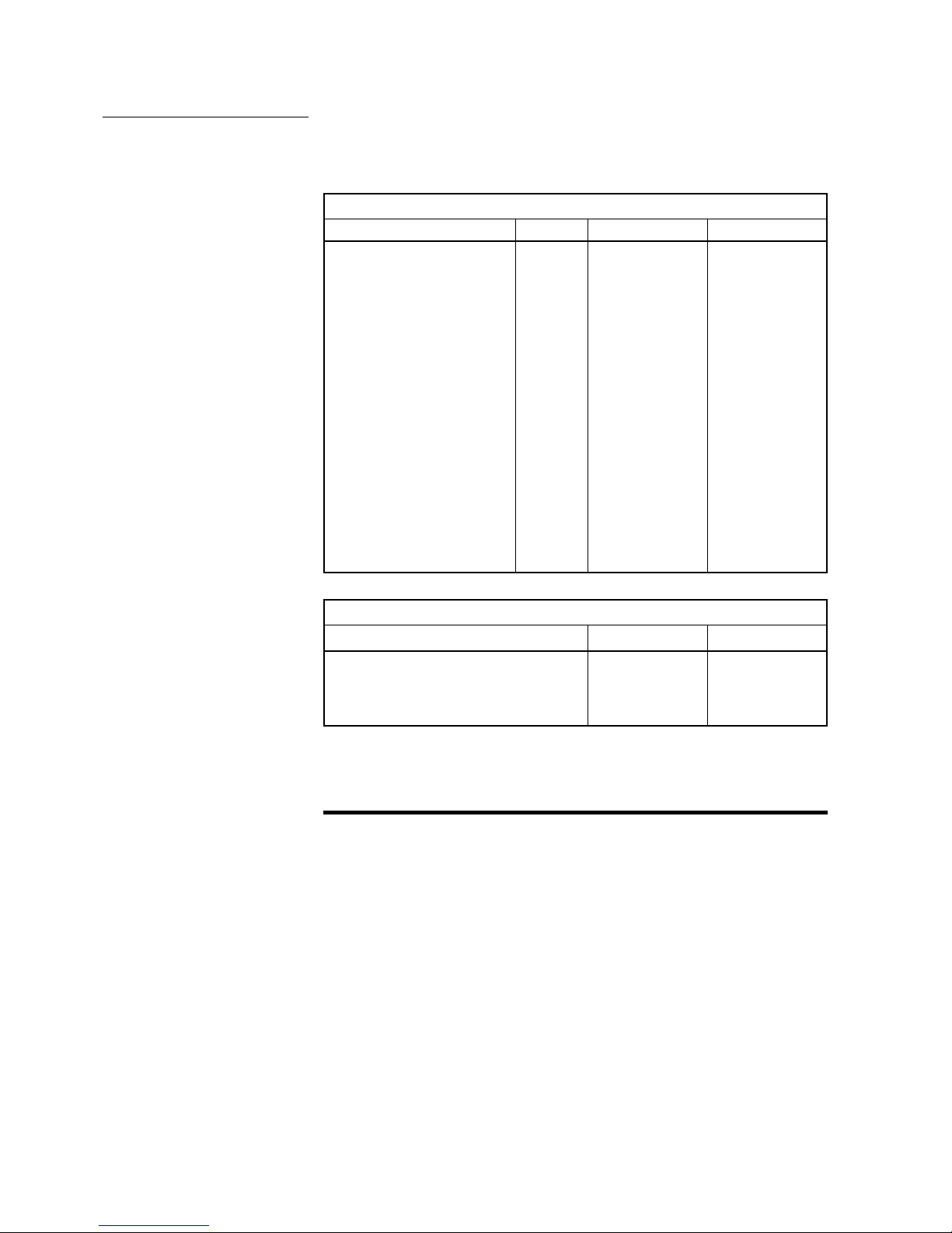
Table 4.9.3 Interrupt control bits
Address Comment
Register
D3 D2 D1 D0 Name SR 1 0
0E8H
0EBH
EIK03 EIK02 EIK01 EIK00
0 EIT2 EIT8 EIT32
R
R/W
EIK03
EIK02
EIK01
EIK00
0
0
0
0
0
EIT2
EIT8
EIT32
0
0
0
Enable
Enable
Enable
Mask
Mask
Mask
Interrupt mask register (K03)
Interrupt mask register (K02)
Interrupt mask register (K01)
Interrupt mask register (K00)
Enable
Enable
Enable
Enable
Mask
Mask
Mask
Mask
Interrupt mask register (clock timer 2 Hz)
Interrupt mask register (clock timer 8 Hz)
Interrupt mask register (clock timer 32 Hz)
R/W
0EDH
0 0 IK0 0
0
0
IK0
0
Interrupt factor flag (K00–K03)
Yes No
0
0EFH
0 IT2 IT8 IT32
0
IT2
IT8
IT32
0
0
0
Enable
Enable
Enable
Mask
Mask
Mask
Interrupt factor flag (clock timer 2 Hz)
Interrupt factor flag (clock timer 8 Hz)
Interrupt factor flag (clock timer 32 Hz)
R
R
Interrupt mask registers (0EBH D0–D2)
Interrupt factor flags (0EFH D0–D2)
See 4.7, "Clock Timer".
Interrupt mask registers (0E8H)
Interrupt factor flag (0EDH D0)
See 4.3, "Input Port".
EIT32, EIT8, EIT2
IT32, IT8, IT2
EIK00–EIK03
IK0
Page 63

E0C6001 TECHNICAL HARDWARE
I-56
BASIC EXTERNAL WIRING DIAGRAM
(1) Piezo Buzzer Single Terminal Driving
CHAPTER 5
X'tal
C
G
C1–C
5
Cp
Crystal oscillator
Trimmer capacitor
Capacitor
Capacitor
32.768 kHz CI(MAX) = 35 kΩ
5–25 pF
0.1 µF
3.3 µF
C1
CG
C5
X'tal
1.5 V
or
3.0 V
Piezo
Buzzer
R01
K00
K03
P00
P03
R00
I
I/O
O
SEG0
SEG19
COM0
COM3
LCD
PANEL
Coil
CA
CB
V
L1
VL2
VL3
VDD
OSC1
OSC2
V
S1
RESET
TEST
V
SS
Cp
Connection depending
on power supply and
LCD panel specification.
Please refer to page I-7.
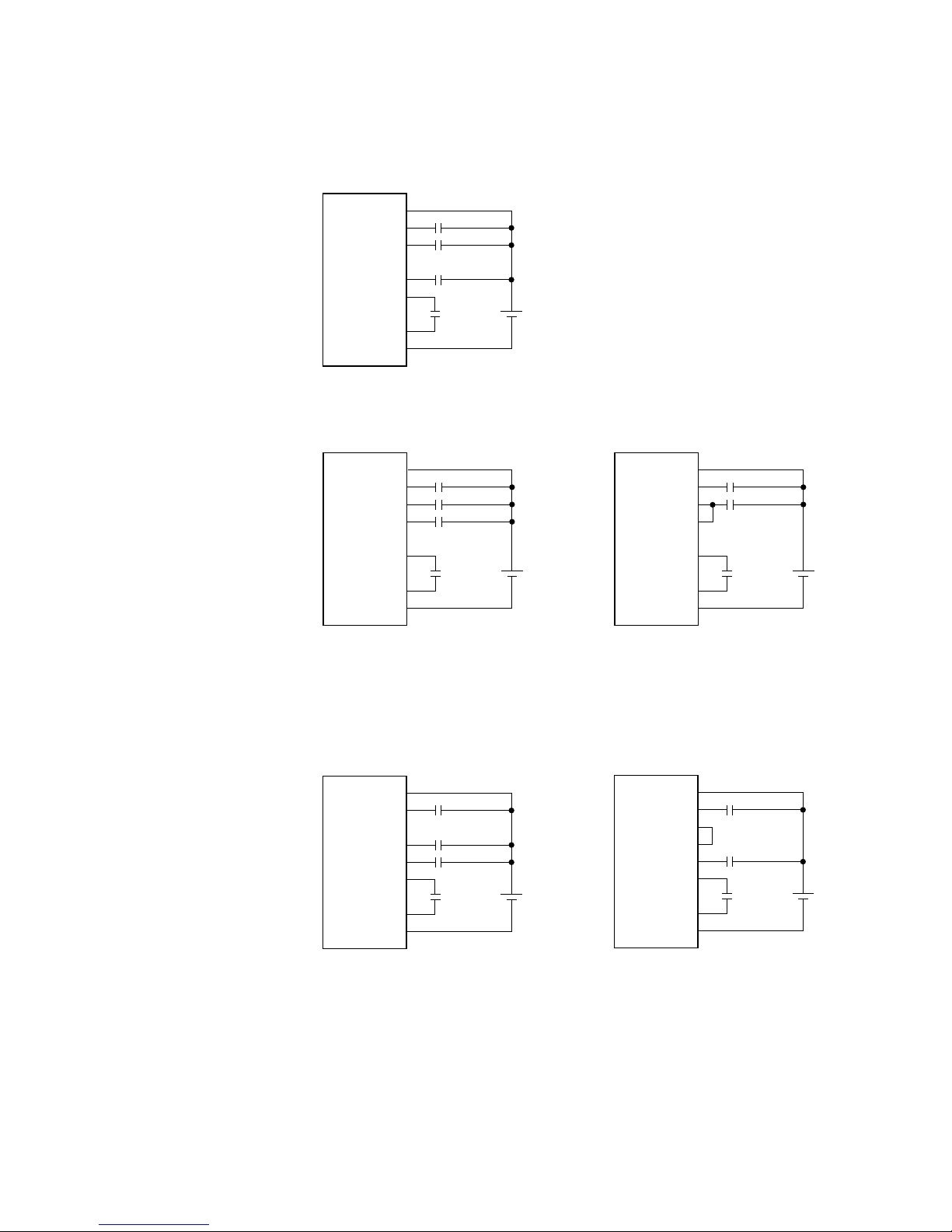
Page 64

CHAPTER 5: BASIC EXTERNAL WIRING DIAGRAM
I-57
(2) Piezo Buzzer Direct Driving
C
1
C
G
C
5
X'tal
I
I/O
SEG0
SEG19
COM0
COM3
LCD
PANEL
CA
CB
V
L1
V
L2
V
L3
V
DD
OSC1
OSC2
V
S1
RESET
TEST
V
SS
Cp
1.5 V
or
3.0 V
Piezo
Buzzer
R01
R00
K00
K03
P00
P03
Connection depending
on power supply and
LCD panel specification.
Please refer to page I-7.
X'tal
C
G
C1–C
5
Cp
Crystal oscillator
Trimmer capacitor
Capacitor
Capacitor
32.768 kHz CI(MAX) = 35 kΩ
5–25 pF
0.1 µF
3.3 µF
Page 65

E0C6001 TECHNICAL HARDWARE
I-58
CHAPTER 6 ELECTRICAL CHARACTERISTICS
6.1 Absolute Maximum Rating
Power voltage
Input voltage (1)
Input voltage (2)
Permissible total output current
*1
Operating temperature
Storage temperature
Soldering temperature / Time
Allowable dissipation
*2
V
SS
V
I
V
IOSC
∑I
VSS
Topr
Tstg
Tsol
P
D
-5.0 to 0.5
Vss-0.3 to 0.5
Vss-0.3 to 0.5
10
-20 to 70
-65 to 150
260°C, 10sec (lead section)
250
V
V
V
mA
°C
°C
–
mW
(VDD=0V)
Item
Symbol Rated Value Unit
∗1 The permissible total output current is the sum total of the
current (average current) that simultaneously flows from the
output pins (or is draw in).
∗2 In case of QFP12-48pin plastic package
Page 66

CHAPTER 6: ELECTRICAL CHARACTERISTICS
I-59
Recommended Operating Conditions
E0C6001
6.2
E0C60L01
Item
Power voltage
Oscillation frequency
Booster capacitor
Capacitor between V
DD
and V
L1
Capacitor between VDD and V
L2
Capacitor between VDD and V
L3
Capacitor between VDD and V
S1
Symbol
V
SS
f
OSC1
f
OSC2
C
1
C
2
C
3
C
4
C
5
Condition
V
DD
=0V
Crystal oscillation
CR oscillation, R=470kΩ
Min
-3.6
50
0.1
0.1
0.1
0.1
0.1
Typ
-3.0
32.768
65
Unit
V
kHz
kHz
µF
µF
µF
µF
µF
Max
-1.8
80
(Ta=-20 to 70°C)
Item
Power voltage
Oscillation frequency
Booster capacitor
Capacitor between V
DD
and V
L1
Capacitor between VDD and V
L2
Capacitor between VDD and V
L3
Capacitor between VDD and V
S1
Symbol
V
SS
f
OSC1
f
OSC2
C
1
C
2
C
3
C
4
C
5
Condition
V
DD
=0V
Crystal oscillation
CR oscillation, R=470kΩ
Min
-2.0
50
0.1
0.1
0.1
0.1
0.1
Typ
-1.5
32.768
65
Unit
V
kHz
kHz
µF
µF
µF
µF
µF
Max
-1.2
80
(Ta=-20 to 70°C)
Page 67

E0C6001 TECHNICAL HARDWARE
I-60
6.3 DC Characteristics
E0C6001
Unless otherwise specified
VDD=0 V, VSS=-3.0 V, fosc=32.768 kHz, Ta=25°C, VS1, VL1, VL2 and VL3 are internal
voltages, and C1=C2=C3=C4=C5=0.1 µF
Item
Symbol
V
IH1
V
IH2
V
IL1
V
IL2
I
IH1
I
IH2
I
IH3
I
IL
I
OH1
I
OH2
I
OL1
I
OL2
I
OH3
I
OL3
I
OH4
I
OL4
I
OH5
I
OL5
Condition Min
0.2•Vss
0.15•Vss
Vss
Vss
0
10
30
-0.5
3.0
3.0
3
3
300
Typ Unit
V
V
V
V
µA
µA
µA
µA
mA
mA
mA
mA
µA
µA
µA
µA
µA
µA
Max
0
0
0.8•Vss
0.85•Vss
0.5
40
100
0
-1.0
-1.0
-3
-3
-300
K00–K03, P00–P03
RESET
K00–K03, P00–P03
RESET
K00–K03, P00–P03
K00–K03
P00–P03, RESET
K00–K03, P00–P03,
RESET, TEST
P00–P03
R00, R01
P00–P03
R00, R01
COM0–COM3
SEG0–SEG19
SEG0–SEG19
High level input voltage (1)
High level input voltage (2)
Low level input voltage (1)
Low level input voltage (2)
High level input current (1)
High level input current (2)
High level input current (3)
Low level input current
High level output current (1)
High level output current (2)
Low level output current (1)
Low level output current (2)
Common output current
Segment output current
(during LCD output)
Segment output current
(during DC output)
V
IH1
=0V
Without pull down resistor
V
IH2
=0V
With pull down resistor
V
IH3
=0V
With pull down resistor
V
IL=VSS
V
OH1
=0.1•V
SS
V
OH2
=0.1•V
SS
(built-in protection resistance)
V
OL1
=0.9•V
SS
V
OL2
=0.9•V
SS
(built-in protection resistance)
V
OH3
=-0.05V
V
OL3=VL3
+0.05V
V
OH4
=-0.05V
V
OL4=VL3
+0.05V
V
OH5
=0.1•V
SS
V
OL5
=0.9•V
SS
Page 68

CHAPTER 6: ELECTRICAL CHARACTERISTICS
I-61
E0C60L01
Unless otherwise specified
VDD=0 V, VSS=-1.5 V, fosc=32.768 kHz, Ta=25°C, VS1, VL1, VL2 and VL3 are internal
voltages, and C1=C2=C3=C4=C5=0.1 µF
Item
Symbol
V
IH1
V
IH2
V
IL1
V
IL2
I
IH1
I
IH2
I
IH3
I
IL
I
OH1
I
OH2
I
OL1
I
OL2
I
OH3
I
OL3
I
OH4
I
OL4
I
OH5
I
OL5
Condition Min
0.2•Vss
0.15•Vss
Vss
Vss
0
5.0
9.0
-0.5
700
700
3
3
130
Typ Unit
V
V
V
V
µA
µA
µA
µA
µA
µA
µA
µA
µA
µA
µA
µA
µA
µA
Max
0
0
0.8•Vss
0.85•Vss
0.5
20
100
0
-200
-200
-3
-3
-100
K00–K03, P00–P03
RESET
K00–K03, P00–P03
RESET
K00–K03, P00–P03
K00–K03
P00–P03, RESET
K00–K03, P00–P03,
RESET, TEST
P00–P03
R00, R01
P00–P03
R00, R01
COM0–COM3
SEG0–SEG19
SEG0–SEG19
High level input voltage (1)
High level input voltage (2)
Low level input voltage (1)
Low level input voltage (2)
High level input current (1)
High level input current (2)
High level input current (3)
Low level input current
High level output current (1)
High level output current (2)
Low level output current (1)
Low level output current (2)
Common output current
Segment output current
(during LCD output)
Segment output current
(during DC output)
V
IH1
=0V
Without pull down resistor
V
IH2
=0V
With pull down resistor
V
IH3
=0V
With pull down resistor
V
IL=VSS
V
OH1
=0.1•V
SS
V
OH2
=0.1•V
SS
(built-in protection resistance)
V
OL1
=0.9•V
SS
V
OL2
=0.9•V
SS
(built-in protection resistance)
V
OH3
=-0.05V
V
OL3=VL3
+0.05V
V
OH4
=-0.05V
V
OL4=VL3
+0.05V
V
OH5
=0.1•V
SS
V
OL5
=0.9•V
SS
Page 69

E0C6001 TECHNICAL HARDWARE
I-62
6.4 Analog Circuit Characteristics and Power Current Consumption
E0C6001 (Normal Operating Mode)
Unless otherwise specified
VDD=0 V, VSS=-3.0 V, fosc=32.768 kHz (crystal oscillation), Ta=25°C, CG=25 pF,
VS1, VL1, VL2 and VL3 are internal voltages, and C1=C2=C3=C4=C5=0.1 µF
E0C6001 (Heavy Load Protection Mode)
Unless otherwise specified
VDD=0 V, VSS=-3.0 V, fosc=32.768 kHz (crystal oscillation), Ta=25°C, CG=25 pF,
VS1, VL1, VL2 and VL3 are internal voltages, and C1=C2=C3=C4=C5=0.1 µF
Item
Internal voltage
Power current
consumption
Symbol
V
L1
V
L2
V
L3
I
OP
Condition
Connect 1MΩ load resistor between V
DD
and V
L1
(without panel load)
Connect 1MΩ load resistor between V
DD
and V
L2
(without panel load)
Connect 1MΩ load resistor between V
DD
and V
L3
(without panel load)
Min
1/2•V
L2
-0.1
3/2•V
L2
-0.1
Typ
V
SS
1.0
2.5
Unit
V
V
V
µA
µA
Max
1/2•V
L2
×
0.9
3/2•V
L2
×
0.9
2.5
5.0
During HALT
During execution
Without panel load
Item
Internal voltage
Power current
consumption
Symbol
V
L1
V
L2
V
L3
I
OP
Condition
Connect 1MΩ load resistor between V
DD
and V
L1
(without panel load)
Connect 1MΩ load resistor between V
DD
and V
L2
(without panel load)
Connect 1MΩ load resistor between V
DD
and V
L3
(without panel load)
Min
1/2•V
L2
-0.1
3/2•V
L2
-0.1
Typ
V
SS
2.0
5.5
Unit
V
V
V
µA
µA
Max
1/2•V
L2
×
0.85
3/2•V
L2
×
0.85
5.5
10.0
During HALT
During execution
Without panel load
Page 70

CHAPTER 6: ELECTRICAL CHARACTERISTICS
I-63
E0C60L01 (Normal Operating Mode)
Unless otherwise specified
VDD=0 V, VSS=-1.5 V, fosc=32.768 kHz (crystal oscillation), Ta=25°C, CG=25 pF,
VS1, VL1, VL2 and VL3 are internal voltages, and C1=C2=C3=C4=C5=0.1 µF
E0C60L01 (Heavy Load Protection Mode)
Unless otherwise specified
VDD=0 V, VSS=-1.5 V, fosc=32.768 kHz (crystal oscillation), Ta=25°C, CG=25 pF,
VS1, VL1, VL2 and VL3 are internal voltages, and C1=C2=C3=C4=C5=0.1 µF
Item
Internal voltage
Power current
consumption
Symbol
V
L1
V
L2
V
L3
I
OP
Condition
Connect 1MΩ load resistor between V
DD
and V
L1
(without panel load)
Connect 1MΩ load resistor between V
DD
and V
L2
(without panel load)
Connect 1MΩ load resistor between V
DD
and V
L3
(without panel load)
Min
2•V
L1
-0.1
3•V
L1
-0.1
Typ
V
SS
1.0
2.5
Unit
V
V
V
µA
µA
Max
2•V
L1
×
0.9
3•V
L1
×
0.9
2.5
5.0
During HALT
During execution
Without panel load
Item
Internal voltage
Power current
consumption
Symbol
V
L1
V
L2
V
L3
I
OP
Condition
Connect 1MΩ load resistor between V
DD
and V
L1
(without panel load)
Connect 1MΩ load resistor between V
DD
and V
L2
(without panel load)
Connect 1MΩ load resistor between V
DD
and V
L3
(without panel load)
Min
2•V
L1
-0.1
3•V
L1
-0.1
Typ
V
SS
2.0
5.5
Unit
V
V
V
µA
µA
Max
2•V
L1
×
0.85
3•V
L1
×
0.85
5.5
10.0
During HALT
During execution
Without panel load
Page 71

E0C6001 TECHNICAL HARDWARE
I-64
E0C6001 (CR, Normal Operating Mode)
Unless otherwise specified
VDD=0 V, VSS=-3.0 V, fosc=65 kHz, Ta=25°C, CG=25 pF, VS1, VL1, VL2 and VL3 are
internal voltages, and C1=C2=C3=C4=C5=0.1 µF, Recommended external resistance
for CR oscillation=470 kΩ
E0C6001 (CR, Heavy Load Protection Mode)
Unless otherwise specified
VDD=0 V, VSS=-3.0 V, fosc=65 kHz, Ta=25°C, CG=25 pF, VS1, VL1, VL2 and VL3 are
internal voltages, and C1=C2=C3=C4=C5=0.1 µF, Recommended external resistance
for CR oscillation=470 kΩ
Item
Internal voltage
Power current
consumption
Symbol
V
L1
V
L2
V
L3
I
OP
Condition
Connect 1MΩ load resistor between V
DD
and V
L1
(without panel load)
Connect 1MΩ load resistor between V
DD
and V
L2
(without panel load)
Connect 1MΩ load resistor between V
DD
and V
L3
(without panel load)
Min
1/2•V
L2
-0.1
3/2•V
L2
-0.1
Typ
V
SS
8.0
15.0
Unit
V
V
V
µA
µA
Max
1/2•V
L2
×
0.9
3/2•V
L2
×
0.9
15.0
20.0
During HALT
During execution
Without panel load
Item
Internal voltage
Power current
consumption
Symbol
V
L1
V
L2
V
L3
I
OP
Condition
Connect 1MΩ load resistor between V
DD
and V
L1
(without panel load)
Connect 1MΩ load resistor between V
DD
and V
L2
(without panel load)
Connect 1MΩ load resistor between V
DD
and V
L3
(without panel load)
Min
1/2•V
L2
-0.1
3/2•V
L1
-0.1
Typ
V
SS
16.0
30.0
Unit
V
V
V
µA
µA
Max
1/2•V
L2
×
0.85
3/2•V
L1
×
0.85
30.0
40.0
During HALT
During execution
Without panel load
Page 72

CHAPTER 6: ELECTRICAL CHARACTERISTICS
I-65
E0C60L01 (CR, Normal Operating Mode)
Unless otherwise specified
VDD=0 V, VSS=-1.5 V, fosc=65 kHz, Ta=25°C, CG=25 pF, VS1, VL1, VL2 and VL3 are
internal voltages, and C1=C2=C3=C4=C5=0.1 µF, Recommended external resistance
for CR oscillation=470 kΩ
E0C60L01 (CR, Heavy Load Protection Mode)
Unless otherwise specified
VDD=0 V, VSS=-1.5 V, fosc=65 kHz, Ta=25°C, CG=25 pF, VS1, VL1, VL2 and VL3 are
internal voltages, and C1=C2=C3=C4=C5=0.1 µF, Recommended external resistance
for CR oscillation=470 kΩ
Item
Internal voltage
Power current
consumption
Symbol
V
L1
V
L2
V
L3
I
OP
Condition
Connect 1MΩ load resistor between V
DD
and V
L1
(without panel load)
Connect 1MΩ load resistor between V
DD
and V
L2
(without panel load)
Connect 1MΩ load resistor between V
DD
and V
L3
(without panel load)
Min
2•V
L1
-0.1
3•V
L1
-0.1
Typ
V
SS
8.0
15.0
Unit
V
V
V
µA
µA
Max
2•V
L1
×
0.9
3•V
L1
×
0.9
15.0
20.0
During HALT
During execution
Without panel load
Item
Internal voltage
Power current
consumption
Symbol
V
L1
V
L2
V
L3
I
OP
Condition
Connect 1MΩ load resistor between V
DD
and V
L1
(without panel load)
Connect 1MΩ load resistor between V
DD
and V
L2
(without panel load)
Connect 1MΩ load resistor between V
DD
and V
L3
(without panel load)
Min
2•V
L1
-0.1
3•V
L1
-0.1
Typ
V
SS
16.0
30.0
Unit
V
V
V
µA
µA
Max
2•V
L1
×
0.85
3•V
L1
×
0.85
30.0
40.0
During HALT
During execution
Without panel load
Page 73

E0C6001 TECHNICAL HARDWARE
I-66
6.5 Oscillation Characteristics
Oscillation characteristics will vary according to different conditions. Use the
following characteristics are as reference values.
E0C6001
Unless otherwise specified
VDD=0 V, VSS=-3.0 V, Crystal : C-002R (CI=35 kΩ), CG=25 pF, CD=built-in, Ta=25°C
E0C60L01
Unless otherwise specified
VDD=0 V, VSS=-1.5 V, Crystal : C-002R (CI=35 kΩ), CG=25 pF, CD=built-in, Ta=25°C
Item
Oscillation start
voltage
Oscillation stop
voltage
Built-in capacity (drain)
Frequency voltage deviation
Frequency IC deviation
Frequency adjustment range
Higher harmonic oscillation
start voltage
Allowable leak resistance
Symbol
Vsta
(Vss)
Vstp
(Vss)
C
D
f/V
f/I
C
f/C
G
V
hho
(Vss)
R
leak
Condition Min
-1.8
-1.8
-10
40
200
Typ
20
Unit
V
V
pF
ppm
ppm
ppm
V
MΩ
Max
5
10
-3.6
t
sta≤5sec
t
stp≤10sec
Including the parasitic capacity inside the IC
Vss=-1.8 to -3.6V
C
G
=5–25pF
C
G
=5pF
Between OSC1 and V
DD
Item
Oscillation start
voltage
Oscillation stop
voltage
Built-in capacity (drain)
Frequency voltage deviation
Frequency IC deviation
Frequency adjustment range
Higher harmonic oscillation
start voltage
Allowable leak resistance
Symbol
Vsta
(Vss)
Vstp
(Vss)
C
D
f/V
f/I
C
f/C
G
V
hho
(Vss)
R
leak
Condition Min
-1.2
-1.2
-10
40
200
Typ
20
Unit
V
V
pF
ppm
ppm
ppm
V
MΩ
Max
5
10
-2.0
t
sta≤5sec
t
stp≤10sec
Including the parasitic capacity inside the IC
Vss=-1.2 to -2.0V
C
G
=5–25pF
C
G
=5pF
Between OSC1 and V
DD
Page 74

CHAPTER 6: ELECTRICAL CHARACTERISTICS
I-67
E0C6001 (CR)
Unless otherwise specified
VDD=0 V, VSS=-3.0 V, RCR=470 kΩ, Ta=25°C
E0C60L01 (CR)
Unless otherwise specified
VDD=0 V, VSS=-1.5 V, RCR=470 kΩ, Ta=25°C
Item
Oscillation frequency dispersion
Oscillation start voltage
Oscillation start time
Oscillation stop voltage
Symbol
fosc
Vsta
t
sta
Vstp
Condition
Vss=-1.8 to -3.6V
Min
-20
-1.8
-1.8
Typ
65kHz
3
Unit
%
V
ms
V
Max
20
Item
Oscillation frequency dispersion
Oscillation start voltage
Oscillation start time
Oscillation stop voltage
Symbol
fosc
Vsta
t
sta
Vstp
Condition
Vss=-1.2 to -2.0V
Min
-20
-1.2
-1.2
Typ
65kHz
3
Unit
%
V
ms
V
Max
20
Page 75

E0C6001 TECHNICAL HARDWARE
I-68
CHAPTER 7 PACKAGE
7.1 Plastic Package
Plastic QFP12-48pin
7
±0.1
9
±0.4
2536
7
±0.19±0.4
13
24
INDEX
0.18
121
48
37
1.4
±0.1
0.1
1.7
max
1
0.5
±0.2
0°
10°
0.125
±0.05
0.5
+0.1
–0.05
Page 76

CHAPTER 7: PACKAGE
I-69
7.2
Ceramic Package for Test Samples
DIP-64pin
Pin No.
1
2
3
4
5
6
7
8
9
10
11
12
13
14
15
16
Pin Name
N.C.
SEG5
SEG4
SEG3
SEG2
SEG1
SEG0
N.C.
N.C.
N.C.
COM0
COM1
COM2
COM3
V
L3
V
L2
Pin No.
17
18
19
20
21
22
23
24
25
26
27
28
29
30
31
32
Pin Name
V
L1
CA
CB
V
SS
V
DD
OSC1
OSC2
N.C.
N.C.
V
S1
N.C.
N.C.
N.C.
P00
P01
P02
Pin No.
33
34
35
36
37
38
39
40
41
42
43
44
45
46
47
48
Pin Name
P03
K00
K01
K02
K03
N.C.
N.C.
N.C.
N.C.
N.C.
R01
R00
SEG19
SEG18
SEG17
SEG16
Pin No.
49
50
51
52
53
54
55
56
57
58
59
60
61
62
63
64
N.C. = No Connection
Pin Name
SEG15
SEG14
SEG13
SEG12
SEG11
SEG10
N.C.
N.C.
N.C.
TEST
RESET
SEG9
SEG8
SEG7
SEG6
N.C.
12Pin No.
Index Mark
3132
64 63 3433
81.3
78.7
23.1
2.54
22.8
(Unit: mm)
Page 77

E0C6001 TECHNICAL HARDWARE
I-70
CHAPTER 8
8.1
PAD LAYOUT
Diagram of Pad Layout
Chip size: 2,640 µm (X) x 2,180 µm (Y)
Y
X
(0, 0)
1510
15
20
25 30 35
40
45
Die No.
Page 78

CHAPTER 8: PAD LAYOUT
I-71
8.2 Pad Coordinates
(Unit: µm)
Pad No
1
2
3
4
5
6
7
8
9
10
11
12
13
14
15
16
17
18
19
20
21
22
23
Pad No
24
25
26
27
28
29
30
31
32
33
34
35
36
37
38
39
40
41
42
43
44
45
46
Pad Name
R01
R00
SEG19
SEG18
SEG17
SEG16
SEG15
SEG14
SEG13
SEG12
SEG11
SEG10
TEST
RESET
SEG9
SEG8
SEG7
SEG6
SEG5
SEG4
SEG3
SEG2
SEG1
Pad Name
SEG0
COM0
COM1
COM2
COM3
V
L3
V
L2
V
L1
CA
CB
V
SS
V
DD
OSC1
OSC2
V
S1
P00
P01
P02
P03
K00
K01
K02
K03
X
759
629
401
271
141
11
-119
-249
-379
-509
-639
-769
-1,151
-1,151
-1,151
-1,151
-1,151
-1,151
-1,151
-1,151
-1,151
-1,151
-1,151
X
-1,151
-1,126
-988
-858
-727
-597
-466
-336
-206
-76
570
700
835
987
1,140
1,151
1,151
1,151
1,151
1,151
1,151
1,151
1,151
Y
923
923
923
923
923
923
923
923
923
923
923
923
789
657
526
396
266
136
6
-124
-254
-384
-514
Y
-644
-923
-923
-923
-923
-923
-923
-923
-923
-923
-923
-923
-923
-923
-923
-11
119
249
379
518
648
778
908
Page 79

Software
E0C6001
II.
Technical Software
Page 80

Software
CONTENTS
CHAPTER 1 CONFIGURATION ........................................................... II-1
1.1 E0C6001 Block Diagram ................................................ II-1
1.2 ROM Map ....................................................................... II-2
1.3 Interrupt Vectors............................................................. II-3
1.4 Data Memory Map.......................................................... II-4
CHAPTER 2 INITIAL RESET ................................................................... II-9
2.1 Internal Register Status on Initial Reset ......................... II-9
2.2 Initialize Program Example............................................ II-11
CHAPTER 3 PERIPHERAL CIRCUITS.................................................... II-13
3.1 Input Port....................................................................... II-13
Input port memory map .......................................... II-13
Control of the input port ......................................... II-14
Examples of input port control program .................. II-14
3.2 Output Port .................................................................... II-16
Output port memory map........................................ II-16
Control of the output port ....................................... II-16
Examples of output port control program ................ II-17
3.3 Special Use Output Port................................................ II-19
Special use output port memory map ...................... II-19
Control of the special use output port ..................... II-20
Examples of special use output port
control program ...................................................... II-21
Page 81

3.4 I/O Port .......................................................................... II-23
I/O port memory map ............................................. II-23
Control of the I/O port ............................................ II-24
Examples of I/O port control program ..................... II-25
3.5 LCD Driver..................................................................... II-28
LCD driver memory map ......................................... II-28
Control of the LCD driver ........................................ II-29
Examples of LCD driver control program ................. II-31
3.6 Timer ............................................................................. II-33
Timer memory map ................................................. II-33
Control of the timer................................................. II-34
Examples of timer control program.......................... II-35
3.7 Heavy Load Protection Function ................................... II-37
Heavy load protection function memory map ........... II-37
Heavy load protection function ................................ II-37
Examples of heavy load protection
function control program......................................... II-38
3.8 Interrupt and Halt........................................................... II-39
Interrupt memory map ............................................ II-39
Control of interrupts and halt ................................. II-40
Examples of interrupt and halt control program ...... II-48
CHAPTER 4 SUMMARY OF PROGRAMMING POINTS....................... II-50
APPENDIX A Table of Instructions...................................................... II-54
B The E0C6001 I/O Memory Map .................................... II-59
C Table of the ICE6200 Commands ................................. II-60
D Cross-assembler Pseudo-instruction List ...................... II-62
Page 82

CHAPTER 1: CONFIGURATION
II-1
CHAPTER 1
1.1
CONFIGURATION
E0C6001 Block Diagram
Power
Controller
LCD
Driver
RAM
80
×
4
Interrupt
Generator
I Port
Test Port
I/O Port
O Port
Timer
Core CPU E0C6200B
ROM
1,024 × 12
OSC
System
Reset
Control
RESET
OSC1
COM0
|
COM3
SEG0
|
SEG19
V
DD
V
L1
|
V
L3
CA
CB
V
S1
V
SS
K00~K03
TEST
P00~P03
R00, R01
OSC2
FOUT
&
BUZZER
(FOUT/BUZZER)
(BUZZER)
Fig. 1.1.1
E0C6001 block diagram
Page 83

E0C6001 TECHNICAL SOFTWARE
II-2
ROM Map
The E0C6001 has a built-in mask ROM with a capacity of
1,024 steps × 12 bits for program storage. The configuration
of the ROM is shown in Figure 1.2.1.
1.2
Fig. 1.2.1
Configuration of built-in ROM
00H step
07H step
08H step
FFH step
12 bits
Program start address
Interrupt vector area
Bank 0
Program area
0 page
1 page
2 page
3 page
01H step
Page 84

CHAPTER 1: CONFIGURATION
II-3
Interrupt Vectors
When an interrupt request is received by the CPU, the CPU
initiates the following interrupt processing after completing
the instruction being executed.
(1)The address of the next instruction to be executed (the
value of the program counter) is saved on the stack
(RAM).
(2)The interrupt vector address corresponding to the inter-
rupt request is loaded into the program counter.
(3)The branch instruction written in the vector is executed
to branch to the software interrupt processing routine.
Steps 1 and 2 require 12 cycles of the CPU system clock.
The interrupt vectors are shown in Table 1.3.1.
1.3
Note
Table 1.3.1
Interrupt requests and vectors
Addesses (start address of interrupt processing routines) to
jump to are written into the addresses available for interrupt
vector allocation.
Step Interrupt Vector
Initial reset
Clock timer interrupt
Input (K00–K03) interrupt
Input interrupt and clock timer interrupt
Page
00H
01H
04H
05H
1
Page 85

E0C6001 TECHNICAL SOFTWARE
II-4
Data Memory Map
The E0C6001 built-in RAM has 80 words of data memory,
32 words of display memory for the LCD, and I/O memory
for controlling the peripheral circuit. When writing programs, note the following:
(1)Since the stack area is in the data memory area, take
care not to overwrite the stack with data. Subroutine
calls or interrupts use 3 words on the stack.
(2)Data memory addresses 000H–00FH are memory register
areas that are addressed with register pointer RP.
Fig. 1.4.1
Data memory map
1.4
Address
Page High
Low
0123456789ABCDE
F
M0 M1 M2 M3 M4 M5 M6 M7 M8 M9 MA MB MC MD ME MF
3
0
1
2
4
5
6
7
8
9
A
B
C
D
E
F
0
RAM (80 words x 4 bits)
R/W
Unused area
I/O memory
Display memory
Unused area
Memory is not mounted in unused area within the memory map
and in memory area not indicated in this chapter. For this reason,
normal operation cannot be assured for programs that have been
prepared with access to these areas.
Note
Page 86

CHAPTER 1: CONFIGURATION
II-5
Table 1.4.1(a) I/O memory map 1
*1 Initial value following initial reset
*2 Not set in the circuit
*3 Undefined
*4 Reset (0) immediately after being read
*5 Always 0 when being read
*6 Refer to main manual
Address Comment
Register
D3 D2 D1 D0 Name SR
*1
10
0E0H
0E4H
0E8H
K03 K02 K01 K00
TM3 TM2 TM1 TM0
EIK03 EIK02 EIK01 EIK00
R/W
R
R
K03
K02
K01
K00
–
–
–
–
TM3
TM2
TM1
TM0
–
–
–
–
EIK03
EIK02
EIK01
EIK00
0
0
0
0
Enable
Enable
Enable
Enable
Mask
Mask
Mask
Mask
Timer data (clock timer 2 Hz)
Timer data (clock timer 4 Hz)
Timer data (clock timer 8 Hz)
Timer data (clock timer 16 Hz)
Input port (K00–K03)
High
High
High
High
Low
Low
Low
Low
Interrupt mask register (K03)
Interrupt mask register (K02)
Interrupt mask register (K01)
Interrupt mask register (K00)
High
High
High
High
Low
Low
Low
Low
*2
*2
*2
*2
0 EIT2 EIT8 EIT32 0
EIT2
EIT8
EIT32
0
0
0
Interrupt mask register (clock timer 2 Hz)
Interrupt mask register (clock timer 8 Hz)
Interrupt mask register (clock timer 32 Hz)
Enable
Enable
Enable
Mask
Mask
Mask
0EBH
R R/W
*5
Page 87

E0C6001 TECHNICAL SOFTWARE
II-6
Table 1.4.1(b) I/O memory map 2
*1 Initial value following initial reset
*2 Not set in the circuit
*3 Undefined
*4 Reset (0) immediately after being read
*5 Always 0 when being read
*6 Refer to main manual
Address Comment
Register
D3 D2 D1 D0 Name SR
*1
10
0EDH
0EFH
0 0 0 IK0
0 IT2 IT8 IT32
0
0
0
IK0
0
0
IT2
IT8
IT32
0
0
0
Yes
Yes
Yes
Interrupt factor flag (K00–K03)
Interrupt factor flag (clock timer 2 Hz)
Interrupt factor flag (clock timer 8 Hz)
Interrupt factor flag (clock timer 32 Hz)
Yes No
R
R
*5
*5
*5
*4
0F6H
P03 P02 P01 P00
P03
P02
P01
P00
–
–
–
–
I/O port (P00–P03)
High
High
High
High
Low
Low
Low
Low
*2
*2
*2
*2
R/W
*5
*4
*4
*4
*5
*5
No
No
No
0F3H
00
R01 R00
0
0
R01
BUZZER
R00
FOUT
0
0
0
0
High
ON
High
ON
Low
OFF
Low
OFF
R01 output port data
Buzzer ON/OFF control register
R00 output port data
Frequency output ON/OFF control register
R/WR
BUZZER FOUT
Page 88

CHAPTER 1: CONFIGURATION
II-7
Table 1.4.1(c) I/O memory map 3
*1 Initial value following initial reset
*2 Not set in the circuit
*3 Undefined
*4 Reset (0) immediately after being read
*5 Always 0 when being read
*6 Refer to main manual
Address Comment
Register
D3 D2 D1 D0 Name SR
*1
10
0F9H
0FAH
0 TMRST 0 0
HLMOD 0 0 0
W
0
TMRST
0
0
Reset
HLMOD
0
0
0
0
Clock timer reset
Heavy load protection mode register
Reset –
R
RR
R/W
Heavy
load
Normal
load
*5
*5
*5
0FBH
0FCH
CSDC 0 0 0
0 0 0 IOC
R
R
0
0
0
0
IOC
0
I/O port P00–P03 Input/Output
LCD drive switch
Static Dynamic
Output Input
*5
*5
*5
*5
*5
*5
R/W
R/W
CSDC
0
0
0
*5
*5
*5
Page 89

E0C6001 TECHNICAL SOFTWARE
II-8
Table 1.4.1(d) I/O memory map 4
*1 Initial value following initial reset
*2 Not set in the circuit
*3 Undefined
*4 Reset (0) immediately after being read
*5 Always 0 when being read
*6 Refer to main manual
Address Comment
Register
D3 D2 D1 D0 Name SR
*1
10
0FDH
XBZR 0 XFOUT1 XFOUT0RXBZR
0
XFOUT1
XFOUT0
0
0
0
Buzzer frequency control
2 kHz
High
High
4 kHz
Low
Low
R/WR/W
*5
FOUT frequency control:
XFOUT1(0), XFOUT0(0) -> F1
XFOUT1(0), XFOUT0(1) -> F2
XFOUT1(1), XFOUT0(0) -> F3
XFOUT1(1), XFOUT0(1) -> F4
Page 90

CHAPTER 2: INITIAL RESET
II-9
INITIAL RESET
Internal Register Status on Initial Reset
Following an initial reset, the internal registers and internal
data memory area are initialized to the values shown in
Tables 2.1.1 and 2.1.2.
Internal Register Bit Length Initial Value Following Reset
Program counter step PCS 8 00H
Program counter page PCP 4 1H
New page pointer NPP 4 1H
Stack pointer SP 8 Undefined
Index register X 8 Undefined
Index register Y 8 Undefined
Register pointer RP 4 Undefined
General register A 4 Undefined
General register B 4 Undefined
Interrupt flag I 1 0
Decimal flag D 1 0
Zero flag Z 1 Undefined
Carry flag C 1 Undefined
Internal Data Initial Value
Memory Area Following Reset
RAM data 4 × 80 Undefined 000H–05FH
Display memory 4 × 20 Undefined 090H–0AFH
Internal I/O register See Tables 1.4.1(a)–1.4.1(d) 0E0H–0FDH
2.1
Table 2.1.1
Initial values of internal
registers
CHAPTER 2
Table 2.1.2
Initial values of internal data
memory area
Bit Length Address
Page 91

E0C6001 TECHNICAL SOFTWARE
II-10
After an initial reset, the program counter page (PCP) is
initialized to 1H, and the program counter step (PCS), to
00H. This is why the program is executed from step 00H of
the first page.
The initial values of some internal registers and internal
data memory area locations are undefined after a reset. Set
them as necessary to the proper initial values in the program.
The peripheral I/O functions (memory-mapped I/O) are
assigned to internal data memory area addresses 0E0H to
0FDH. Each address represents a 4-bit internal I/O register,
allowing access to the peripheral functions in 1-word (4-bit)
read/write units.
Page 92

CHAPTER 2: INITIAL RESET
II-11
Initialize Program Example
The following is a program that clears the RAM and LCD,
resets the flags, registers and timer, and sets the stack
pointer immediately after resetting the system.
Label Mnemonic/operand Comment
ORG 100H
JP INIT ;Jump to "INIT"
;
ORG 110H
INIT RST F,0011B ;Interrupt mask, decimal
;adjustment off
;
LD X,0 ;
RAMCLR LDPX MX,0 ;
CP XH,5H ;
JP NZ,RAMCLR ;
LD X,90H ;
LCDCLR LDPX MX,0 ;
CP XH,0BH ;
JP NZ,LCDCLR ;
;
LD A,0 ;
LD B,4 ;
LD SPL,A ;
LD SPH,B ;
;
LD X,0F9H ;
OR MX,0100B ;
;
LD X,0EBH ;
OR MX,0111B ;
;
LD X,0E8H ;
OR MX,1111B ;
;
LD X,0 ;
LD Y,0 ;
LD A,0 ;
LD B,0 ;
RST F,0 ;
EI ;Enable interrupt
Clear RAM (00H–4FH)
Enable timer interrupt
Enable input interrupt
(K03–K00)
Clear LCD (90H–AFH)
Reset timer
Set stack pointer to 40H
2.2
Reset register flags
Page 93

E0C6001 TECHNICAL SOFTWARE
II-12
The above program is a basic initialization program for the
E0C6001. The setting data are all initialized as shown in
Table 2.1.1 by executing this program. When using this
program, add setting items necessary for each specific
application. (Figure 2.2.1 is the flow chart for this program.)
Fig. 2.2.1
Flow chart of the initialization
program
Initialization
Reset
I (Interrupt flag)
D (Decimal adjustment flag)
Clear RAM
Set SP
Reset timer
Enable timer interrupt
Enable input interrupt
Reset registers (X, Y, A, B)
flags (I, Z, D, C)
EI (enable interrupt)
I : Interrupt flag
D : Decimal adjustment flag
Clear data RAM (00H to 04FH)
Clear segment RAM (90H to 0AFH)
Set stack pointer to 40H
Enable K03–K00 input port interrupt
Enable timer interrupt 2 Hz, 8 Hz, 32 Hz
To next process
Page 94

CHAPTER 3: PERIPHERAL CIRCUITS (Input Port)
II-13
PERIPHERAL CIRCUITS
Details on how to control the E0C6001 peripheral circuit is
given in this chapter.
CHAPTER 3
3.1
Input port memory
map
Table 3.1.1 I/O memory map
*1 Initial value following initial reset
*2 Not set in the circuit
*3 Undefined
*4 Reset (0) immediately after being read
*5 Always 0 when being read
*6 Refer to main manual
Input Port
Address Comment
Register
D3 D2 D1 D0 Name SR
*1
10
0E0H
K03 K02 K01 K00
R
K03
K02
K01
K00
–
–
–
–
Input port (K00–K03)
High
High
High
High
Low
Low
Low
Low
*2
*2
*2
*2
0E8H
EIK03 EIK02 EIK01 EIK00
R/W
EIK03
EIK02
EIK01
EIK00
0
0
0
0
Interrupt mask register (K03)
Interrupt mask register (K02)
Interrupt mask register (K01)
Interrupt mask register (K00)
Enable
Enable
Enable
Enable
Mask
Mask
Mask
Mask
0EDH
0 0 IK0
R
0
0
0
IK0
0
Interrupt factor flag (K00–K03)
Yes No
*5
*5
*5
*4
0
Page 95

E0C6001 TECHNICAL SOFTWARE
II-14
The E0C6001 has one 4-bit input port (K00–K03). Input port
data can be read as a 4-bit unit (K00–K03).
The state of the input ports can be obtained by reading the
data (bits D3, D2, D1, D0) of address 0E0H. The input ports
can be used to send an interrupt request to the CPU via the
input interrupt condition flag. See Section 3.8 "Interrupt
and Halt", for details.
• Loading K00–K03 into the A register
Label Mnemonic/operand Comment
LD Y,0E0H ;Set address of port
LD A,MY ;A register ← K00–K03
As shown in Figure 3.1.1, the two instruction steps above
load the data of the input port into the A register.
Control of
the input port
Examples of input
port control
program
D3
K03D2K02D1K01D0K00
A register
The data of the input port can be loaded into the B register
or MX instead of the A register.
Fig. 3.1.1
Loading the A register
Page 96

CHAPTER 3: PERIPHERAL CIRCUITS (Input Port)
II-15
• Bit-unit checking of input ports
Label Mnemonic/operand Comment
DI ;Disable interrupt
LD Y,0E0H ;Set address of port
INPUT1: FAN MY,0010B ;
JP NZ,INPUT1 ;Loop until K01 becomes "0"
INPUT2: FAN MY,0010B ;
JP Z,INPUT2 ;Loop until K01 becomes "1"
This program loopes until a rising edge is input to input port
K01.
The input port can be addressed using the X register instead
of the Y register.
When the input port is changed from high level to low level with a
pull-down resistor, the signal falls following a certain delay caused
by the time constants of the pull-down resistance and the input
gate capacitance. It is therefore necessary to observe a proper
wait time before the input port data is read.
Note
Page 97

E0C6001 TECHNICAL SOFTWARE
II-16
Output Port3.2
Output port
memory map
Table 3.2.1 I/O memory map
*1 Initial value following initial reset
*2 Not set in the circuit
*3 Undefined
*4 Reset (0) immediately after being read
*5 Always 0 when being read
*6 Refer to main manual
The E0C6001 Series have 2 bits for general output ports
(R00, R01). R00 and R01 although can be use for special
use output port as shown in later of this section. The output
port is a read/write register, output pins provide the contents of the register. The states of the output ports (R00,
R01) are decided by the data of address 0F3H. Output ports
can also be read, and output control is possible using the
operation instructions (AND, OR, etc.). The output ports are
all initialized to low level (0) after an initial reset.
Control of
the output port
Address Comment
Register
D3 D2 D1 D0 Name 1 0
0F3H
00
R01 R00
0
0
R01
BUZZER
R00
FOUT
0
0
0
0
High
ON
High
ON
Low
OFF
Low
OFF
R01 output port data
Buzzer ON/OFF control register
R00 output port data
Frequency output ON/OFF control register
R/WR
BUZZER FOUT
*5
*5
SR
*1
Page 98

CHAPTER 3: PERIPHERAL CIRCUITS (Output Port)
II-17
• Loading B register data into R00, R01
Label Mnemonic/operand Comment
LD Y,0F3H ;Set address of port
LD MY,B ;R00, R01 ← B register
As shown in Figure 3.2.1, the two instruction steps above
load the data of the B register into the output ports.
Examples of output
port control
program
D3 D2 D1 D0
Data register
R00
Data register
R01
B register
"0" when being read
"0" when being read
Fig. 3.2.1
Control of the output port
The output data can be taken from the A register, MX, or
immediate data instead of the B register.
Page 99

E0C6001 TECHNICAL SOFTWARE
II-18
• Bit-unit operation of output ports
Label Mnemonic/operand Comment
LD Y,0F3H ;Set address of port
OR MY,0010B ;Set R01 to 1
AND MY,1110B ;Set R00 to 0
The three instruction steps above cause the output port to
be set, as shown in Figure 3.2.2.
Fig. 3.2.2
Setting of the output port
0 0 R01 R00
Sets "0"
Sets "1"
Unused
Unused
Address 0F3H
D3 D2 D1 D0
Page 100

CHAPTER 3: PERIPHERAL CIRCUITS (Special Use Output Port)
II-19
Special Use Output Port3.3
Special use output
port memory map
Table 3.3.1 I/O memory map
*1 Initial value following initial reset
*2 Not set in the circuit
*3 Undefined
*4 Reset (0) immediately after being read
*5 Always 0 when being read
*6 Refer to main manual
Address Comment
Register
D3 D2 D1 D0 Name 1 0
0F3H
00
R01 R00
0
0
R01
BUZZER
R00
FOUT
0
0
0
0
High
ON
High
ON
Low
OFF
Low
OFF
R01 output port data
Buzzer ON/OFF control register
R00 output port data
Frequency output ON/OFF control register
R/WR
BUZZER FOUT
0FDH
XBZR 0 XFOUT1 XFOUT0RXBZR
0
XFOUT1
XFOUT0
0
0
0
Buzzer frequency control
2 kHz
High
High
4 kHz
Low
Low
R/WR/W
FOUT frequency control:
XFOUT1(0), XFOUT0(0) -> F1
XFOUT1(0), XFOUT0(1) -> F2
XFOUT1(1), XFOUT0(0) -> F3
XFOUT1(1), XFOUT0(1) -> F4
*5
*5
SR
*1
*5
 Loading...