

Page 1
Denon Brand Company, D&M Holdings lnc.
e
Ver. 3
●
For purposes of improvement, specifications and
design are subject to change without notice.
●
Please use this service manual with referring to the
operating instructions without fail.
●
Some illustrations using in this service manual are
slightly different from the actual set.
注 意
サービスをおこなう前に、このサービスマニュアル
を必ずお読みください。本機は、火災、感電、けが
などに対する安全性を確保するために、さまざまな
配慮をおこなっており、また法的には「電気用品安
全法」にもとづき、所定の許可を得て製造されてお
ります。従ってサービスをおこなう際は、これらの
安全性が維持されるよう、このサービスマニュアル
に記載されている注意事項を必ずお守りください。
●
本機の仕様は性能改良のため、予告なく変更すること
があります。
●
補修用性能部品の保有期間は、製造打切後 8 年です。
●
修理の際は、必ず取扱説明書を参照の上、作業を行っ
てください。
●
本文中に使用しているイラストは、説明の都合上現物
と多少異なる場合があります。
Please refer to the
MODIFICATION NOTICE.
SERVICE MANUAL
MODEL JP E3 E2 EK E2A E1C E1K EUT
DVD-3800BDCI
BLU-RAY DISC/DVD VIDEO PLAYER
3
X0380 V.03 DE/CDM 0902
Page 2

SAFETY PRECAUTIONS
The following check should be performed for the continued protection of the customer and service technician.
LEAKAGE CURRENT CHECK
Before returning the unit to the customer, make sure you make either (1) a leakage current check or (2) a line to chassis
resistance check. If the leakage current exceeds 0.5 milliamps, or if the resistance from chassis to either side of the
power cord is less than 460 kohms, the unit is defective.
LASER RADIATION
Caution - Class 1M visible and invisible laser radiation when open.
Do not view directly with optical instruments.
CAUTION
Please heed the points listed below during servicing and inspection.
◎ Heed the cautions!
Spots requiring particular attention when servicing, such
as the cabinet, parts, chassis, etc., have cautions indicated
on labels or seals. Be sure to heed these cautions and the
cautions indicated in the handling instructions.
◎ Caution concerning electric shock!
(1) An AC voltage is impressed on this set, so touching in-
ternal metal parts when the set is energized could
cause electric shock. Take care to avoid electric shock,
by for example using an isolating transformer and
gloves when servicing while the set is energized, unplugging the power cord when replacing parts, etc.
(2)There are high voltage parts inside. Handle with extra
care when the set is energized.
◎ Caution concerning disassembly and
assembly!
Though great care is taken when manufacturing parts from
sheet metal, there may in some rare cases be burrs on the
edges of parts which could cause injury if fingers are
moved across them. Use gloves to protect your hands.
◎ Inspect for safety after servicing!
Check that all screws, parts and wires removed or disconnected for servicing have been put back in their original positions, inspect that no parts around the area that has been
serviced have been negatively affected, conduct an insulation check on the external metal connectors and between
the blades of the power plug, and otherwise check that
safety is ensured.
(Insulation check procedure)
Unplug the power cord from the power outlet, disconnect
the antenna, plugs, etc., and turn the power switch on. Using a 500V insulation resistance tester, check that the insulation resistance between the terminals of the power
plug and the externally exposed metal parts (antenna terminal, headphones terminal, microphone terminal, input
terminal, etc.) is 1MΩ or greater. If it is less, the set must
be inspected and repaired.
CAUTION
Concerning important safety
parts
◎ Only use designated parts!
The set's parts have specific safety properties (fire resistance, voltage resistance, etc.). For replacement parts, be
sure to use parts which have the same properties. In particular, for the important safety parts that are marked z on
wiring diagrams and parts lists, be sure to use the designated parts.
◎ Be sure to mount parts and arrange
the wires as they were originally!
For safety reasons, some parts use tape, tubes or other insulating materials, and some parts are mounted away from
the surface of printed circuit boards. Care is also taken with
the positions of the wires inside and clamps are used to
keep wires away from heating and high voltage parts, so
be sure to set everything back as it was originally.
DVD-3800BDCI
Many of the electric and structural parts used in the set
have special safety properties. In most cases these properties are difficult to distinguish by sight, and using replacement parts with higher ratings (rated power and
withstand voltage) does not necessarily guarantee that
safety performance will be preserved. Parts with safety
properties are indicated as shown below on the wiring diagrams and parts lists is this service manual. Be sure to replace them with parts with the designated part number.
(1) Schematic diagrams ... Indicated by the z mark.
(2) Parts lists ... Indicated by the z mark.
Using parts other than the designated
parts could result in electric shock, fires or
other dangerous situations.
2
Page 3
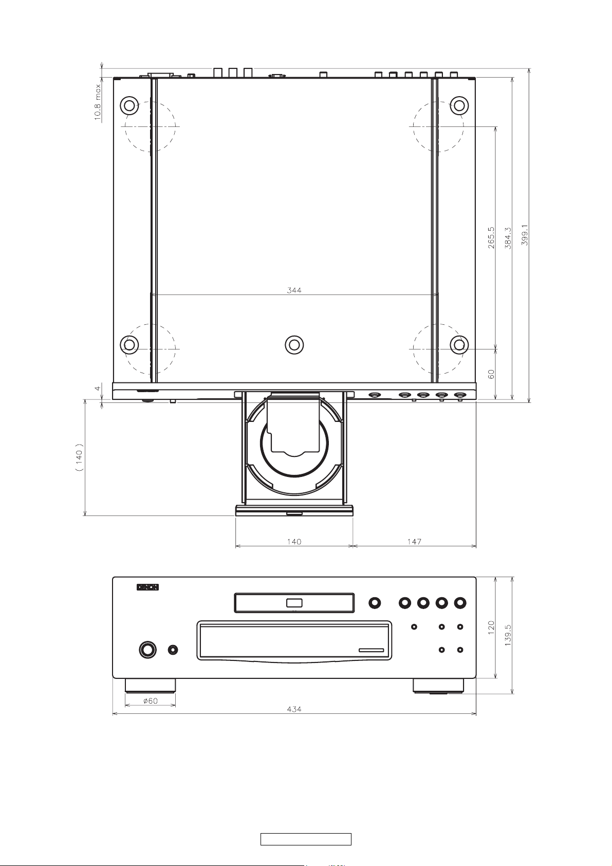
DIMENSION
3
DVD-3800BDCI
Page 4
WIRE ARRANGEMENT
If wire bundles are untied or moved to perform adjustment or parts replacement etc., be sure to rearrange
them neatly as they were originally bundled or placed afterward.
Otherwise, incorrect arrangement can be a cause of noise generation.
Wire arrangement viewed from the top
4
DVD-3800BDCI
Page 5
SPECIFICATIONS
5
DVD-3800BDCI
Page 6
6
DVD-3800BDCI
Page 7
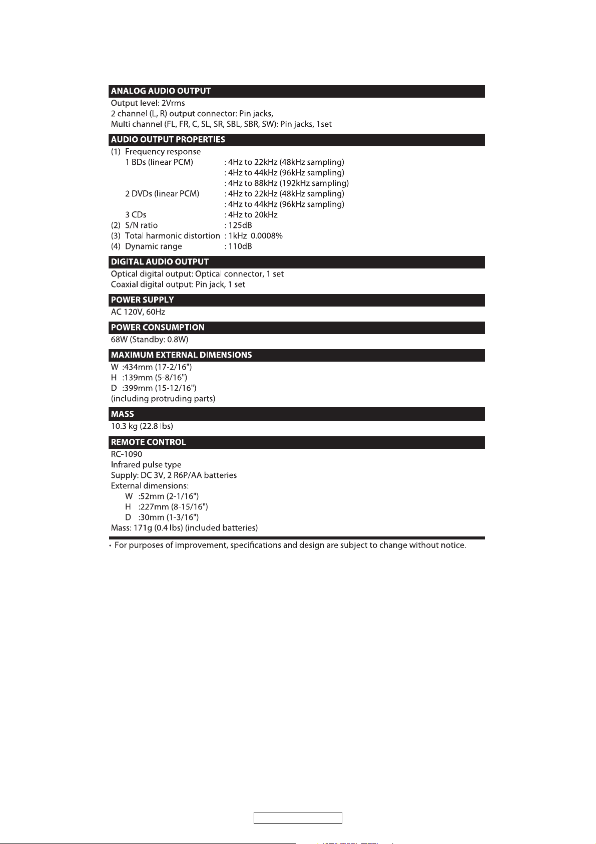
LASER BEAM SAFETY PRECAUTIONS
This BD player uses a pickup that emits a laser beam.
The laser beam is emitted from the location shown in the figure. When checking the laser diode, be sure to keep
your eyes at least 30 cm away from the pickup lens when the diode is turned on. Do not look directly at the laser
beam.
CAUTION: Use of controls and adjustments, or doing procedures other than those specified herein, may result in
hazardous radiation exposure.
Location: Top of BD mechanism.
Do not look directly at the laser beam coming
from the pickup or allow it to strike against your
skin.
Drive Mechanism Assembly
Laser Beam Radiation
Laser Pickup
Turntable
LASER RADIATION
WHEN OPEN. DO NOT
STARE INTO BEAM.
CAUTION
B1.0 Mechanism Assembly
d
7
DVD-3800BDCI
Page 8
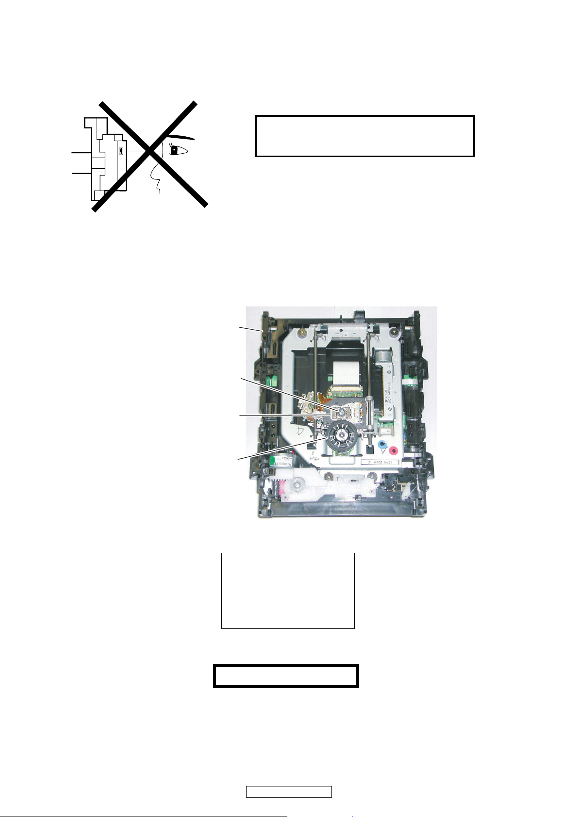
LASER BEAM SAFETY PRECAUTIONS
This BD player uses a pickup that emits a laser beam.
The laser beam is emitted from the location shown in the figure. When checking the laser diode, be sure to keep
your eyes at least 30 cm away from the pickup lens when the diode is turned on. Do not look directly at the laser
beam.
CAUTION: Use of controls and adjustments, or doing procedures other than those specified herein, may result in
hazardous radiation exposure.
Location: Inside Top of BD mechanism.
Do not look directly at the laser beam coming
from the pickup or allow it to strike against your
skin.
Drive Mechanism Assembly
Laser Beam Radiation
Laser Pickup
Turntable
d
B1.5 Mechanism Assembly
8
DVD-3800BDCI
Page 9
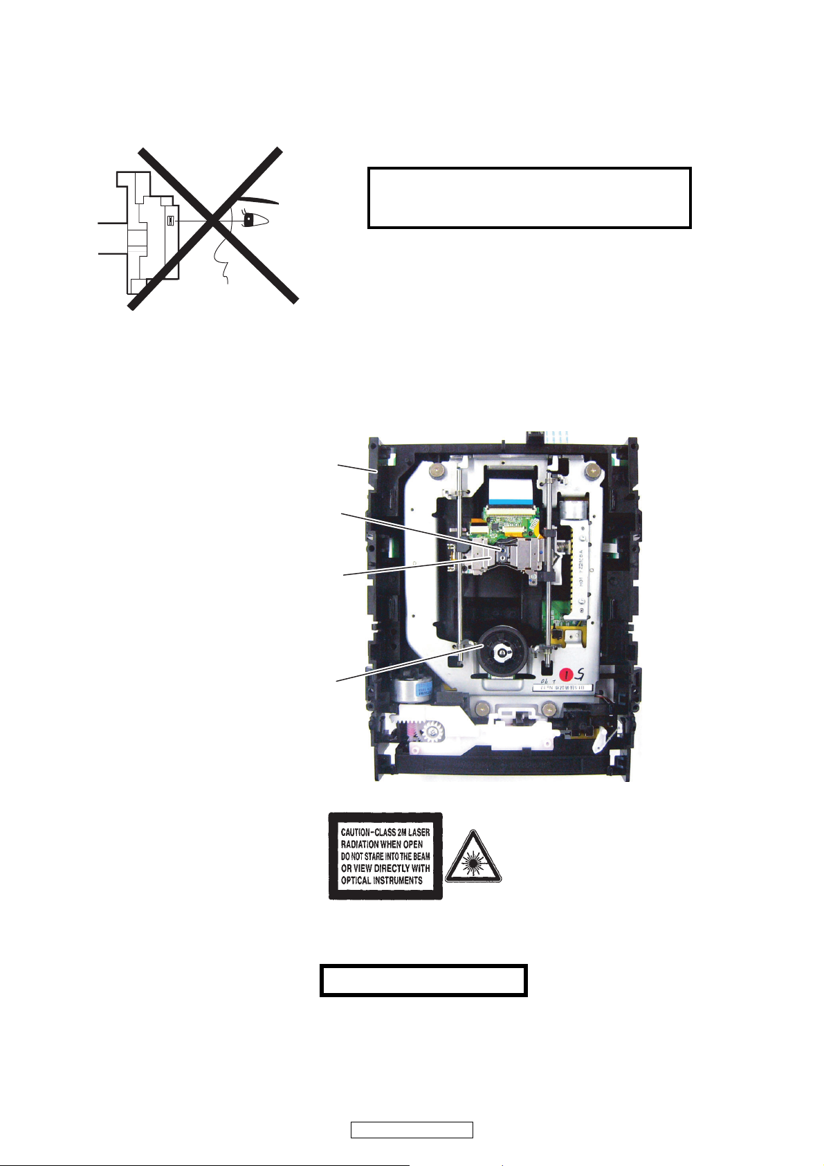
Safety Check after Servicing
Examine the area surrounding the repaired location for damage or deterioration. Observe that screws, parts, and
wires have been returned to their original positions. Afterwards, do the following tests and confirm the specified
values to verify compliance with safety standards.
1. Clearance Distance
When replacing primary circuit components, confirm
specified clearance distance (d) and (d’) between
soldered terminals, and between terminals and
surrounding metallic parts. (See Fig. 1)
Table 1: Ratings for selected area
Note: This table is unofficial and for reference only. Be
sure to confirm the precise values.
2. Leakage Current Test
Confirm the specified (or lower) leakage current
between B (earth ground, power cord plug prongs) and
externally exposed accessible parts (RF terminals,
antenna terminals, video and audio input and output
terminals, microphone jacks, earphone jacks, etc.) is
lower than or equal to the specified value in the table
below.
Measuring Method (Power ON):
Insert load Z between B (earth ground, power cord plug
prongs) and exposed accessible parts. Use an AC
voltmeter to measure across the terminals of load Z.
See Fig. 2 and the following table.
Table 2: Leakage current ratings for selected areas
Note: This table is unofficial and for reference only. Be sure to confirm the precise values.
AC Line Voltage Clearance Distance (d), (d’)
120 V ≥ 3.2 mm (0.126 inches)
AC Line Voltage Load Z Leakage Current (i) Earth Ground (B) to:
120 V
0.15 μF CAP. & 1.5 kΩ RES.
Connected in parallel
i ≤ 0.5 mA Peak Exposed accessible parts
Chassis or Secondary Conductor
Primary Circuit
Fig. 1
d' d
AC Voltmeter
(High Impedance)
Exposed Accessible Part
B
Earth Ground
Power Cord Plug Prongs
Z
Fig. 2
9
DVD-3800BDCI
Page 10
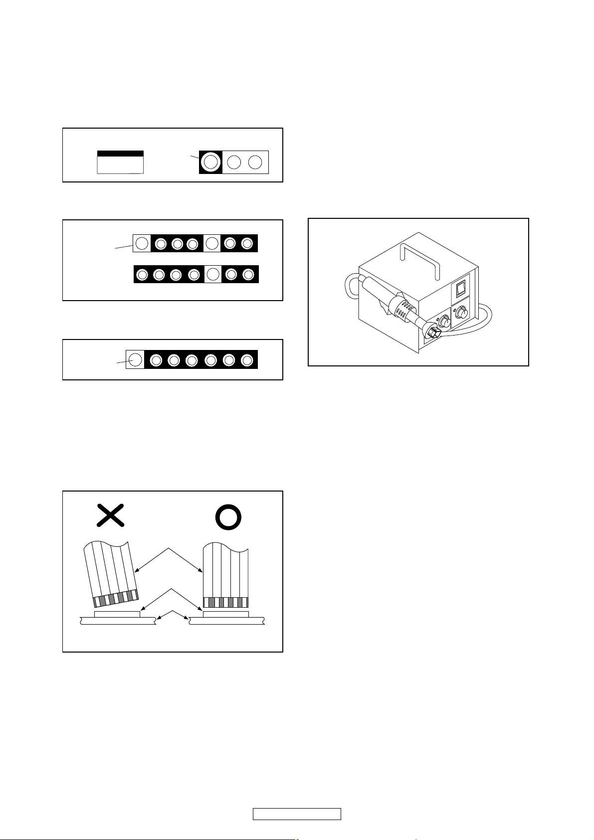
STANDARD NOTES FOR SERVICING
Circuit Board Indications
1. The output pin of the 3 pin Regulator ICs is
indicated as shown.
2. For other ICs, pin 1 and every fifth pin are
indicated as shown.
3. The 1st pin of every male connector is indicated as
shown.
Instructions for Connectors
1. When you connect or disconnect the FFC (Flexible
Foil Connector) cable, be sure to first disconnect
the AC cord.
2. FFC (Flexible Foil Connector) cable should be
inserted parallel into the connector, not at an
angle.
Pb (Lead) Free Solder
When soldering, be sure to use the Pb free solder.
How to Remove / Install Flat Pack-IC
1. Removal
With Hot-Air Flat Pack-IC Desoldering Machine:
1. Prepare the hot-air flat pack-IC desoldering
machine, then apply hot air to the Flat Pack-IC
(about 5 to 6 seconds). (Fig. S-1-1)
2. Remove the flat pack-IC with tweezers while
applying the hot air.
3. Bottom of the flat pack-IC is fixed with glue to the
CBA; when removing entire flat pack-IC, first apply
soldering iron to center of the flat pack-IC and heat
up. Then remove (glue will be melted). (Fig. S-1-6)
4. Release the flat pack-IC from the CBA using
tweezers. (Fig. S-1-6)
CAUTION:
1. The Flat Pack-IC shape may differ by models. Use
an appropriate hot-air flat pack-IC desoldering
machine, whose shape matches that of the Flat
Pack-IC.
2. Do not supply hot air to the chip parts around the
flat pack-IC for over 6 seconds because damage
to the chip parts may occur. Put masking tape
around the flat pack-IC to protect other parts from
damage. (Fig. S-1-2)
Top View
Out
In
Bottom View
Input
5
10
Pin 1
Pin 1
FFC Cable
Connector
CBA
* Be careful to avoid a short circuit.
Fig. S-1-1
10
DVD-3800BDCI
Page 11
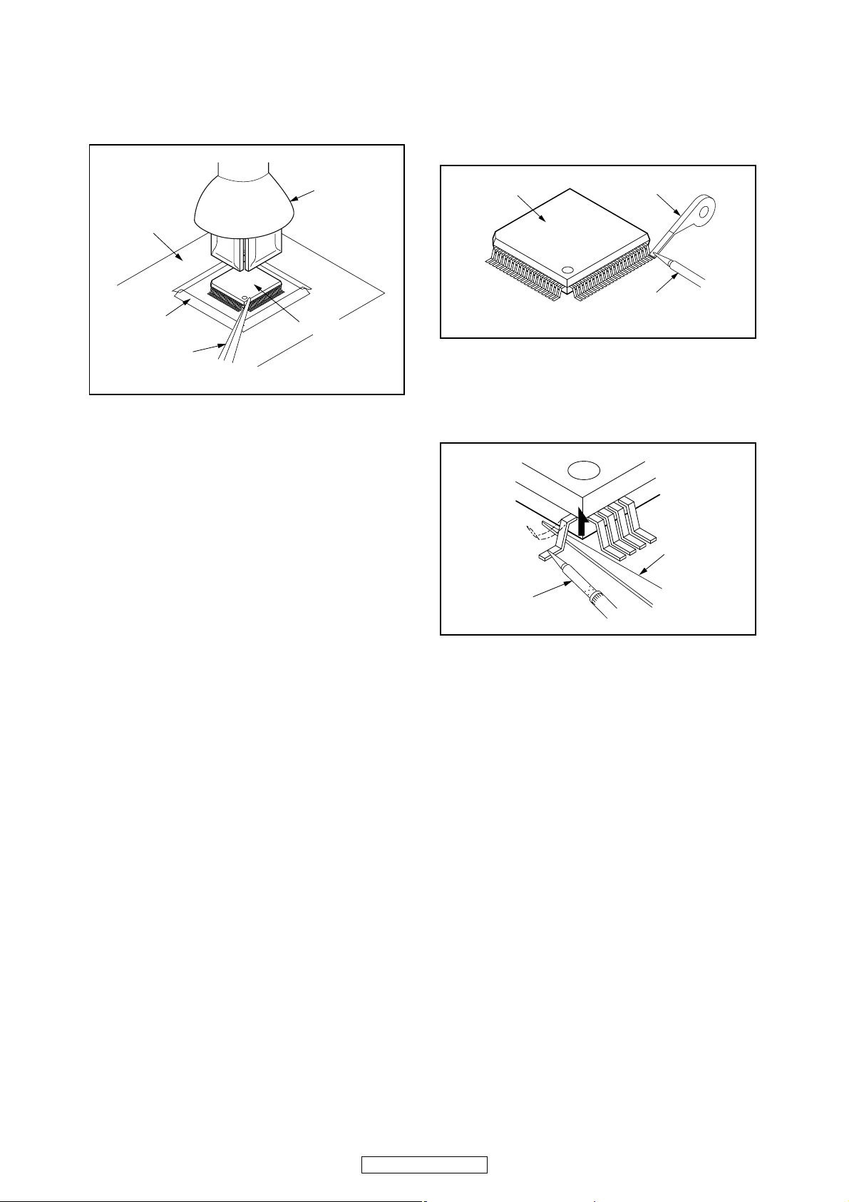
3. The flat pack-IC on the CBA is affixed with glue, so
be careful not to break or damage the foil of each
pin or the solder lands under the IC when
removing it.
With Soldering Iron:
1. Using desoldering braid, remove the solder from
all pins of the flat pack-IC. When you use solder
flux which is applied to all pins of the flat pack-IC,
you can remove it easily. (Fig. S-1-3)
2. Lift each lead of the flat pack-IC upward one by
one, using a sharp pin or wire to which solder will
not adhere (iron wire). When heating the pins, use
a fine tip soldering iron or a hot air desoldering
machine. (Fig. S-1-4)
3. Bottom of the flat pack-IC is fixed with glue to the
CBA; when removing entire flat pack-IC, first apply
soldering iron to center of the flat pack-IC and heat
up. Then remove (glue will be melted). (Fig. S-1-6)
4. Release the flat pack-IC from the CBA using
tweezers. (Fig. S-1-6)
Hot-air
Flat Pack-IC
Desoldering
Machine
CBA
Flat Pack-IC
Tweezers
Masking
Tape
Fig. S-1-2
Flat Pack-IC
Desoldering Braid
Soldering Iron
Fig. S-1-3
Fine Tip
Soldering Iron
Sharp
Pin
Fig. S-1-4
11
DVD-3800BDCI
Page 12
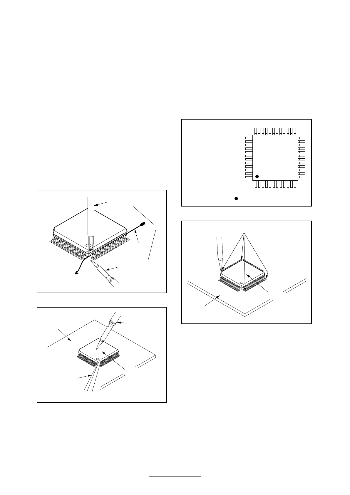
With Iron Wire:
1. Using desoldering braid, remove the solder from
all pins of the flat pack-IC. When you use solder
flux which is applied to all pins of the flat pack-IC,
you can remove it easily. (Fig. S-1-3)
2. Affix the wire to a workbench or solid mounting
point, as shown in Fig. S-1-5.
3. While heating the pins using a fine tip soldering
iron or hot air blower, pull up the wire as the solder
melts so as to lift the IC leads from the CBA
contact pads as shown in Fig. S-1-5.
4. Bottom of the flat pack-IC is fixed with glue to the
CBA; when removing entire flat pack-IC, first apply
soldering iron to center of the flat pack-IC and heat
up. Then remove (glue will be melted). (Fig. S-1-6)
5. Release the flat pack-IC from the CBA using
tweezers. (Fig. S-1-6)
Note: When using a soldering iron, care must be
taken to ensure that the flat pack-IC is not
being held by glue. When the flat pack-IC is
removed from the CBA, handle it gently
because it may be damaged if force is applied.
2. Installation
1. Using desoldering braid, remove the solder from
the foil of each pin of the flat pack-IC on the CBA
so you can install a replacement flat pack-IC more
easily.
2. The “●” mark on the flat pack-IC indicates pin 1.
(See Fig. S-1-7.) Be sure this mark matches the 1
on the PCB when positioning for installation. Then
presolder the four corners of the flat pack-IC. (See
Fig. S-1-8.)
3. Solder all pins of the flat pack-IC. Be sure that
none of the pins have solder bridges.
To Solid
Mounting Point
Soldering Iron
Iron Wire
or
Hot Air Blower
Fig. S-1-5
Fine Tip
Soldering Iron
CBA
Flat Pack-IC
Tweezers
Fig. S-1-6
Example :
Pin 1 of the Flat Pack-IC
is indicated by a " " mark.
Fig. S-1-7
Presolder
CBA
Flat Pack-IC
Fig. S-1-8
12
DVD-3800BDCI
Page 13
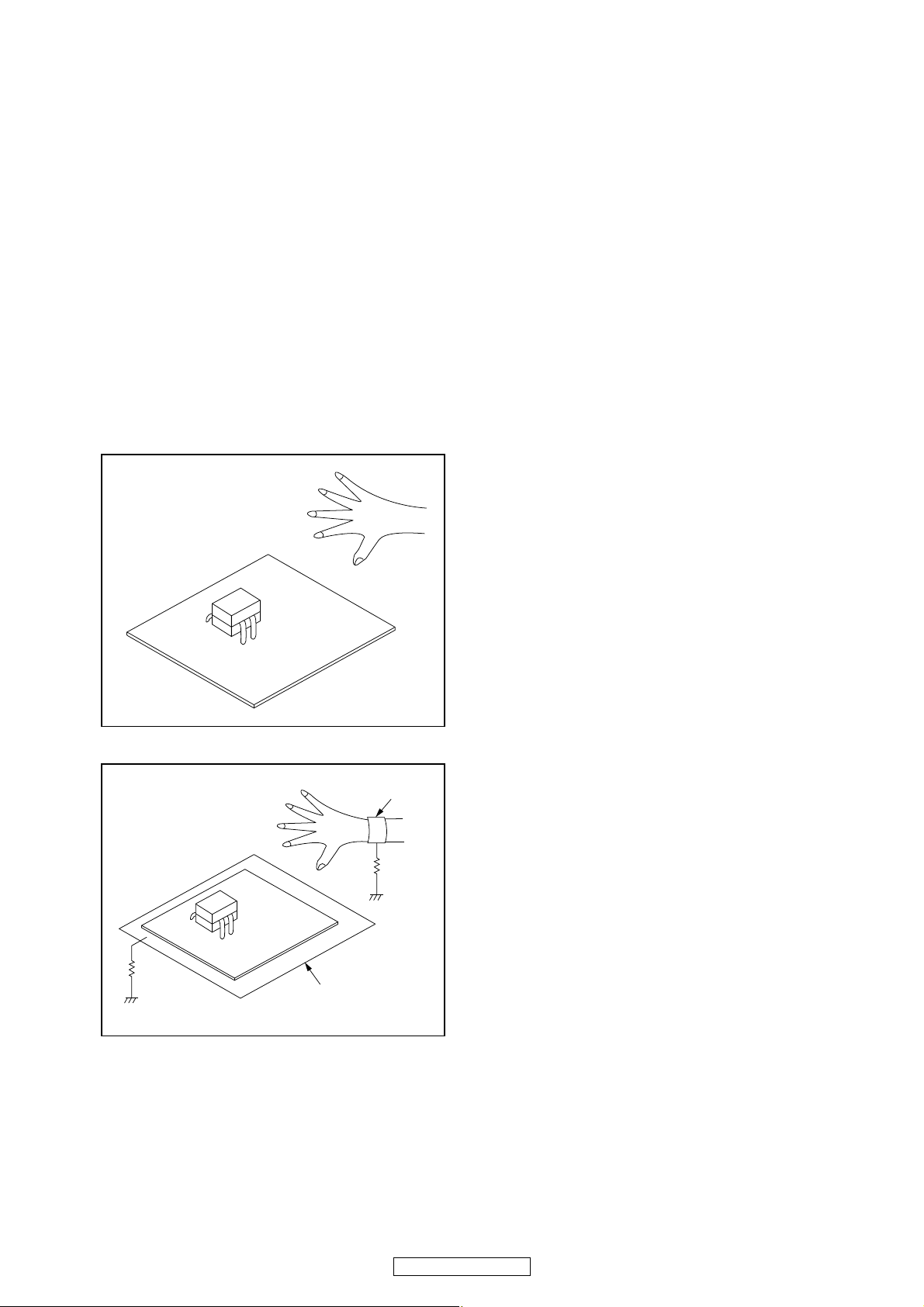
Instructions for Handling Semiconductors
Electrostatic breakdown of the semi-conductors may
occur due to a potential difference caused by
electrostatic charge during unpacking or repair work.
1. Ground for Human Body
Be sure to wear a grounding band (1 MΩ) that is
properly grounded to remove any static electricity that
may be charged on the body.
2. Ground for Workbench
Be sure to place a conductive sheet or copper plate
with proper grounding (1 MΩ) on the workbench or
other surface, where the semi-conductors are to be
placed. Because the static electricity charge on
clothing will not escape through the body grounding
band, be careful to avoid contacting semi-conductors
with your clothing.
<Incorrect>
CBA
Grounding Band
Conductive Sheet or
Copper Plate
1MΩ
1MΩ
<Correct>
CBA
13
DVD-3800BDCI
Page 14
CABINET DISASSEMBLY INSTRUCTIONS
1. Disassembly Flowchart
This flowchart indicates the disassembly steps to gain
access to item(s) to be serviced. When reassembling,
follow the steps in reverse order. Bend, route, and
dress the cables as they were originally.
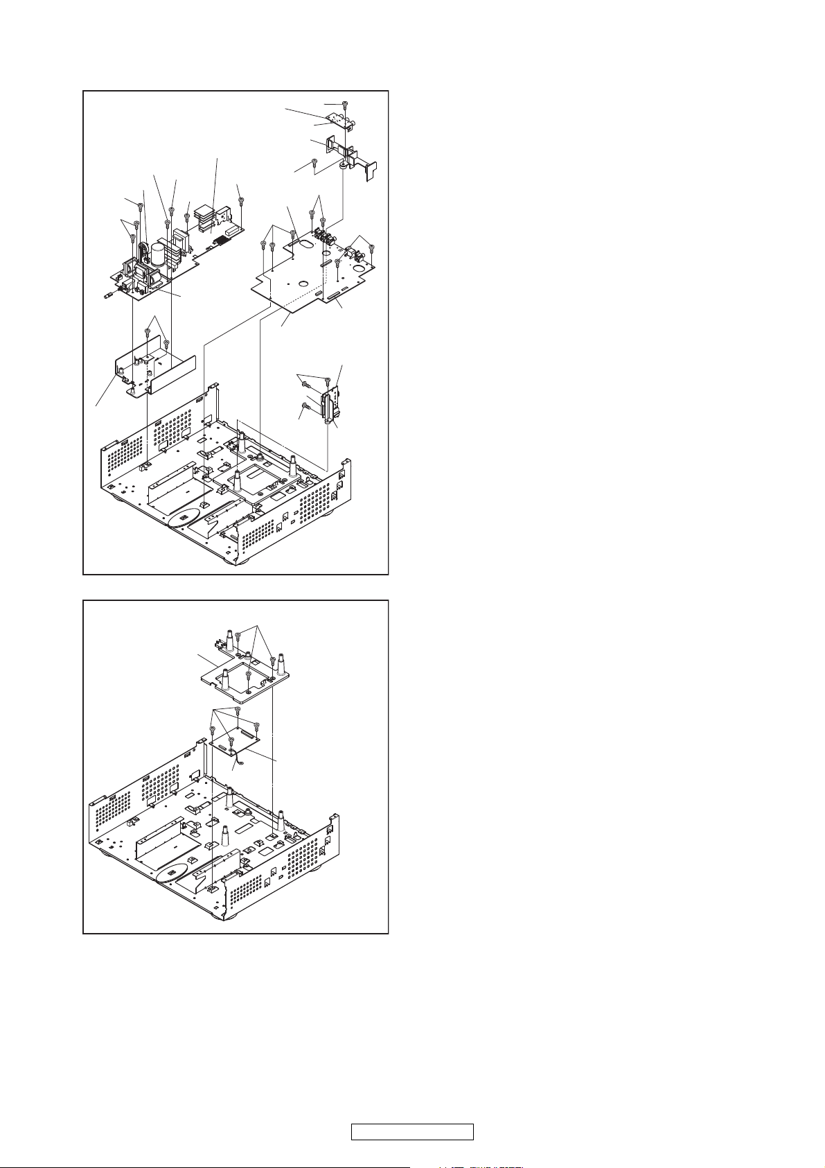
2. Disassembly of Main parts
When replacing the main parts, see the following procedures. For more details, refer to Fig. D1~D10.
*About *[9](S-14), remove only (S-14) of Rear Panel.
3. Disassembly Method
Part Steps
[10] BE Main CBA Unit [1] → [2] → *[9](S-14) → [10]
[11] Scaler CBA Unit
[1]→[2]→ [3]→ *[9](S-14)→ [10]
→ [11]
[12] D-Audio CBA Unit [1] → [2] → [9] → [12]
[13] F-Audio CBA Unit [1] → [2] → [9] → [12] → [13]
[14] S-Audio CBA Unit [1]→[2]→[9]→ [12]→[13]→[14]
[15] ADSP CBA Unit
[1]→[2]→[9]→[10]→[11]→ [12]
→ [13] → [14] → [15]
[16]
FE Main CBA & BD
Mechanism
Assembly
[1]→[2]→ [3]→ *[9](S-14)→ [10]
→ [16]
[17] Fan Holder
[1] → [2] → *[9](S-14) → [10] →
[11] → [17]
[1] Top Cover
[6] Power Switch CBA
[7] SD CBA
[3] Tray Panel
[4] Front Assembly
[8] Front Bracket
[2] Top Panel
[19] RS232C CBA
[20] Jack CBA
[23] AV CBA
[25] Pedestal
[21] Power
Supply CBA
[22] Sub Power
CBA
[24] Sub
Microcontroller
CBA
[9] Rear Panel
[10] BE Main CBA Unit
[11] Scaler CBA Unit
[12] D-Audio CBA
[13] F-Audio CBA
Analog Audio CBA Unit
[14] S-Audio CBA
[15] ADSP CBA Unit
[16] FE Main CBA & BD Mechanism Assembly
[18] Fan Motor
[5] Front CBA
[17] Fan Holder
[18] Fan Motor
[1] → [2] → *[9](S-14) → [10] →
[11] → [17] → [18]
[19] RS232C CBA [1]→[2]→ [9]→[10]→[11]→[19]
[20] Jack CBA
[1]→[2]→ [9]→[10]→[11]→[19]
→ [20]
[21] Power Supply CBA
[1] → [2] → *[9](S-14) → [10] →
[11] → [17] → [21]
[22] Sub Power CBA [1] → [2] → [3] → [4] → [8] → [22]
[23] AV CBA
[1]→ [2]→ [3]→ [9]→ [10]→ [11]
→ [12] → [13] → [14] → [23]
[24]
Sub Microcontroller
CBA
[1] → [2] → [12] → [13] → [14] →
[24]
ID/
Loc.
No.
Part
Removal
Fig.
No.
Remove/*Unhook/
Unlock/Release/
Unplug/Desolder
Note
[1] Top Cover D1 9(S-1), 2(S-2) --[2] Top Panel D2 10(S-3) --[3] Tray Panel D3 *2(L-1) 1
[4]
Front
Assembly
D3
2(S-4), 2(S-5), (S-5a),
*3(L-2), *CN2001,
*CN4002
1
[5] Front CBA D4 7(S-6) ---
[6]
Power
Switch CBA
D4 2(S-7), Desolder ---
[7] SD CBA D4
2(S-8), SD PCB
Holder
---
[8]
Front
Bracket
D5 2(S-9) ---
[9] Rear Panel D5
2(S-10), 2(S-11),
2(S-12), 18(S-13),
4(S-14), 3(S-15),
2(S-16) *CN1001
2
[10]
BE Main
CBA Unit
D6
4(S-17), *CN6401,
*CN7001, *CN7401,
*CX813
2
[11]
Scaler CBA
Unit
D6
4(S-18), 3(S-19),
3(S-20), *CX874,
*CX875, *CY080,
BE Scaler Holder, BE
Scaler Sub Holder
---
[12]
D-Audio
CBA
D7 2(S-21), *CX877 ---
14
DVD-3800BDCI
Page 15
Note:
(1) Identification (location) No. of parts in the figures
(2) Name of the part
(3) Figure Number for reference
(4) Identification of parts to be removed, unhooked,
unlocked, released, unplugged, unclamped, or
desoldered.
P = Spring, L = Locking Tab, S = Screw,
CN = Connector
* = Unhook, Unlock, Release, Unplug, or Desolder
e.g. 2(S-2) = two Screws (S-2),
2(L-2) = two Locking Tabs (L-2)
(5) Refer to “Reference Notes.”
About tightening screws
When tightening screws, tighten them with the
following torque.
Reference Notes
1. CAUTION 1: Locking Tabs (L-1) and (L-2) are
fragile. Be careful not to break them.
1) Release three Locking Tabs (L-2).
2) Disconnect connectors CN2001, CN4002, then
remove the Front Assembly.
2. CAUTION 2: When installing the BE Main CBA
Unit with a screw, hold and press the BE Main
CBA Unit to align the HDMI connector with the
connector’s hole for HDMI on the Rear Panel.
[13]
F-Audio
CBA
D7
3(S-22), *CN061,
*CN10, *CX201,
*CY281
---
[14]
S-Audio
CBA
D7 3(S-23) ---
[15]
ADSP CBA
Unit
D7
2(S-24), (S-25),
4(S-26), 2(S-27),
*CX876, DSP PCB
Holder, Audio PCB
Holder
---
[16]
FE Main
CBA & BD
Mechanism
Assembly
D8 4(S-28), *CN2601 ---
[17] Fan Holder D8 2(S-29), *CN2500 --[18] Fan Motor D8 2(S-30) ---
[19]
RS232C
CBA
D9
3(S-31), *CN2551,
RS232C Holder
---
[20] Jack CBA D9
(S-32), (S-33),
*CN2730, BNC PCB
Holder
---
[21]
Power
Supply
CBA
D9
2(S-34), 2(S-35),
*CN101, *CN2501
---
[22]
Sub Power
CBA
D9
3(S-36), 2(S-37),
Power PCB Holder
---
[23] AV CBA D9 7(S-38), *CN2503 ---
[24]
Sub
Microcontro
ller CBA
D10 4(S-39) ---
[25] Pedestal D10 3(S-40) ---
↓
(1)
↓
(2)
↓
(3)
↓
(4)
↓
(5)
ID/
Loc.
No.
Part
Removal
Fig.
No.
Remove/*Unhook/
Unlock/Release/
Unplug/Desolder
Note
Torque
0.45 ± 0.05 N·m
(S-2)
(S-2)
(S-1)
(S-1)
(S-1)
(S-1)
(S-1)
Fig. D1
[1] Top Cover
15
DVD-3800BDCI
Page 16
(S-3)
(S-3)
(S-3)
(S-3)
[2] Top Panel
Fig. D2
[3] Tray Panel
[4] Front Assembly
(S-5)
(S-4)
(S-5a)
(S-5)
(S-4)
CN4002
(L-2)
(L-1)
(L-1)
CN2001
Fig. D3
(S-6)
(S-6)
(S-7)
(S-8)
Fig. D4
[6] Power Switch CBA
[7] SD CBA
[5] Front CBA
SD PCB
Holder
Desolder
Lead with
blue stripe
CN1001
(S-15)
(S-10)
(S-10)
(S-15)
(S-15)
(S-12)
(S-14)
(S-14)
*(S-14)
(S-11)
(S-13)
(S-13)
(S-13)
(S-13)
(S-13)
(S-16)
Fig. D5
[9] Rear Panel
(S-9)
(S-9)
[8] Front Bracket
16
DVD-3800BDCI
Page 17
(S-17)
(S-17)
(S-18)
(S-18)
(S-19)
(S-20)
(S-19)
CN6401
BE Scaler
Holder
BE Scaler
Sub Holder
CN7001
CX813
CY080
CN817
CN7401
[11] Scaler
CBA Unit
[10] BE Main
CBA Unit
CX874
CX875
Fig. D6
(S-21)
(S-22)
(S-22)
(S-22)
(S-23)
(S-27)
(S-27)
(S-26)
(S-24)
(S-25)
(S-26)
CX876
Audio PCB Holder
DSP PCB Holder
[12] D-Audio CBA
[13] F-Audio CBA
[14] S-Audio CBA
[15] ADSP CBA
Unit
CY281
CX201
CX877
CN061
CN10
Fig. D7
(S-28)
(S-28)
(S-28)
(S-29)
(S-29)
(S-30)
CN2500
CN2601
[16] FE Main CBA &
BD Mechanism Assembly
[17] Fan Holder
[18] Fan Motor
Fig. D8
17
DVD-3800BDCI
Page 18
(S-31)
(S-31)
(S-34)
(S-34)
(S-35)
(S-35)
(S-36)
(S-36)
Power PCB
Holder
RS232C
Holder
BNC PCB Holder
(S-38)
(S-38)
(S-32)
CN2730
(S-33)
(S-38)
(S-37)
CN101
CN2551
CN2501
CN2503
Fig. D9
[19] RS232C CBA
[21] Power Supply CBA
[20] Jack CBA
[22] Sub
Power CBA
[23] AV CBA
(S-39)
Wire
(S-40)
Fig. D10
[24] Sub
Microcontroller
CBA
[25] Pedestal
18
DVD-3800BDCI
Page 19
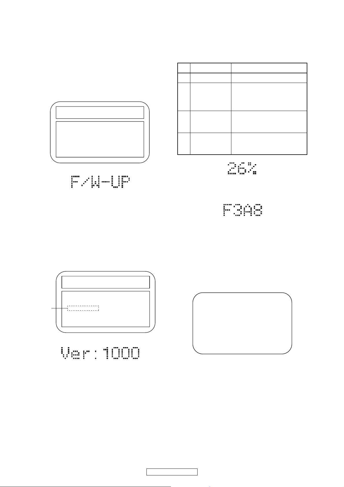
4. How to Eject Manually
1. Remove the Top Cover and the Top Panel.
2. Insert a screwdriver, etc. into the Hole A straightly so that the Portion A is pushed.
3. Pull the tray out manually and remove a disc.
Portion A
Hole A
Screwdriver,
hexagon wrench
19
DVD-3800BDCI
Page 20

HOW TO INITIALIZE THE BLU-RAY DISC PLAYER
To put the program back at the factory-default,
initialize the BD player as the following procedure.
1. Turn the power on.
2. Remove the disc on the tray and close the tray.
3. Press [1], [2], [3], [4], and [DISPLAY] buttons on
the remote control unit in that order.
Fig. a appears on the screen.
4. Press [STOP] button on the remote control unit.
Fig. b appears on the screen and Fig. c appears
on the VFD.
5. To exit this mode, press [POWER OFF] button.
Fig. a
"
*******
" differ depending on the models.
Model Name : *******
Version
: *.***
Region
: *-*
ADSP1/2 Ver. : ****/****
PLD Ver. : *
FPGA Ver. : **
I/P Scaler Ver. : ******
EXIT: POWEREEPROM CLEAR : STOP
Fig. b
"
*******
" differ depending on the models.
Model Name : *******
Version
: *.***
Region
: *-*
ADSP1/2 Ver. : ****/****
PLD Ver. : *
FPGA Ver. : **
I/P Scaler Ver. : ******
EXIT: POWEREEPROM CLEAR : STOP
EEPROM CLEAR : OK
Fig. c
d
20
DVD-3800BDCI
Page 21
FIRMWARE RENEWAL MODE
1. Turn the power on and remove the disc on the tray.
2. To put the BD player into version up mode, press
[9], [8], [7], [6], and [POP UP MENU/MENU]
buttons on the remote control unit in that order.
The tray will open automatically.
Fig. a appears on the screen and Fig. b appears
on the VFD.
The BD player can also enter the version up mode
with the tray open. In this case, Fig. a will be
shown on the screen while the tray is open.
3. Load the disc for version up.
4. The BD player enters the F/W version up mode
automatically. Fig. c appears on the screen and
Fig. d appears on the VFD. If you enter the F/W for
different models, “Disc Error” will appear on the
screen, then the tray will open automatically.
The appearance shown in (*1) of Fig. c is
described as follows:
5. After programming is finished, the checksum on
the VFD (Fig. f).
At this time, no button is available.
6. Unplug the AC cord from the AC outlet. Then plug
it again.
7. Turn the power on.
8. Press [1], [2], [3], [4], and [DISPLAY] buttons on
the remote control unit in that order.
Fig. g appears on the screen.
F/W VERSION UP MODE Model No : ******* Ver. : *.***
ADSP 1/2 Ver. : ***/***
Please insert a DISC
for F/W Version Up.
"
*******
" differs depending on the models.
Fig. a Version Up Mode Screen
Fig. b VFD in Version Up Mode
1. ALL
Now Loading...
Ver. : *.** ************A*.bin
(*1)
F/W VERSION UP MODE Model No : ******* Ver. : *.***
ADSP 1/2 Ver. : ***/***
"
*******
" differs depending on the models.
Fig. c Programming Mode Screen (Example
)
Fig. d VFD in Programming Mode (Example)
No. Appearance State
1 Now Loading... Loading the disc
2 Reading...
Sending files into the
memory.
After reading, automatically
the tray opens.
3
Remove the
disc
Reading has finished.
Remove the disc and close
the tray.
4 See FL display
Writing new version data,
the progress will be displayed
as shown in Fig. e.
Fig. e VFD in Version Up Mode
Fig. f VFD upon Finishing the Programming Mode (Example)
Fig. g
"
*******
" differ depending on the models.
Model Name : *******
Version
: *.***
Region
: *-*
ADSP1/2 Ver. : ****/****
PLD Ver. : *
FPGA Ver. : **
I/P Scaler Ver. : ******
EXIT: POWEREEPROM CLEAR : STOP
d
21
DVD-3800BDCI
Page 22

9. Press [STOP] button on the remote control unit.
Fig. h appears on the screen and Fig. i appears on
the VFD.
10. To exit this mode, press [POWER OFF] button.
How to Verify the Firmware Version
1. Turn the power on.
2. Remove the disc on the tray and close the tray.
3. Press [1], [2], [3], [4], and [DISPLAY] buttons on
the remote control unit in that order.
Fig. j appears on the screen.
4. To exit this mode, press [POWER OFF] button.
Fig. h
"
*******
" differ depending on the models.
Model Name : *******
Version
: *.***
Region
: *-*
ADSP1/2 Ver. : ****/****
PLD Ver. : *
FPGA Ver. : **
I/P Scaler Ver. : ******
EXIT: POWEREEPROM CLEAR : STOP
EEPROM CLEAR : OK
Fig. i
Fig.
j
"
*******
" differ depending on the models.
Model Name : *******
Version
: *.***
Region
: *-*
ADSP1/2 Ver. : ****/****
PLD Ver. : *
FPGA Ver. : **
I/P Scaler Ver. : ******
EXIT: POWEREEPROM CLEAR : STOP
d
b The region setting can be changed up to five
times (including factory preset).
If you exceed the region change limit, DVD
playback images will be affected by noise.
Version Up Mode
s
Realta update (GU-3867: DIGITAL VIDEO UNIT)
1. The RS-232C terminal of DVD3800BD and PC are
connected with RS-232C cable.
2. The 6-2 (Version Up mode with RS-232C) is
selected from the service mode (Refer to page
22).
3. The Realta version up software is started with PC,
and the firmware is rewritten. (Refer to the Realta
version up manual )
22
DVD-3800BDCI
Page 23
SERVICE MODE
Service Mode
Note: If some test are performed continuously, any error will occur.
1st level 2nd level 3rd level Description
1 Mecha test
1 Tray Aging Aging of tray open/close
2 TOC Read TOC reading
3 Heat Run
Tray close -> TT1 playback -> TT10
playback -> Tray open -> Tray
close
2 VFD/LED Test
1 All On Turning on all VFD
2 All Off Turning off all VFD
3 Error Rate
Displaying Error rate, Jitter
during playback
4 LD Test
1LD Power
1 Off Turning off LD
2 BD Turning on BD LD
3 DVD Turning on DVD LD
4 CD Turning on CD LD
2 Operating Time
1 BD Displaying BD LD Operation Time
2 DVD Displaying DVD LD Operation Time
3 CD Displaying CD LD Operation Time
4STOP
Clear LD Operation Total Time
※
When the mechanism is replaced, LD Operation Total
Time is cleared.
5 Channel Level
1 TEST TONE
1
Center/
Subwoofer/Front
LR
2
Surround LR/
Surround Back LR
2 Front Lch
3 Center
4 Front Rch
5 Surround Rch
6
Surround Back
Rch
7
Surround Back
Lch
8 Surround Lch
9 Sub woofer
6 RS-232C
1 Parity Setting
1 Even Setting even parity
2 Non Setting non parity
2 Version Up Mode
Realta Version up with connecting
RS-232C
7 SD Card Test
8 Default Setting Default setting
s
23
DVD-3800BDCI
Page 24
Entering Service Mode
In power on condition, no discs and tray close, it will be entered into service mode by the following operation using
the remote controller. However, it will not be entered when Media Select Item is SD Memory.
Service Mode by using remote controller
Press the following buttons on the remote controller in power on condition, no discs and tray close;
[2]->[5]->[8]->[0]->[CLEAR]
Release from Service Mode
Press the [POWER OFF] button to turn off power.
Screen saver/Auto Power Off in Service Mode
These functions are not performed in Service Mode.
After entering, Fig. j appears on the screen and Fig. k appears on the VFD.
Available button in service mode
Note:Press the number key to select items. Or, press the cursor button (up/down) to select items and press
[ENTER] button.
Button condition
ENTER Enter the next level
POWER Turn the power off (when the service mode is completed)
1~8 Enter the selected item (next level)
OTHER Not available
INDICATION DESCRIPTION REMARK
Model Name Model Name E5E***D, etc.
Region BD region - DVD region A-1, etc.
Rel. Ver. Release version
Service Mode
1. Mecha Test
2. VFD/LED Test
3: Error Rate
4: LD Test
5: RS-232C
6: Channel Level
7: SD Card Test
8: Default Setting
Model: :E5E**UD Region :A-1
Release Ver. :*.***
ADSP1/2 Ver.: ****/**** PLD Ver. :*
FPGA Ver.:** I/P Scaler Ver.:*****
Fig. j Service Mode (Main menu)
* Firmware Version differs depending on the
models, and this indication is one example.
Fig. k Service Mode
24
DVD-3800BDCI
Page 25

TRAY LOCK MODE
Tray Lock Mode prevents the tray opening or closing to
prevent disc theft in demo mode.
Enter this mode using the following procedure.
1. Confirm that the TV Monitor is connected.
2. With playback stopped, press [SETUP], [TOP
MENU], [3], [AUDIO], [0] and [SETUP] buttons on
the remote control unit in that order. "Trade On" will
appear in the upper right corner on the screen, and
on VFD for 2 seconds.
3. To exit this mode, press [SETUP], [TOP MENU],
[3], [AUDIO], [0] and [SETUP] buttons on the
remote control unit in that order. "Trade Off" will
appear in the upper right corner on the screen, and
on VFD for 2 seconds.
Fig.a VFD
Fig.b VFD
25
DVD-3800BDCI
Page 26

REMOTE LOCK MODE
SETTING MENU:
Remote Lock Off Mode:
This mode receives an input signal from the remote
control unit or from the Remote In-Jack on the rear
panel.
Remote Lock On Mode:
This mode dose not receive an input signal from
the remote control unit or from the Remote In-Jack
on the rear panel.
Perform the setting using the following procedure.
1. Press [ON/STANDBY] and [STOP] buttons on the
front panel simultaneously for over 3 seconds to set
"Remote Lock Mode" and display mode.
2. Press [STILL/PAUSE] button on the remote control
unit to set to "On" or "Off". When "Remote Lock
On", "Remote Lock On" will appear in the upper
right corner on the screen and appears on the VFD.
When "Remote Lock Off", "Remote Lock Off" will
appear in the upper right corner on the screen and
appears on the VFD.
a. If [STILL/PAUSE] button is not pressed for 5
seconds or any other button is pressed within 5
seconds, the unit will be released from
"Remote Lock Mode".
b. When initializing, set the Remote Lock Mode
"off".
Fig.a VFD
Fig.b VFD
26
DVD-3800BDCI
Page 27
TROUBLESHOOTING
FLOW CHART NO.2
The fuse blows out.
After servicing, replace the fuse.
Check the presence that the primary component
is leaking or shorted and service it if defective.
Check the presence that the rectifying diode or
circuit is shorted in each rectifying circuit of
secondary side, and service it if defective.
FLOW CHART NO.3
When the output voltage fluctuates.
Ye s
No
FLOW CHART NO.4
When buzz sound can be heard in the vicinity of power circuit.
Check if there is any short-circuit on the rectifying diode and the circuit in each rectifying circuit of the secondary
side
, and service it if defective.
(D1112, D1113, D1114, D1115, D1116, D1118, D1120, D1121,D1122, D1124, D1146,
IC1105, IC1106, IC2600, IC2601, Q2600, Q2606, Q2608, Q2610, Q2611)
Does the photo coupler circuit on the secondary
side operate normally?
Check D1107, IC1101, IC1103 and their periphery,
and service it if defective.
Check D1117, D1129, IC1103 and their periphery,
and service it if defective.
FLOW CHART NO.5
-FL is not outputted.
Is -30V voltage supplied to the emitter of Q2503?
Check D1118, D1130, C1126 and periphery circuit,
and service it if defective.
Check Q2503 and their periphery, and service it if
defective.
Check FL-SW line and service
it if defective.
Is the "L" signal outputted to the collector of
Q2507?
Ye s
Ye s
Ye s
Ye s
No
No
No
No
No
FLOW CHART NO.1
The power cannot be turned on.
Is the fuse normal?
Is normal state restored when once unplugged
power cord is plugged again after several seconds?
Is the AL+5V line voltage normal?
See FLOW CHART No.2 <The fuse blows out.>
Check if there is any leak or short-circuiting on the
primary circuit component, and service it if defective.
(D1101, D1102, D1103, D1104, D1109, D1110,
IC1101, Q1103, T1101, C1110, R1117)
Check each rectifying circuit of the secondary circuit
and service it if defective.
Ye s
Ye s
Ye s
No
No
No
Is 3.3V voltage supplied to the emitter of Q2504?
Ye s
Is 3.3V voltage outputted to collector of Q2504?
Is the "H" signal inputted to the base of Q2507?
Replace Q2507.
Replace Q2504.
Check EV+3.3V line and service it if defective.
27
DVD-3800BDCI
Page 28
FLOW CHART NO.6
Is 5V voltage inputted to the emitter of Q2610?
Replace Q2611.
Ye s
No
Is 11V voltage inputted to the base of Q2611? Is 13.5V voltage inputted to the base of Q2605?
Check D1122, D1128, C1124, L1105
and
their periphery, and service it if defective.
No
FLOW CHART NO.7
FLOW CHART NO.8
P-ON+10.5V is not outputted.
Is 13.5V voltage inputted to the collector of Q2611?
Ye s Ye s No
Ye s
Check D1115, C1119
and their periphery circuit,
and service it if defective.
Check Q2605, D2601,
and their periphery, and
service it if defective.
Check Q2604,
and
PWSW3 line, and
service it if defective.
Is 2.5V voltage supplied to Pin(1) of IC2601?
Ye s
No
FLOW CHART NO.9
P-ON+1.2V is not outputted.
Replace IC2601.
Is the voltage of base on Q2610 lower than the
voltage of emitter on Q2610 when turning the power on?
Replace Q2610.
Check Q2607 and PWSW3 line and service it if
defective.
Ye s
No
Check D1112, D1113, D1114, D1129, C1125, C1132
and their periphery, and service it if defective.
Is 5V voltage inputted to the emitter of Q2606?
Ye s
No
Is the voltage of base on Q2606 lower than the
voltage of emitter on Q2606 when turning the power on?
Replace Q2606.
Check Q2607 and PWSW3 line and service it if
defective.
Ye s
No
No
Check D1112, D1113, D1114, D1129, C1125, C1132
and their periphery, and service it if defective.
P-ON+5V (2) is not outputted.
FLOW CHART NO.10
P-ON+3.3V is not outputted.
Is 5V voltage supplied to Pin(1) of IC2600?
ls "L" signal outputted to the collector of Q2603?
Check D1112, D1113, D1114, D1129, C1125, C1132 and
their periphery circuit, and service it if defective.
Check IC2600, D2600 and their periphery circuit,
and service it if defective.
Ye s
Ye s
No
Check Q2603 and PWSW3 line and service it if
defective.
No
P-ON+5V (1) is not outputted.
DVD-3800BDCI
28
Page 29
EV+3.3V(2) is not outputted.
(AL+5V is output normally.)
FLOW CHART NO.11
Is 14V voltage inputted to the emitter of Q2609?
Replace Q2613.
Ye s
No
Is 2.6V voltage inputted to the base of Q2613?
Check D1145, R1128, R1129, R1130
and
their periphery, and service it if defective.
No
FLOW CHART NO.12
Check Q2612
and A33-PW-CONT line,
and service it if defective.
FLOW CHART NO.13
Is 3.3V voltage inputted to the emitter of Q2613?
Ye s
Ye s
Is the voltage of base on Q2609 lower than the
voltage of emitter on Q2609 when turning the power on?
Replace Q2609.
Check Q2604 and PWSW3 line and service it if
defective.
Ye s
No
Check D1121, D1127, C1123, L1104 and their
periphery, and service it if defective.
Is -12V voltage inputted to the emitter of Q2600?
Ye s
No
No
Is 5V voltage inputted to the emitter of Q2602?
Replace Q2601.
Check PWSW3 line and
service it if defective.
Ye s
Is 5V voltage outputted to the collector of Q2602?
Replace Q2602.
Ye s
Ye s
No
Ye s
Check Q2600
and their periphery, and service
it if defective.
No
Check D1124, D1125, C1121, L1102
and their periphery, and service it if defective.
No
No
Check D1112, D1113, D1114, D1129, C1132, C1125
and their periphery, and service it if defective.
P-ON-12V is not outputted.
ls "L" signal outputted to the collector of Q2601? ls "H" signal inputted to the base of Q2601?
P-ON+15V is not outputted.
DVD-3800BDCI
29
Page 30
Ye s
No
FLOW CHART NO.15
The key operation is not functioning.
Are the contact point and the installation state of
the key switches (SW3000-3004,
SW3006-SW3010, SW3100) normal?
When pressing each switches (SW3000-3004,
SW3006-SW3010, SW3100), do the voltage of
Pin(3,4) of IC2000 increase?
Check the switches (SW3000-3004,
SW3006-SW3010,SW3100) and their periphery,
and service it if detective.
Check the line between the
RS3000 (remote control
receiver)
and the
Pin(27) of IC2000,
and service it if
detective.
No
Re-install the switches (SW3000-3004,
SW3006-SW3010, SW3100) correctly or replace
the poor switch.
Replace IC2000.
Ye s
FLOW CHART NO.16
No operation is possible from the remote control unit.(Operation is possible from the unit.)
Replace the RS3000 (remote control receiver) or
remote control unit.
Is the "L" pulse sent out Pin(1) of RS3000 (remote
control receiver) when the remote control unit is activated?
Is the "H" pulse inputted to the Pin(27) of IC2000?
Replace IC2000.
Is 5V voltage supplied to Pin(1) of RS3000
(remote control receiver) ?
Ye s
No
Check EV+5V line and service it if defective.
No
No
Ye s
Ye s
Ye s
Ye s
Ye s
Ye s
No
No
No
No
FLOW CHART NO.14
The fluorescent display tube does not light up.
Is 3.3V voltage supplied to Pin(64) of IC3001?
Is the voltage of approximately -30V supplied to
Pin(56) of IC3001?
Is there 1.8MHz oscillation at Pin(58) of IC3001?
Are the filament voltage supplied between Pin(1)
and Pin(62) of the fluorescent display tube?
And the negative voltage applied between these
pins and GND?
Replace the fluorescent display tube.
Check the P-ON+3.3V line and service it if
defective.
Check the -FL line and service it if defective.
Check R3006, C3003, IC3001 and their periphery,
and service it if defective.
Check FL-SW
line, and service
it if defective.
Is the "H" signal inputted
to the base of Q2507?
Check D1116, D1123, C1117 and their periphery,
and service it if defective.
Is -20V voltage supplied to collector of Q2502?
No
Ye s
Ye s
No
Check Q2502, Q2508 and their periphery,
and service it if defective.
30
DVD-3800BDCI
Page 31

Ye s
FLOW CHART NO.18
The disc tray cannot be opened and closed.
[No Disc] indicated.
Picture does not appear normally.
Audio is not outputted normally.
Replace the BE Main CBA Unit.
Original BE Main CBA Unit is poor.
Replace the FE Main CBA & BD Mechanism
Assembly.
No improvement can be found.
No
Ye s
FLOW CHART NO.17
The disc tray cannot be opened and closed. (It can be done using the remote control unit.)
Is the normal control voltage inputted to Pin(3) of
IC2000?
Refer to "FLOW CHART NO.15" <The key
operation is not functioning.>
Refer to "FLOW CHART NO.18" <The disc tray
cannot be opened and closed.>
Replace the "OPEN/CLOSE" switch (SW3006).
No
31
DVD-3800BDCI
Page 32

Is 5V voltage supplied to the Pin(4,18) of IC2302
and Pin(4) of IC2303?
Replace IC2302
or IC2303.
Check P-ON+5V(2) line and
service it if detective.
Are the video signals outputted to each pin
of IC2302 or IC2303?
Ye s
No
Ye s
Ye s
No
IC2302 20PIN VIDEO-Y(I/P)
IC2302 17PIN VIDEO-Pb/Cb
IC2302 15PIN VIDEO-Pr/Cr
IC2303 5PIN VIDEO-Y(I)
IC2303 6PIN VIDEO-CVBS
IC2303 7PIN VIDEO-C
Check the periphery of VIDEO OUT terminal
(JK2300, JK2304, JK2305) from Pin(15,17,20)
of IC2302 and service it if detective.
Check
the periphery of VIDEO OUT terminal
(JK2302)
from Pin(6) of IC2303
and service
it if detective.
Check
the periphery of
S-
VIDEO OUT terminal
(JK2303)
from Pin(5) of IC2303
and service
it if detective.
Check
the periphery of
S-
VIDEO OUT terminal
(JK2303)
from Pin(7) of IC2303
and service
it if detective.
Are the video signals outputted to the specific
output terminal?
Are the component video signals outputted to the
VIDEO OUT terminal (JK2300, JK2304, JK2305)?
Are the luminance video signals outputted to the
S-VIDEO OUT terminal (JK2303)?
Are the chrominance video signals outputted to the
S-VIDEO OUT terminal (JK2303)?
No
No
No
No
Are the composite video signals outputted to
the VIDEO OUT terminal (JK2302)?
FLOW CHART NO.19
Picture does not appear normally.
Set the disc on the disc tray, and playback.
Are the video signals outputted to each pin of
CN2301 or CN2304?
Replace the BE Main CBA Unit or
FE Main CBA &
BD Mechanism Assembly.
Check the line between each pin of CN2301or
CN2304 and each pin of IC2302 or IC2303 on
the ,and service it if detective.
CN2304 9PIN → IC2303 3PIN VIDEO-Y(I)
CN2304 7PIN → IC2303 1PIN VIDEO-C
CN2301 1PIN → IC2302 1PIN VIDEO-Y(I/P)
CN2301 3PIN → IC2302 3PIN VIDEO-Pb/Cb
CN2301 5PIN → IC2302 5PIN VIDEO-Pr/Cr
Are the video signals shown above inputted into
each pin of IC2302 or IC2303?
Ye s
No
No
CN2304 9PIN VIDEO-Y(I)
CN2304 7PIN VIDEO-C
CN2301 1PIN VIDEO-Y(I/P)
CN2301 3PIN VIDEO-Pb/Cb
CN2301 5PIN VIDEO-Pr/Cr
IC2303 3PIN VIDEO-Y(I)
IC2303 1PIN VIDEO-C
IC2302 1PIN VIDEO-Y(I/P)
IC2302 3PIN VIDEO-Pb/Cb
IC2302 5PIN VIDEO-Pr/Cr
DVD-3800BDCI
32
Page 33

FLOW CHART NO.20
Audio is not outputted normally.
No Improvement can be found after replacing
the ANALOG AUDIO CBA UNIT.
Original ANALOG AUDIO CBA UNIT is poor.
No
No Improvement can be found after replacing
the ADSP CBA UNIT.
Original
ADSP
CBA UNIT is poor.
No
Ye s
No Improvement can be found after replacing
the SCALER CBA UNIT.
Original
SCALER
CBA UNIT is poor.
No
Ye s
No Improvement can be found after replacing
the BE MAIN CBA UNIT.
Original
BE MAIN
CBA UNIT is poor.
No
Ye s
Replace FE MAIN CBA & BD MECHANISM
ASSEMBLY.
Ye s
33
DVD-3800BDCI
Page 34

GU-3866 (ADSP UNIT)
Contents: BD (LPCM 8ch)
Setup: Multi Channel
Check connection to Digital Video UNIT
GU-3866 (ADSP UNIT)
· {CX874} {CX875} output signal.
O.K.
N.G
Check soldering, FFCcable
· {CX874} {CX875}
· {CX815} {CX816}: GU-3867
· FFC cable, Insert condition
Check input signal: IC151
GU-3866 (ADSP UNIT)
· RE916 (LRCK.)
· RE917 (BCK.)
· RE918 (MCK.)
· RE911 (DATA_IN0.)
· RE912 (DATA_IN1.)
· RE913 (DATA_IN2.)
· RE914 (DATA_IN3.)
· RE915 (DATA_IN4.)
· RR174 (LRCK1.)
· RR173 (BCK1.)
· RR172 (MCK1.)
· RR178 (DATA_IN10.)
· RR177 (DATA_IN11.)
· RR176 (DATA_IN12.)
· RR175 (DATA_IN13.)
· RE919 (SPDIF.)
Check Soldering
RE916
RE917
RE918
RE911
RE912
RE913
RE914
RE915
RR174
RR173
RR172
RR178
RR177
RR176
RR175
RE919
N.G
O.K.
Check input signal: IC201
GU-3866 (ADSP UNIT)
· R-228 (DSP1IN64fs)
· R-218 (DSP1INfs)
· RE997 (DSP1INF)
· RE999 (DSP1INC)
· RE901 (DSP1INS)
· RE902 (DSP1INSB)
Check Soldering
R-228, RE995
R-218, RE996
RE997
RE999
RE901
RE902
Check Power Supply Voltage(3.3V )
{CX876} 2-3pin
Check Power Supply Voltage(1.2V )
R-262, R-263
Check nDFRST signal for IC151
RR115
O.K.
Check output signal: IC201
GU-3866 (ADSP UNIT)
· RE904 (DSP1OUT64fs.)
· RE905 (DSP1OUTfs.)
· R-245 (DSP1OUTF)
· R-233 (DSP1OUTC)
· R-225 (DSP1OUTS)
· R-217 (DSP1OUTSB)
Check Soldering
R-211, RE904
R-229, RE905
R-245
R-233
R-225
R-217
Check /RESET signal for IC201(24pin)
TR202 (collector)
Check CLKIN for IC201(18pin)
R-232
O.K.
34
DVD-3800BDCI
Page 35

Check input signal: IC251
GU-3866 (ADSP UNIT)
· RE268 (DSP2IN64fs)
· RE278 (DSP2INfs)
· RE103 (DSP2INF)
· RE107 (DSP2INC)
· RE108 (DSP2INS)
· RE105
(
DSP2INSB
)
Check Soldering
RE268, RE101
RE278, RE102
RE103
RE107
RE108
RE105
O.K.
Check output signal: IC251
GU-3866 (ADSP UNIT)
· RE106 (DSP2OUT64fs)
· RE104 (DSP2OUTfs)
· RE288 (DSP2OUTF)
· RE295 (DSP2OUTSW)
· RE251 (DSP2OUTS)
· RE228 (DSP2OUTSB)
Check Soldering
RE294, RE106
RE298, RE104
RE288
RE295
RE251
RE228
Check Power Supply Voltage(3.3V )
RR248, RR249, RR250
Check Power Supply Voltage(1.3V)
RR286, RR287
Check /RESET signal for IC251(36pin)
TR251 (collector)
Check CLKIN for IC251(244pin)
RR253
O.K.
Check Output signal: IC151for DAC
GU-3866 (ADSP UNIT)
· {CX873}
5(WDCK(MIX)_0), 7(BCK(MIX)_0),
9(MCK(MIX)_0), 3(DATA_OUT0),
4(DATA_OUT1), 15(LRCK_0),
17(BCK_0),19(MCK_0),
11(DATA_OUT2), 12(DATA_OUT3),
13(DATA_OUT4), 14(DATA_OUT5),
28(XRST), 25(AMUTE),
2(DACMUTEL),16(DACMUTER)
Check Soldering
CX873,
RE928, RE927
RE149, RE929,
RE155, RE153,
RE152, RE151,
RE154, RE156,
RE158, RE160
Check Soldering
RE190, RE157,
RE940, RE941
Check Output signal: IC151for HDMI
GU-3866 (ADSP UNIT)
· {CX875}
7(LRCK_0H), 5(BCK_0H), 3(MCK_0H),
11(DATA_OUT0H), 10(DATA_OUT1H),
9(DATA_OUT2H), 8(DATA_OUT3H)
O.K.
N.G
Check Soldering
CX875,
RE171, RE172,
RE174, RE179,
RE184, RE188
Check Output signal: IC151 for Opt./Coax
GU-3866 (ADSP UNIT)
· {CX877}
3(SPDIF_0.)
Check Soldering
CX877
RR101
O.K.
A
nalog Audio UNIT
O.K.
Digital Video
O.K.
O.K.
A
V-D-Audio
35
DVD-3800BDCI
Page 36

GU-3867(D.VIDEO UNIT
)
(1) Component480i output [Y, Cb, Cr] does not be outputted.
Check Power Supply Voltages Check Soldering
• Digital Power Supply Voltages 䍃[CY080] 5pin(+5.0V_V3), 6-8pin(+3.3V_D2)
+3.3V_D2, +1.8V_V1, +5.0V_V3 䍃Circumference of [IC603] (LM1117MPX-1.8/NOPB)
Check Digital signal for Video Check Soldering
• Video Encoder [IC602](ADV7340) input: 䍃[CX813]: 7,9,11,13,15,17,19,21,26pin
[YUV0-7] 䍃R315-R322,R894,R744-746
[PCLK] 䍃Circumference of [IC602]
Check control signal for Video Encoder Check Soldering
䊶[IC602](ADV7340) : [SDA], [SCK] 䍃[CX813]: 30,32pin
䍃Circumference of [IC602]
Check Video Encoder circuit Check Soldering.
䊶[IC602](ADV7340) 䊶[IC602]
and circumference soldering of [IC602]
Check Video Buffer circuit Check Soldering.
䊶[Yp/Yi] : [TR606] 䊶[TR606-608]
䊶[Pb/Cb] : [TR607] and circumference soldering of [TR606-608]
䊶[Pr/Cr] : [TR608] 䊶CX817 : 1,3,5pin
㪥㪅㪞㪅
㪥㪅㪞㪅
㪥㪅㪞㪅
㪥㪅㪞㪅
㪦㪅㪢㪅
㪦㪅㪢㪅
㪦㪅㪢㪅
Continue to the check
process of AV PWB
㪥㪅㪞㪅
㪦㪅㪢㪅
36
DVD-3800BDCI
Page 37

GU-3867(D.VIDEO UNIT
)
(2)HDMI/Component output (without component480i) does not be outputted.
Check Power Supply Voltages. Check Soldering.
• +3.3V_D2, +5.0V_V3, +1.5V_D1, • [CY080]
+2.5V_D3,+1.2V_D2
• Circumference of [IC409](LP2995M),
• VTT(+1.25V)
[IC801](BA00HC5FP)
• VREF (+1.25V)• Circumference of [IC302](EN5330DC)
• MAVREF1, MAVREF2, MBVREF1, • Circumference of [IC303](EN5360DI)
MBVREF2(1.25V) • R455,R456,R459,461,R463,
• VPLL-AVDD (+3.3V) R464,R470,R475
• SPLL-AVDD (+3.3V) • R471,R472,R484,R485,
• MPLL-AVDD (+3.3V) R479,R480,R489,R490
• SIMD-AVDD (+3.3V) • RR257,RR258,RR254,RR255
• C124,C125,C121,C122
• FB
101-FB104
Check Digital signal for Video[1]. Check Soldering.
• I/P Convertor [IC101](SXT2LF-400)input: • [CX813] : 3-22, 25-27pin
[Y0-9],[CbCr0-9],[PCLK],[HSYNC],[VSYNC] • [RR119-138],[RR139],
[RR117-118],[R323-330]
Check oscillation waveform. Check Soldering.
• [IC101](SXT2LF-400): [REFCLKA] • Circumference of [X101](66.666MXTAL)
Check point: [RR251]: 66.666MHz •
Circumference of [IC101]
• [IC101](SXT2LF-400): [PCICLK] • Circumference of [IC401-408]
Check point: [RR300]: 33MHz
• [IC401,403,405,407](K4D261638K-LC40): [ACK]
Check point: [RR372,373]: 250MHz
• [IC402,404,406,408](K4D261638K-LC40): [BCK]
Check point: [RR582,583]: 250MHz
Check control signal for I/P Convertor [IC101]. Check Soldering.
• [V_RST], [V_SCL], [V_SDA] • [CX813]:29,30,32pin
• [RESETN], [IIC0_CLK], [IIC0_DAT] • RR113,RR114,RR153,RR158,
RR164,RR157
• Circumference of
[IC103](SN74LVC1G3208DBV)
• Circumference of [IC102](TC7W241FU)
Check Digital signal for Video[2]. Check Soldering.
• [IC101](SXT2LF-400)output: • Circumference of [IC101](SXT2LF-400)
䇭[YO0-9], [CO0-9],[SO0-9] • RR167-196
[P_VSYNC-1], [P_HSYNC-1], • RR204,RR205,RR207,RR220,
[C_REF-1], [PS_CLK-1] RR160,R897
Check control signal for PLD[IC802]. Check Soldering.
䇭[IC802](EPM240T100) : [PLD_RST] • R981,R995, R954
N.G.
O.K.
O.K.
O.K.
O.K.
O.K.
N.G.
N.G.
N.G.
N.G.
N.G.
s
s
s
s
s
37
DVD-3800BDCI
Page 38

Check Digital output for Video[3]. Check Soldering.
• [IC802](EPM240T100C5N)output: • Circumference of
䇭[YO0.-9.], [CbCr0.-9.], [S0.-9.]
[IC802](EPM240T100C5N)
[P_VSYNC-1.], [P_HSYNC-1.], [P_HSYNC-2], • R812-818,R820,R822,R824
[C_REF-1.], [PS_CLK-1.], [PS_CLK-2.] • R834-853
• R830-833,R717,R745
Check control signal for HDMI Tx/Video Encoder. Check Soldering.
• HDMI Tx control signal • HDMI Tx control signal
䇭[IC804](MN864704) : [SDA], [SCK], [HDMI_RST] 䇭R313, R908-910
• Video Encoder control signal • Video Encoder control signal
䇭[
IC602](ADV7340) : [SDA], [SCK] 䇭R628,R630
Check HDMI Tx/Video Encoder output. Check Soldering.
• HDMI Tx output • HDMI Tx output
䇭[IC804](MN864704) : [TX0+.,TX0-.], 䇭L801-L803, L806
[TX1+.,TX1-.], [TX2+.,TX2-.], [TXC+.,TXC-.] 䇭CX812
• Video Encoder output • Video Encoder output
䇭Video buffer circuit : [Yp/Yi], [Pb/Cb], [Pr/Cr] 䇭Circumference of [IC602](ADV7340)
䇭TR606-TR6
08
CX817 : 1,3,5pin
O.K.
END
O.K.
O.K.
N.G.
N.G.
N.G.
s
s
s
s
s
s
s
s
38
DVD-3800BDCI
Page 39

GU-3879(AUDIO UNIT)
○
CD,DVD-VIDEO,BD,SD CARD
Check connection DSP PWB UNIT Check Soldering,FFC cable
GU-3866(DSP UNIT) N.G. 䊶[CY281]:GU-3879-1
䊶[CY281]input signal 䊶[CX873]:GU-3866
䊶FFC cable, insert condition
O.K.
Check DATA Signal Check Soldering,FFC cable
GU-3879-1(MIX UNIT) 䊶[CX201]:GU-3879-1
䊶[ IC101](DAC for 2ch(Mix) L/R) 䊶[
CY201]:GU-3879-2
1,2,4,6,7pin(WCK=16/8/4fs, 䊶FFC cable, insert condition
BCK=1024/512/256fs,
DATA,MCK=1024/512/256fs)
*fs=48/96/192
䊶[IC301](DAC for FL/FR) N.G.
4䌾7pin(LRCK=1fs,BCK=64fs,
DATA,MCK=256fs)
GU-3879-2(SURROUND UNIT)
䊶[IC601](DAC for SW/C)
䊶[IC801](DAC for SR/SL)
䊶[IC401](DAC for SBR/SBL)
4䌾7pin(LRCK=1fs,BC
K=64fs,
DATA,MCK=256fs)
O.K.
Check DAC output Check Soldering
GU-3879-1(MIX UNIT) 䊶[IC101][IC301]
䊶[IC101][IC301]:output 䇭10䌾12,14pin(control line)
GU-3879-2(SURROUND UNIT) 䊶[IC601][IC801][IC401]
䊶[IC601][IC801][IC401]:output 䇭10䌾12,14pin(control line)
Check Power Supply Voltage
䊶[CN010]:GU-3879-1
N.G. 1pin:about+12V
,2pin:about-12V,
4pin:about+3.3V
䊶[CX061]:GU-3879-1
3pin:about+3.3V,4pin:about+5V,
5pin:about-9V,6pin:about+9V
䊶[CY061]:GU-3879-2
1pin:about+9V,2pin:about-9V,
3pin:about+5V,4pin:about+3.3V
䊶Check Cable, insert condition, Soldering
O.K.
s
s
39
DVD-3800BDCI
Page 40

Check OP AMP output Check Soldering
GU-3879-1(MIX UNIT) 䊶[IC102][IC103][IC105][IC106]
䊶[IC102][IC103][IC105][IC106] 䊶[IC302][IC303][IC305][IC306]
䊶[IC302][IC303][IC305][IC306] N.G. POWER C,R
GU-3879-2(SURROUND UNIT) 䊶[IC602][IC603][IC605][IC606]
䊶[IC602][IC603][IC605][IC606] 䊶[IC802][IC803][IC805][IC806]
䊶[IC802][IC803][IC805][IC806] 䊶[IC402][IC403][IC405][IC406]
䊶[IC402][IC403][IC405][IC406] POWER C,R
O.K.
Check AUDIO OUT Check Soldering
GU-3879-1(MIX UNIT) MUTE circuit:MUTE TR
䊶Check OUTPUT terminal GU-3879-1(MIX UNIT)
(Each channels) 䊶TR112,TR113,TR115,TR116,
GU-3879-2(SURROUND UNIT) TR171䌾TR173,TR177,TR180,TR181
䊶Check OUTPUT terminal 䊶TR312,TR313,TR315,TR316,
(Each channels) TR371䌾TR373,TR377,TR380,TR381
N.G. GU-3879-2(SURROUND UNIT)
䊶TR612,TR613,TR615,TR616,
TR671䌾TR673,TR677,TR680,TR681
䊶TR812,TR813,TR815,TR816,
TR871䌾TR873,TR877,TR880,TR881
䊶TR412,TR413,TR415,TR416,
TR471䌾TR473,TR477,TR480,TR481
TR-BASE terminal:about-9V(at MUTE off)
䊶Check Soldering, Output Jack
O.K.
END
40
DVD-3800BDCI
Page 41

BD Mechanism Replacement Guidelines
The guidelines describe how to determine whether a BD Mechanism Assembly is defective or not.
Confirm that the malfunction is eliminated after replacing the defective BD Mechanism Assembly with a new one.
*The BD Mechanism Assembly shall be acceptable when the following test disc can be played successfully;
*Select [4: LD Test] and select [2: Operating Time] in Service Mode.
If the Operating Time shows 3,000 hours or more, the BD Mechanism Assembly shall be determined that it has
reached the end of its life.
*The BD Mechanism Assembly has 2 types (BD 1.0 and BD 1.5) with different pickup versions, each of which is
compatible.
You can check the version by the second letter printed on the serial number label on the bottom cover of the BD
Mechanism Assembly.
Be sure to perform an upgrade after replacing the BD Mechanism Assembly.
The upgrading method differs depending on the version of the BD Mechanism Assembly that has been judged
defective, and the pickup version of the non-defective BD Mechanism Assembly.
Perform according to the following approach.
BD-ROM BLX-201S3(SONY) chp12
BD-R SBD-8284(ALMEDIO)
(ex)
Identification code
N2008418A3
77D2A00064
7 : B1.0 (Set Serial No. with B1.0 : 00001~19999)
J : B1.5 (Set Serial No. with B1.5 : 20001~)
Refer to FIRMWARE RENEWAL MODE (page 21).
Refer to FIRMWARE RENEWAL MODE (page 21).
Refer to FIRMWARE RENEWAL MODE (page 21).
Refer to Replacement procedure of B1.5 Loader Unit
from B1 Loader Unit (page 42, 43).
What is the
version of the
defective
mechanism?
What is the version
of the non-defective
mechanism?
What is the version
of the non-defective
mechanism?
B1.0
B1.5
B1.0
B1.5
B1.0
B1.5
FE Main CBA
& BD Mechanism Assembly
Replacement of FE Main CBA & BD Mechanism Assembly
1. Remove the Top Cover, Top Panel, Tray Panel and BE Main CBA Unit.
2. Disconnect Connectors and replace the FE Main CBA & BD Mechanism Assembly.
Refer to CABINET DISASSEMBLY INSTRUCTIONS.
d
DVD-3800BDCI
41
Page 42

Replacement procedure of B1.5 Loader Unit
from B1 Loader Unit
1. Replacement Note
1. When replacing the Loader Unit, be sure to
confirm the loader model label
( B1:
N77F*AUN
,
B1.5:
N7JF*AUN )stuck on the bottom of Loader
Unit.
2. If the loader model label is
“N77F*AUN”
, replace
the B1 Loader Unit with B1.5 Loader Unit and
update the firmware by using the Firmware Update
Disc.
2. How to make Firmware
Update Disc
1. Write the data of “E5E**UD_dummy_.bin”,
“E5E**UD*****A1.bin” or “E5H**UD*****A1.bin” in
blank CD-R disc.
3. Firmware Update Procedure
3.1. Update for FE recognition of B1.5
Loader Unit
1. Turn the power on and remove the disc on the tray.
2. To put the BD player into version up mode, press
[9], [8], [7], [6], and [POP MENU/MENU] buttons on
the remote control unit in that order. The tray will
open automatically.
Fig. a appears on the screen and Fig. b appears on
the VFD.
The BD player can also enter the version up mode
with the tray open. In this case, Fig. a will be shown
on the screen while the tray is open.
3. Load the firmware update disc.
4. The BD player enters the F/W version up mode
automatically. Fig. c appears on the screen. Select
the “E5E**UD_dummy_.bin”, then press
[ENTER(OK)] button.
5. When the data of “E5E**UD_dummy_.bin” is read,
“Now Loading... ” is displayed on the screen. When
it finishes reading data, Fig. d appears on the
screen. Select the “4. BE NAND” pressing arrow
buttons, then press [ENTER(OK)] button.
6. Fig. e appears on the screen.
The appearance shown in (*1) of Fig. e is described
as follows:
]
7. After programming is finished, the checksum is
displayed on the VFD (Fig. g).
At this time, no button is available.
8. Unplug the AC cord from the AC outlet. Then plug it
again.
F/W VERSION UP MODE Model No. ******* Ver. *.***
Please insert a Disc
for F/W Version Up
"
*******
" differs depending on the models.
Fig. a Version Up Mode Screen
Fig. b VFD in Version Up Mode
E5H**UD*****A1.bin
E5E**UD_dummy_.bin
"
*******
" differs depending on the models.
Fig. c Firmware Select Screen
F/W VERSION UP MODE Model No. ******* Ver. *.***
EXIT : POWER
No. Appearance State
1
Now
Loading...
It means that BD-player begin
to read the data of the disc.
2Reading...
Sending files into the memory.
When BD-player finishes
reading data, it will open a tray
automatically.
3
Remove the
Disc
It has finished reading data.
Please remove the updata disc,
and close the tray.
4
See FL
Display
It renews data. progress
degree is displayed on VFD like
Fig. f.
1. ALL
2. FE
3. BE NOR
4. BE NAND
Please select F/W Update Mode
"
*******
" differs depending on the models.
Fig. d Update item Select Screen
F/W VERSION UP MODE Model No. ******* Ver. *.***
EXIT : POWER
4. BE NAND
Now Loading...
Ver. *.*** E5E**UD_dummy_.bin
(*1)
"
*******
" differs depending on the models.
Fig. e Programming Mode Screen (Example
)
F/W VERSION UP MODE Model No. ******* Ver. *.***
EXIT : POWER
Fig. f VFD in Version Up Mod
e
Fig. g VFD upon Finishing the Programming Mode (Example)
d
42
DVD-3800BDCI
Page 43

3.2. Update for the latest firmware
1. Carrying out Steps 1~3 in the “
3.1. Update for FE
recognition of B1.5 Loader Unit”
.
Note:
If the screen background in fig. h has not
changed into blue, repeat the procedure from step 4
in the “
3.1. Update for FE recognition of B1.5
Loader Unit”
.
2. The BD player enters the F/W version up mode
automatically. Fig. h appears on the screen. Select
the “E5E**UD*****1A.bin” or “E5H**UD*****1A.bin”,
then press [ENTER(OK)] button.
3. When the data of E5E**UD*****1A.bin” or
“E5H**UD*****1A.bin” is read, “Now Loading... ” is
displayed on the screen. When it finishes reading
data, Fig. i appears on the screen. Select the “1.
ALL” pressing arrow buttons, then press
[ENTER(OK)] button.
4. Fig. j appears on the screen.
The appearance shown in (*1) of Fig. j is described
as follows:
5. After programmi
ng is finished, the checksum is
displayed on the VFD (Fig. l).
At this time, no button is available.
6. Unplug the AC cord from the AC outlet. Then plug it
again.
No. Appearance State
1
Now
Loading...
It means that BD-player begin
to read the data of the disc.
2Reading...
Sending files into the memory.
When BD-player finishes
reading data, it will open a tray
automatically.
3
Remove the
Disc
It has finished reading data.
Please remove the updata disc,
and close the tray.
E5H**UD*****A1.bin
E5E**UD_dummy_.bin
"
*******
" differs depending on the models.
Fig. h Firmware Select Screen
F/W VERSION UP MODE Model No. ******* Ver. *.***
EXIT : POWER
1. ALL
2. FE
3. BE NOR
4. BE NAND
Please select F/W Update Mode
"
*******
" differs depending on the models.
Fig. i Update item Select Screen
F/W VERSION UP MODE Model No. ******* Ver. *.***
EXIT : POWER
1. ALL
Now Loading...
Ver. *.*** E5H**UD*****A1.bin
(*1)
"
*******
" differs depending on the models.
Fig.j Programming Mode Screen (Example
)
F/W VERSION UP MODE Model No. ******* Ver. *.***
EXIT : POWER
4
See FL
Display
It renews data. progress
degree is displayed on VFD like
Fig. k.
No. Appearance State
Fig. k VFD in Version Up Mod
e
Fig. l VFD upon Finishing the Programming Mode (Example)
b The region setting can be changed up to five
times (including factory preset).
If you exceed the region change limit, DVD
playback images will be affected by noise.
43
DVD-3800BDCI
Page 44

BLOCK DIAGRAMS
System Control Block Diagram
A33-PW-CONT
SCALER-PWSW
A33-PW-CONT
SCALER-PWSW
IC2000
IC6905 (EEPROM)
IC6001
SUB
MICRO CONTROLLER
(MAIN MICRO CONTROLLER)
4
63 62 61 60
SW3100
D3101
POWER
CN3101
CN2001 CN3000
IC3001
FL3000
VFD
(VFD DRIVER)
SDA
SCL
CS
RESET
CN3001
33
POWER-KEY
515KEY-1
416KEY-2
614REMOTE
713FL-RESET
812FL-CS
911FL-SCL
10 10FL-SDA
XRST
XTRST
CN2503CN2304CN7001 CN2000
15 9SUB-TXD
14 11SYS-RESET
13 12RDY
16 6SUB-RXD
218LED-R
119LED-G
55LED-R
66LED-G
CN2551CN2504
11
REMOTE
55R1-OUT
44T1-IN
POWER SW CBA
FRONT CBABE MAIN CBA UNIT SUB MICROCONTROLLER CBA
RS232C CBAAV CBA
AV CBA
RS3000
REMOTE
SENSOR
KEY SWITCHKEY SWITCH
27
20
34
33
44
55
43
M3
Q2004
BUFFER
LED DRIVE
14
8
9
RESET
48
SUB-TXD
49
L3
A16
SUB-RXD
LED-R
SYS-RESET
RDYRDY
B18
TXD1
G18
A18
A17
RXD1
SCL
SDA
SCL
SDA
FL-SDA
FL-SCL
FL-CS
REMOTE
KEY-1
3KEY-2
OSC2
OSC1
8MHz
X'TAL
X2000
EV+3.3V
IC2001
RESET
D+3.3V
D+3.3V
Q2000
54
LED DRIVE
LED-G
Q2001
Q6702
Q6703
Q6701
10 25
RS232C-RXD
926
RS232C-TXD
20 15
RS232C-SW
14 21
REMOTE
19
RS232C-RXD
18
RS232C-TXD
15 20
PWSW2
17 18
PWSW3
13 22
FL-SW
30 5
FAN-LOCK
12 23
A33-PW-CONT
16 19
SCALER-PWSW
29
PWSW237PWSW3
PWSW2
CN2000
CN2000
CN2503
CN2503
PWSW3
26
FL-SW
FL-SW
RS232C-TXD
RS232C-RXD
62
FAN-LOCK
FAN-LOCK
TO POWER
SUPPLY
BLOCK
DIAGRAM
TO VIDEO
BLOCK
DIAGRAM
Q6704
5
6
STANDBY
POWER
131516
14
232629
24
RESET
IC6702
1
D+3.3V
Either IC6701 or IC6702 is used for BE MAIN CBA UNIT.
D+3.3V
RESET
IC6701
2 1
3
IC2500
REMOTE
-IN
REMOTE
-OUT
RS232C
I/F
13
14
CN2550
RS232C-
CONNECTOR
3RXD
2TXD
11
12
391
2
14413
12
41
RS232C-SW
IC2501
(AMP)
IC2502
(SELECTOR)
JK2550
AMP
1
SW
CTL
7
RS232C
INTERFACE
30
25
10
11
3.3V
DVD-3800BDCI
44
Page 45

Digital Signal Process 1 Block Diagram
BD MECHANISM FE MAIN CBA
W1
V2
U3
HU(+) 5
HU(-) 6
HV(+) 7
HV(-) 8
HW(+) 9
HW(-) 10
CN903
IC001 (MAIN MICRO CONTROLLER/FE DIGITAL SIGNAL PROCESS)
IC902 (ACTUATOR DRIVE) IC301 (OP AMP)
FOCUS
ACTUATOR
DRIVE
OEIC
(CD/DVD)
IC903 (MOTOR DRIVE)
IC904
IC301 (OP AMP)
(MOTOR DRIVE)
16MBIT
NOR
FLASH
ROMDQ(0-15)
ROMA(1-20)
DQ(0-15)
A(0-11)
IC402 (NOR FLASH)
IC002 (RF AMP)
TO DIGITAL
SIGNAL PROCESS 2
BLOCK DIAGRAM
(CN6401)
SCK
SI
SCK_0
SO_0
CN501
3-18
AG22-AG24,
AH20-AH24,
AJ20-AJ22,
AK20-AK24
21,22,24,
25,27,29
AH12-AH18,
AG15-AG19
2-13,
42-53
1-9,
16-25,48
29-36,
38-45
22-26,
29-35
AJ11-AJ15,
AJ18,AJ19,
AK10-AK13,
AK15-AK19
N27,N28,N30,
P27-P30,R27-R30,
T27-T30,U27,U29,
U30,V27,W27
H28-H30,J28-J30,
K27-K30,L27,L28,
L30,M27,M28,M30
IDE1D(0-15)
37,38,40,
42,45,47
A5-A7,
B5-B7
C5-C7,
D5-D7
64MBIT
SDRAM
IC401 (SDRAM)
IC403 (EEPROM)
ATAP I
I/F
MEMORY
I/F
FE
DIGITAL
SIGNAL
PROCESS
MATRIX
RF EQ
6
5
AG28
AH4
AG5
U4
U3
R3T1R4
T2
AA1
Y3
K4100
125-128
AH29
/CEE2CS
1
AH28
SOSI_0
2
AH30
247
9
1011121314
SLD2(+) 4
SLD2(-) 3
SLD1(+) 2
SLD1(-) 1
CN902
LOAD(+) 5
LOAD(-) 6
LDSNS1 2
LDSNS2 1
CN901
FCS(+) 2
FCS(-) 3
TRK(+) 1
TRK(-) 4
EXPA(+) 6
EXPA(-) 7
EXPB(+) 8
EXPB(-) 9
A-D 20-23
E-H 25-28
XOUT 29
RF(+) 16
RF(-) 17
BDRF(+) 13
BDRF(-) 14
SD ATA 4 0
SCLK
SD ATA
SCLK
SD ATA
SCLK
38
CN101
CN101
151617
18
141312
11
141315
16
LOADING
MOTOR DRIVE
10
9
COLLIMATE
LENS
MOTOR DRIVE
SLED
MOTOR DRIVE
SPINDLE
MOTOR
DRIVE
TRACKING
ACTUATOR
DRIVE
FOCUS2-CONTROL
ADR(0-5)
ADW(0-5)
SWRF
FOCUS1-CONTROL
TRACKING2-CONTROL
TRACKING1-CONTROL
SLED1-CONTROL
SLED2-CONTROL
LOAD1-CONTROL
LDSNS1
LDSNS2
SPINDLE-CONTROL
SPINDLE-FG
LOAD2-CONTROL
LOAD-CONTROL
EXPA-CONTROL
EXPB-CONTROL
1
26
5
6
U2
U1
23
26
1
2
V4
AG10
AK5
3
V1
22 14 13
W1
19
115-118
114
141
140
143
142
75
74
J2
K2
102
103
SE
PI
K1
J3
104
105
TE
CE
H3106
FE
C2
C1
8
9
RF ADC
WOB ADCWOB FE
7
1
536
2
OEIC
(BD)
LDD
SLED
MOTOR
SPINDLE
MOTOR
LOADING
MOTOR
VIDEO SIGNAL AUDIO SIGNAL
45
DVD-3800BDCI
Page 46

Digital Signal Process 2 Block Diagram
*
2: 3,5,7,9,11,13,15,17,19,21
AV CBA
SD CBA BE MAIN CBA UNIT
STREAM
CONTROL
ATAPI I/F
ED (0-7)
ED (0-15) ED (0-15)
EA (1-22)
C0DQ (0-31)
PC0A (0-12)
C1DQ (0-31)
PC1A (0-12)
MEDIA
PROCESSOR
Java (BD-J)
MPEG-2
DECODER
HD (TS)
SD (PS)
COPY
PROTECT
AACS
/BD+
SD
CARD
SLOT
TO DIGITAL
SIGNAL PROCESS 1
BLOCK DIAGRAM
(CN501)
CN4001 CN7602
CN6401
CN4002 CN2304CN7001
CN7801
CN7801
MOMORY
I/F
SD I/F
IC6001 (BE DIGITAL SIGNAL PROCESS)
F25
G25
B26
A3
F8
C14
F27
C13
B14
IC6901
(NAND FLASH MEMORY)
NAND FLASH
MEMORY (512Mbit)
IC6902 (NOR FLASH MEMORY)
(DDR SDRAM)
NOR FLASH
MEMORY (64Mbit)
IC6501,6502,6503,6504
DDR SDRAM
(64Mbit)
3-18 IDE1D(0-15)
13 13SDDAT0
15 15SDDAT1
11SDDAT2
33SDDAT3
11 11SDCLK
99 VIDEO-Y
77 VIDEO-C
77SDCD
(DDR SDRAM)
IC6507,6508,6509,6510
DDR SDRAM
(64Mbit)
D33,D34,E32-E34,
F32-F34,G30,G32,
H29,H30,H32,
J28-J30
A8,A9,A11,B10,B11,
C11,E13,F14,G13,G14
15,16,18,
20-26
SW
4-7,
9-14
31-37,
39-41
A10,A12,A13,B9,B12,
B13,C12,E14,F15,G15
K34,L32,L33,L34,
M29,M32,N28,N29
A27,B27,
F26,G26
GRAPHICS
/OSD
PIXEL
DATA I/F
VIDEO
DAC
HD-CLK
HD-
SELECT
VS
HS
PISEL
16 16SDWP
IC2203
IC7501
(BUS SWITCH)
5
4dB
AMP
2dB
AMP
LPF DRIVER
6
8dB
AMP
-6dB
C2328
DRIVER
4dB
AMP
2dB
AMP
LPF
DRIVER
3
1
7
VIDEO OUT
(COMPOSITE)
TO VIDEO
BLOCK DIAGRAM
(CX813)
JK2302(REAR)
S-VIDEO
OUT
JK2303(REAR)
*
1: 4,6,8,10,12,14,16,18,20,22
DATA2
DATA3
63DATA 0
61DM-DATA
676964
SCK
68BCK
72LRCK
HD1-DATA0
75
73
HD1-DATA1
77HD1-DATA2
79HD1-DATA3
78HD1-MCK
HD1-BCK
86
82
HD1-LRCK
91MS1
93MS2
MS4
99
97
MS5
98MC
65DATA 1
TO AUDIO DSP
BLOCK DIAGRAM
(CX813)
VIDEO SIGNAL AUDIO SIGNAL
A19
N30
C28
SD-CLK
SD-SELECT
SCL
B16
SDA C16
K2
16,18,
20-25
L6K1L5L2L1
K5
K3
E11
F11
D10
A6
C7
G11
B6
M34
N34
P29
P28
G19
100
MD
G20
83SPDIF
87SPDIF1
M7
A5
SD DATA(0-3)
SD CLOCK
SD CARD DETECT
SD WRITE PROTECT
PRMCLK 26
PRMVS 25
PRMHS 27
PRMC(0-9)
*
1
PRMY(0-9)
*
2
SCL 30
SDA 32
PISEL 34
SW
42-48,
50-52
32-37,
39,40
223
27
55
56
545453
30
IC7502
(BUS SWITCH)
55
56
SW
SW
GG
C
Y
WF5
WF1
WF2
DVD-3800BDCI
46
Page 47

Video Block Diagram
JACK CBA
AV C BASCALER CBA UNIT
ADDRESS/DATA (0-22,24-31)
DATA (0-63)
ADDRESS (0-11)
DATA (0-63)
ADDRESS (0-11)
IC301 (FLASH MEMORY)
FLASH MEMORY
(32Mbit)
IC602 (VIDEO ENCODER)
IC604
(SW)
IC802 (FPGA)
IC401,403,405,407 (GDDR SDRAM)
GDDR SDRAM
(128Mbit)
SCALER
70-73,
75-80
50,51,53-57,
59,61,62
87,88,90-92,
94,102-104,106
1-4,
95-100
18-21,27-30,
33,34
47-56
35-44
IC101 (SCALER)
AB17,AC17,AC18,
AD17,AE17,AE18,AG17,
AG18,AH17,AH18
A19,A20,B19,
C19,D19,E19,
F19,G19,H18,H19
AA16,AB15,AD15,AD16,
AE15,AE16,AF15,AG16,
AH15,AH16
AA24,AA25,AB25,AC25,
AD25,AE25,AG25,AH25
A17,A18,B17,
B18,D17,D18,
E17,F17,F18,G17
A15,A16,B16,
C15,D15,D16,
E15,E16,G15,H16
IC402,404,406,408 (GDDR SDRAM)
GDDR SDRAM
(128Mbit)
53-55,
58-62
AB28
AG28
AH27
CLKVSHS
CLK
VS
HS
CLKVSHS
CLK
VS
HS
Cb/Cr
Y
S
C
Y
S
C
Y
S
C
Y
YUV
C
Y
YUV
CLKVSHS
D/A
TO DIGITAL
SIGNAL
PROCESS 2
BLOCK
DIAGRAM
(CN7801)
TO AUDIO
DSP
BLOCK
DIAGRAM
(CX875)
IC2302 (VIDEO DRIVER)
4dB
AMP
2dB
AMP
LPF DRIVER
17
4dB
AMP
2dB
AMP
LPF DRIVER
3
15
4dB
AMP
2dB
AMP
LPF DRIVER
5
VIDEO
-Pb/Cb OUT
VIDEO-Y
OUT
VIDEO
-Pr/Cr OUT
JK2300(REAR)
JK2304(REAR)
JK2305(REAR)
VIDEO-Pb/Cb
OUT
VIDEO-Y(I/P)
OUT
CN2370CN2300
VIDEO-Pr/Cr
OUT
JK2505(REAR)
1 20
39
38
37
BUFFER
BUFFER
BUFFER
D/A
VIDEO
ENCODER
VIDEO
ENCODER
D/A
T.M.D.S DATA2-
T.M.D.S DATA2+
T.M.D.S DATA1-
T.M.D.S DATA1+
T.M.D.S DATA0-
T.M.D.S DATA0+
T.M.D.S CLOCK+
T.M.D.S CLOCK-
CX812
HDMI-CONNECTOR
DDC DATA
DDC CLOCK
HOT PLUG
DETECT
IC804 (HDMI INTERFACE)
649
7
10
12
3
1
151916
REGISTER
IIC
I/F
IIC
I/F
VIDEO
I/F
DDC
I/F
AUTHENT
/CATION
KEY
EXCHANGE
IC805
TR804,TR805
3.3V<-->5V
CONVERTER
AUDIO
I/F
HDCP
CIPHER/
ENCRYPTOR
TMDS
ENCODER
AV
CONTROLLER
TMDS
SERIALIZER
6
5
2
3
46454442413936
35
DRIVE
*
1: 4,6,8,10,12,14,16,18,20,22
*
2: 3,5,7,9,11,13,15,17,19,21
23251921151713
11
113
116
118
120
119
VIDEO SIGNAL AUDIO SIGNAL
AH28
F28
F27
E28
TXD
RXD
H21
J21
CLK
22
21
12
7
6
322423
CLK
TR606 CN2301CX817
CX816
CX813
TR607
TR608
VS
HS
121
83
84
3
2
4
1
575861
34
PISEL
32
SDA30SCL
*
2
PRMY(0-9)
*
1
PRMC(0-9)
27
PRMHS
25
PRMVS
26
PRMCLK
C DATA(0-9)
Y DATA(0-9)
YUV DATA(0-7)
11
HDMI-DATA010HDMI-DATA19HDMI-DATA28HDMI-DATA33HDMI-MCK5HDMI-BCK7HDMI-LRCK13HDMI-SPDIF1HDMI-SPDIF
55VIDEO-Pr/Cr
33VIDEO-Pb/Cb
11VIDEO-Y(I/P)
11VIDEO-Pr/Cr
33VIDEO-Pb/Cb
55VIDEO-Y(I/P)
2-9,
12,13
14-18,
26-30
71-78,
81,82
83-92
WF4
WF7
WF3
CN2301CX817
99RS232C-RXD
88RS232C-TXD
RS232C-TXD
RS232C-RXD
TO SYSTEM CONTROL
BLOCK DIAGRAM
s
47
DVD-3800BDCI
Page 48

Audio DSP Block Diagram
ADSP CBA UNIT
SCALER CBA UNIT
LRCK
DATA2
DAC-MUTE(L)
DAC-MUTE(R)
BCK
MCK
LRCK
DATA2
DAC-MUTE(R)
DAC-MUTE(L)
BCK
MCK
MS2
MD
MC
WDCK-MIX
DATA1
BCK-MIX
MCK-MIX
MS1
DATA3
DATA4
DATA5
DATA3
DATA4
DATA5
MS4
MS5
TO AUDIO 1
BLOCK
DIAGRAM
EA (0-20)
FLASH
MEMORY
(16M)
SDRAM
(64M)
FLASH
MEMORY
(16M)
SRAM
(4M)
DSPAD (0-15)
D-TYPE
LATCH
DSPAD (0-15)DSPAD (0-15)
DSPAD (0-15)
AD (8-18)
AD (8-21)
ALE
AUDIO
DIGITAL
SIGNAL
PROCESS
AUDIO
DIGITAL
SIGNAL
PROCESS
SPDIF
EA (0-20)
ED (0-7)
EA (0-10,17,18)
ED (0-31)
ED (0-31)
IC151 (FPGA)IC251 (AUDIO DSP)
IC254 (SDRAM)
IC255
(FLASH MEMORY)
IC201 (AUDIO DSP)
CX813
CX815
CX816
CX874
CX875
DATA 2
DATA 3
63 DATA 0
61 DM-DATA
676964
SCK
68 BCK
72 LRCK
HD1-DATA0
75
73
HD1-DATA1
77 HD1-DATA2
79 HD1-DATA3
78 HD1-MCK
HD1-BCK
86
82
HD1-LRCK
HD1-DATA0
39
40
HD1-DATA1
38 HD1-DATA2
37 HD1-DATA3
31 HD1-MCK
HD1-BCK
35
33
394038
37
313533
HD1-LRCK
91 MS1
93 MS2
MS4
99
97
MS5
98 MC
65 DATA 1
DATA 2
DATA 3
13 DATA 0
14 DM-DATA
11
10
4
SCK
6 BCK
8 LRCK
12
131411
10
468
12DATA 1
DATA2
DATA3
DATA0
DM-DATA
SCK
BCK
LRCK
DATA1
TO DIGITAL
SIGNAL
PROCESS 2
BLOCK
DIAGRAM
(CN7801)
100 MD
25 MS1
24 MS2
MS4
21
22
MS5
20 MC
19
2524212220
19MD
83 SPDIF
87 SPDIF1
29 SPDIF
27 SPDIF1
HD1-DATA0
HD1-DATA1
HD1-DATA2
HD1-DATA3
HD1-MCK
HD1-BCK
HD1-LRCK
SPDIF
SPDIF1
29
27
11
HDMI-DATA010HDMI-DATA19HDMI-DATA28HDMI-DATA33HDMI-MCK5HDMI-BCK7HDMI-LRCK
1
HDMI-SPDIF
13
HDMI-SPDIF
HDMI-DATA0
HDMI-DATA1
HDMI-DATA2
HDMI-DATA3
HDMI-MCK
HDMI-BCK
HDMI-LRCK
HDMI-SPDIF
HDMI-SPDIF
TO VIDEO
BLOCK
DIAGRAM
(CX816)
TO AUDIO 1
BLOCK DIAGRAM
CX875
E6
2
9
D7D8D9
D10
F6
E5
D6
B7A6B6
A5F5A7B3A4
B5
A13
E15
B13
D15
A12
D16
D14
C15
F15
F16
C14
B14
K16
E13
K15
C12
E14
L16
C13
F13
C11
D13
W03-W08,
W11-W19,
Y04,
Y13-Y17
65,69,73,74,
83,93,94,
103,109,114,
123-128
A18,B17-B19,
C19,D19,D20,
E19,E20,F20,
G19,G20,H19,
H20,J20,K20,
L19,L20,M19,
M20,N19,N20,
P19,P20,R19,
R20,T19,T20,
U19,U20,V19,
V20
IC206 (SRAM)
IC207
(FLASH MEMORY)
IC204,205
(LATCH)
12
19
11
110
DATA0
WDCK-MIX
DATA1
BCK-MIX
MCK-MIX
DATA0
B12
AUDIO SIGNAL
84
GND
84
48
DVD-3800BDCI
Page 49

DIGITAL
AUDIO OUT
(COAXIAL)
DIGITAL
AUDIO OUT
(OPTICAL)
JK2400
JK2401
BUFFER
Q2400
IC302,IC303,ETC
IC305,IC306,ETC
33SPDIFSPDIF
15
15
LRCK
DAC-MUTE(R)
2
16
DAC-MUTE(L)11DATA 217BCK19MCK22MS227MD26MC5WDCK-MIX4DATA 17BCK-MIX9MCK-MIX21MS112DATA 313DATA 414DATA 524MS4
15
1621117192227
26
547
9
2112131424
LRCK
DAC-MUTE(R)
DAC-MUTE(L)
DATA 2
BCK
MCK
MS2
MD
MC
WDCK-MIX
DATA 1
BCK-MIX
MCK-MIX
MS1
DATA 3
DATA 4
DATA 5
MS4
MS5
2525
MS5
2828
XRST
15
DATA 3
14
DATA 413DATA 5
6
MS35MS44MS5
12
LRCK10BCK
8
MCK
2MD3
MC
17
A-MUTE19LFE-CONT1XRST
TR307
MUTE-ON
TR308
MUTE-ON
CX877 CN2400
CX873 CY281
CX201
JK301
JK302
AUDIO(L)
-OUT
AUDIO(R)
-OUT
REAR
IC301
(AUDIO D/A CONVERTER)
AUDIO
DAC
456
10
11712
14
(+)
L-CH
DIFFERENTIAL AMP
/GAIN CTL/LPF/HPF
DIFFERENTIAL AMP
/GAIN CTL/LPF/HPF
(-)
L-CH
MUTE
R-CH
MUTE
1
2
26
25
TR304
MUTE-ON
TR305
MUTE-ON
TR302
MUTE-ON
TR303
MUTE-ON
(+)
(-)
18
17
TR107
MUTE-ON
TR108
MUTE-ON
JK101
JK102
MIX
AUDIO(L)
-OUT
MIX
AUDIO(R)
-OUT
TR104
MUTE-ON
TR105
MUTE-ON
TR102
MUTE-ON
TR103
MUTE-ON
IC102,IC103,ETC
IC105,IC106 ,ETC
IC101
(AUDIO D/A CONVERTER)
426
10
11712
14
1
DIFFERENTIAL AMP
/LPF
DIFFERENTIAL AMP
/LPF
26
25
18
17
AUDIO+5V
AUDIO+3.3V
AUDIO+9V
TR210-TR213
TR315 TR316
TR115
TR112
TR116
TR113
TR312 TR313
3
DATA 0
3DATA 0
XRST
R-CH
AUDIO
DAC
(+)
L-CH (-)
(+)
(-)
R-CH
RESET
AUDIO SIGNAL
WF6
D-AUDIO CBA
F-AUDIO CBA
TO AUDIO
DSP BLOCK
DIAGRAM
TO AUDIO
DSP BLOCK
DIAGRAM
ADSP CBA UNIT
TO AUDIO 2
BLOCK
DIAGRAM
(CY201)
Audio 1 Block Diagram
s
49
DVD-3800BDCI
Page 50

IC802,IC803,ETC
IC805,IC806,ETC
9
LRCK7DATA 411BCK13MCK16MS419MD18MC15MS317MS56DATA 38DATA 54A-MUTE2LFE-CONT20XRST
TR807
MUTE-ON
TR808
MUTE-ON
JK801
JK802
REAR
IC801
(AUDIO D/A CONVERTER)
AUDIO
DAC
456
10
11712
14
(+)
L-CH
DIFFERENTIAL AMP
/GAIN CTL/LPF/HPF
DIFFERENTIAL AMP
/GAIN CTL/LPF/HPF
(-)
L-CH
MUTE
1
R-CH
MUTE
2
26
25
TR804
MUTE-ON
TR805
MUTE-ON
TR802
MUTE-ON
TR803
MUTE-ON
(+)
(-)R-CH
18
17
IC602,IC603,TR611,ETC
IC605,IC606,ETC
TR607
MUTE-ON
TR608
MUTE-ON
JK601
JK602
IC601
(AUDIO D/A CONVERTER)
456
10
11712
DIFFERENTIAL AMP
/GAIN CTL/LPF/HPF
DIFFERENTIAL AMP
/GAIN CTL/LPF/HPF
1
2
26
25
TR604
MUTE-ON
TR605
MUTE-ON
TR602
MUTE-ON
TR603
MUTE-ON
18
17
IC402,IC403,ETC
IC405,IC406, ETC
TR407
MUTE-ON
TR408
MUTE-ON
JK401
JK402
IC401
(AUDIO D/A CONVERTER)
456
10
11712
DIFFERENTIAL AMP
/GAIN CTL/LPF/HPF
DIFFERENTIAL AMP
/GAIN CTL/LPF/HPF
1
2
26
25
TR404
MUTE-ON
TR405
MUTE-ON
TR402
MUTE-ON
TR403
MUTE-ON
18
17
TR815 TR816
TR812 TR813
TR615 TR616
TR612 TR613
TR415 TR416
TR412 TR413
CY201
SURROUND(R)
-OUT
SURROUND(L)
-OUT
CENTER
OUT
SUB
WOOFER
OUT
AUDIO
DAC
(+)
L-CH (-)
L-CH
MUTE
R-CH
MUTE
(+)
(-)R-CH
AUDIO
DAC
(+)
L-CH (-)
L-CH
MUTE
R-CH
MUTE
(+)
(-)R-CH
TR950 TR951
AUDIO SIGNAL
BACK
SURROUND(R)
-OUT
BACK
SURROUND(L)
-OUT
TO AUDIO 1
BLOCK
DIAGRAM
(CX201)
S-AUDIO CBA
14
14
Audio 2 Block Diagram
s
50
DVD-3800BDCI
Page 51

Power Supply Block Diagram
CAUTION !
Fixed voltage (or Auto voltage selectable) power supply circuit is used in this unit.
If Main Fuse (F1001) is blown , check to see that all components in the power supply
circuit are not defective before you connect the AC plug to the AC power supply.
Otherwise it may cause some components in the power supply circuit to fail.
NOTE:
The voltage for parts in hot circuit is measured using
hot GND as a common terminal.
"Ce symbole reprèsente un fusible à fusion rapide."
CAUTION !
For continued protection against fire hazard,
replace only with the same type fuse.
ATTENTION : Pour une protection continue les risqes
d'Incele n'utiliser que des fusible de même type.
Risk of fire-replace fuse as marked.
"This symbol means fast operating fuse."
A V
F
IC1101
(
SWITCHING CONTROL
)
HOT
HOT
COLD
Q2603
Q2606
Q2614, Q2615
Q2610
Q2609
Q2611
Q2605
Q2604
D1117
Q2607
Q1103
VDD
POWER SUPPLY CBA
SUB POWER CBA
2
4
8
7
T1101
17
16
15
13
11
10
12
18
14
3
4
IC1103
ERROR
VOLTAGE DET
1
2
SHUNT
REG.
IC2601
IC2600
IC1105
IC1106
D1101 - D1104
BRIDGE
RECTIFIER
SWITCHING
CONTROL
5
2
12 EV+3.3V 12
CN1111
2-5 AL+5V
6-8
P-ON+3.3V(S)
5
P-ON+5V(2)
CN1109
CN1110
CN2501
FAN1
2 FAN-LOCK
CN2500
1-3 P-ON+10.5V
7,8 P-ON+5V(1)
CN2601
CN2600
CN2503
14-15
P-ON+3.3V
11 P-ON+1.2V
SW+15V
SW-12V
Q2613
Q2600
Q2602
Q2601
Q2612
SW+3.3V
TO FE MAIN
CBA
(CN001)
TO F-AUDIO
CBA
(CN10)
TO
SUB MICRO-
CONTROLLER
CBA
(CN2000)
TO BE MAIN
CBA UNIT
(CN7401)
TO SCALER
CBA UNIT
(CY080)
TO SYSTEM
CONTROL
BLOCK
DIAGRAM
FAN-LOCK
A33-PW-CONT
PWSW3
PWSW2
FL-SW
+10.5V REG.
Q1106
SW+5V
SW+5V
+3.3V REG.
CURRENT
LIMIT
+1.2V REG.
6
1
3
VDD
SWITCHING
CONTROL
4
583
HOT CIRCUIT. BE CAREFUL.
FAN
Q2608
+3.3V REG.
AV CBA
Q2502
Q2508 Q2504
Q2503
Q2507
28 P-ON+3.3V
8 EV+3.3V
4 EV+3.3V(2)
2 P-ON-12V
1 P-ON+15V
27 EV+5V
34 F1
33 F2
29 -FL
AC CORD
CN1001
AC INLET
F1001
2.51A 250V
LINE
FILTER
L1001
LINE
FILTER
L1002
CN1002 CN1101
A V
F
HOT CIRCUIT. BE CAREFUL.
112
1
2
2
SW1001
MAIN
POWER
22 -FL
22
8
SCALER-PWSW
8
13
P-ON+5V(2)
13
21 F2 21
23 F12320 AL+2.5V 20
1 AL-12V 1
17-19
AL+5V
17-19
14-16
AL+15V(2)
14-16
3 AL+15V(1)
3
SWITCHING
SCALER-PWSW
DVD-3800BDCI
51
Page 52

---MEMO---
52
DVD-3800BDCI
Page 53

GU-3866 DSP P.W.B. UNIT
COMPONENT SIDE
FOIL SIDE
PRINTED WIRING BOARDS
53
DVD-3800BDCI
Page 54

GU-3867 D.VIDEO P.W.B. UNIT (1/2)
COMPONENT SIDE
54
DVD-3800BDCI
Page 55

GU-3867 D.VIDEO P.W.B. UNIT (2/2)
FOIL SIDE
55
DVD-3800BDCI
Page 56

GU-3879 AUDIO P.W.B. UNIT (1/2)
COMPONENT SIDE
56
DVD-3800BDCI
Page 57

GU-3879 AUDIO P.W.B. UNIT (2/2)
FOIL SIDE
57
DVD-3800BDCI
Page 58

EXPLODED VIEW d
2L063
2L025
2L031
2L031
2L016
2L016
2L013
2L030
2L030
2L032
2L042
2L035
2L033
2L033
2L034
2L034
2L041
2L027
2L027
2L017
2L015
2L034
2L022
B7
B6
B10
W010
W004
W009
B9
B20
W008
B3
B30
B5
B11
B37
B24
W104
W103
W005
W108
W012
W106
W007
W105
W011
W011
B8
2L053
B40
2L031
B1
B19
B58
B17 B58
B17
B18
B58
A3
B4
A9
B2
B27
A1X
2L062
2L082
2L082
B56
2L021
B58
2L021
2L021
2L014
2L011
2L010
2L012
2L060
FM01
2L041
2L023
2L023
2L064
2L018
2L018
2L064
2L064
2L064
2L018
2L018
2L028
2L026
2L028
2L040
2L040
2L040
2L040
2L020
2L020
2L020
2L020
2L029
2L019
2L029
B46
B15
B31
B57
A6
B34
B38
B28
A6
A6
A5
A2
A6
A7
A7
A7
A7
2L021
B16
2L062
A4
2L081
2L061
A21
2L070
2L070
2L070
2L070
2L070
2L080
2L084
2L081
2L025
2L081
A8
B54
B55
B20
W006
CN4003
B48
B47
B50
B49
FRONT CBA
POWER SW CBA
SUB POWER CBA
FE MAIN CBA &
BD MECHANISM ASSEMBLY
AV CBA
BE MAIN CBA Unit
SUB MICROCONTROLLER CBA
RS232C CBA
ANALOG AUDIO CBA Unit
S-AUDIO CBA
D-AUDIO CBA
JACK CBA
ADSP CBA Unit
SD CBA
F-AUDIO CBA
SCALER CBA
Unit
B44
B20
2L019
POWER SUPPLY
CBA
B51
B60
2L087
New Version
Old Version
d
d
DVD-3800BDCI
58
Page 59

PARTS LIST OF EXPLODED VIEW
ddd
*本表に"nsp" と記載されている部品は供給できません。
* Parts for which "nsp" is indicated on this table cannot be supplied.
* 本表に"nsp" と記載されている基板 ASS’Yは供給できません。基板 ASS’Y の修理の際には基板部品表を確認のうえ、交換部品を発注してください。
*
P.W.B. ASS'Y for which "nsp" is indicated on this table cannot be supplied. When repairing the P.W.B. ASS'Y, check the board parts table and order replacement parts
*本表に記載されている部品は、補修用部品のため製品に使用している部品とは一部、形状、寸法などが異なる場合があります。
* The parts listed below are for maintenance only, might differ from the parts used in the unit in appearances or dimensio ns.
*BEMAINCBAUNIT と REARPANEL はアースプレートとアースプレート取り付けネジ孔位置の違いにより、2 種類ありそれぞれ組み合わせがあります。
* The BE MAIN CBA UNIT and REAR PANEL has 2 types with different EARTH PLATE and EARTH PLATE attachment screw hole position, each of which is
combination.
*修理の際は、組み合わせを確認のうえ、交換部品を発注してください。(詳細は 61 ページ参照)
* When repairing the BE MAIN CBA UNIT and REAR PANEL, check each combination and order replacement parts. (Refer to 61 pag e)
Ref. No. Part No. Part Name Remark Q'ty New
00DGU-3867 SCALER CBA UNIT
UPCBPPBDMH01
1*
.
00DGU-3879 ANALOG AUDIO CBA UNIT
- F-AUDIO CBA
- S-AUDIO CBA
00DGU-3866 ADSP CBA UNIT
9H2304000120S FE MAIN CBA & BD MECHANISM ASSEMBLY
9H2189000130D BE MAIN CBA UNIT Old Version
9H2189000920D BE MAIN CBA UNIT New Version
9H2189000140D AV ASSEMBLY
-AV CBA
- SUB MICROCONTROLLER CBA
- RS232C CBA
- D-AUDIO CBA
- JACK CBA
9H2189000150D POWER SUPPLY CBA
9H2189000160D SUB POWER CBA
9H2189000170D FRONT ASSEMBLY
- FRONT CBA
-POWER SW CBA
UPCB000DMH02
-
-
UPCB000DMH03
N77D2AUN
1VSA17046
1VSA19553
1VSA17250
-
-
-
-
-
1VSA17145
1VSA17144
1VSA17127
-
-
1*
1*
1*
1*
1*
1*
1*
1*
1*
9H2189000180D SD CBA
A1X 9H2402000010D FRONT ASSEMBLY E5E00UD
A2 nsp CHASSIS E5E00UD
A3 00D9H26000946 TOP COVER E5E00UD
A4 9H2406000020D REAR PANEL E5E00UD Old Version
A4 9H2406000930D REAR PANEL E5E00UD New Version
A5 nsp BOTTOM PANEL E5E00UD
A6 00D9H26000929 DENON FOOT E5E00UD
A7 00D9H26000930 FOOT RUBBER(DENON) E5E00UD
A8 00D9H26000948 TRAY PA NEL ASSEMBLY(BLACK) E5E00UD
A9 9H2411000030D
A21 nsp LABEL SERIAL NO. E57E0UD
B1 nsp TOP PANEL E5E00UD
B2 nsp FRONT BRAKET E5E00UD
B3 ns p PDESTAL E5E00UD
B4 nsp POWER PCB HOLDER E5E00UD
B5 nsp FAN HOLDER E5E00UD
POWER BUTTON MINI ASSEMBLY(BLACK) E5E00UD
59
DVD-3800BDCI
1VSA17125
1VM121399F
1VM020691R
1VM020690
1VM223213H
1VM223213M
1VM223212
1VM426219
1VM426239
1VM223619D
1VM426439
1VM223211G
1VM324206
1VM121240
1VM223219F
1VM223222
1*
1*
1*
1*
1*
1*
2*
4
4
1*
1*
1*
1*
1*
1*
1*
1*
Page 60

Ref. No. Part No. Part Name Remark Q'ty New
B6 nsp DSP PCB HOLDER E5E00UD
B7 nsp AUDIO PCB HOLDER E5E00UD
B8 nsp BE SCALER HOLDER E5E00UD
B9 nsp BE SCALER SUB HOLDER E5E00UD
B10 nsp BNC PCB HOLDER E5E00UD
B11 nsp RS232 PCB HOLDER E5E00UD
B15 nsp SD PCB HOLDER E5E00UD
B16 nsp NEOPRENE SPONGE(250X25X1) E5E00UD
B17 nsp NEOPRENE SPONGE(250X50X1) E5E00UD
B18 nsp
B19 nsp NEOPRENE SPONGE(250X25X1) E5E00UD
B20 nsp LEAD CLAMPER 100MM
B24 nsp MACHA EARTH PLATE R E9H10UD
B27 nsp NEOPRENE SPONGE(8X120) E5E00UD
B28 nsp NEOPRENE SPONGE(10X65) E5E00UD
B30 nsp BASS RUBBER E5E00UD
B31 nsp SD EARTH PLATE E5E00UD
B34 nsp DOUBLE SIDE TAPE E5E10UD
B37 nsp BE EARTH PLATE E5E00UD Old Version
B38 nsp CORE FERRITE FSRC253120RT000T
B40 nsp TAPE HIMELON(10X150) E5E00UD
B44 nsp RUBBER CUSHION(10X20X7) E5E00UD
B54 nsp CORE SLEEVE ZCAT2017-0930
B55 nsp CORE SLEEVE ZCAT2436-1330A
B56 nsp CORE SLEEVE ZCAT2017-0930
B57 nsp INSULATION SHEET(HI LOADER) E5E02JD
B58 nsp GASKET E5E00UD
FM01 9H2685000040S MOTOR DC FAN 2D65BK100100
NEOPRENE SPONGE(250X25+150X50) E5E00UD
1VM223214
1VM324207
1VM121241
1VM121242E
1VM223220
1VM324210
1VM324231
1VM427819
1VM427821
1VM427822
1VM427819
1790356
1VM425524
1VM427440
1VM427439
1VM427420
1VM224376
1VM427670
1VM325917
XL03012MR001
1VM427421
1VM428001
XL06021TE001
XL06036TE001
XL06021TE001
1VM326517
1VM428428
MMEZR12XNR01
1*
1*
1*
1*
1*
1*
1*
1*
2*
1*
1*
5*
1*
1*
1*
1*
1*
1*
1*
1*
1*
1*
1*
1*
1*
1*
4*
1
SCREWS
2L010 nsp SCREW P-TIGHT M3X8 BIND HEAD+
2L011 nsp SCREW P-TIGHT M3X8 BIND HEAD+
2L012 nsp SCREW P-TIGHT M3X8 BIND HEAD+
2L013 nsp SCREW P-TIGHT M3X8 BIND HEAD+
2L014 nsp SCREW P-TIGHT M3X8 BIND HEAD+
2L015 nsp SCREW P-TIGHT M3X8 BIND HEAD+
2L016 nsp SCREW P-TIGHT M3X8 BIND HEAD+
2L017 nsp SCREW P-TIGHT M3X8 BIND HEAD+
2L018 nsp SCREW P-TIGHT M3X8 BIND HEAD+
2L019 nsp SCREW P-TIGHT M3X8 BIND HEAD+
2L020 nsp SCREW S-TIGHT M3X6 BIND HEAD+
2L021 nsp SCREW S-TIGHT M3X6 BIND HEAD+
2L022 nsp SCREW S-TIGHT M3X6 BIND HEAD+
2L023 nsp SCREW S-TIGHT M3X6 BIND HEAD+
2L025 nsp SCREW S-TIGHT M3X6 BIND HEAD+
2L026 nsp SCREW S-TIGHT M3X6 BIND HEAD+
2L027 nsp SCREW S-TIGHT M3X6 BIND HEAD+
2L028 nsp SCREW S-TIGHT M3X6 BIND HEAD+
2L029 nsp SCREW S-TIGHT M3X6 BIND HEAD+
2L030 nsp SCREW S-TIGHT M3X6 BIND HEAD+
2L031 nsp SCREW S-TIGHT M3X6 BIND HEAD+
2L032 nsp SCREW S-TIGHT M3X6 BIND HEAD+
2L033 nsp SCREW S-TIGHT M3X6 BIND HEAD+
2L034 nsp SCREW S-TIGHT M3X6 BIND HEAD+
2L035 nsp SCREW S-TIGHT M3X6 BIND HEAD+
2L040 nsp SCREW S-TIGHT M3X8 BIND HEAD+
2L041 nsp SCREW S-TIGHT M3X8 BIND HEAD+
2L042 nsp SCREW S-TIGHT M3X8 BIND HEAD+
GBJP3080
GBJP3080
GBJP3080
GBJP3080
GBJP3080
GBJP3080
GBJP3080
GBJP3080
GBJP3080
GBJP3080
GBJS3060
GBJS3060
GBJS3060
GBJS3060
GBJS3060
GBJS3060
GBJS3060
GBJS3060
GBJS3060
GBJS3060
GBJS3060
GBJS3060
GBJS3060
GBJS3060
GBJS3060
GBJS3080
GBJS3080
GBJS3080
4
3
4
3
3
2
2
3
9
3
8
10
3
2
2
2
2
4
4
2
3
3
5
5
2
4
2
2
60
DVD-3800BDCI
Page 61

Ref. No. Part No. Part Name Remark Q'ty New
sssss
d
REAR PANEL
REAR PANEL
2L053 nsp SCREW S-TIGHT M3X6 BIND HEAD+
2L060 nsp P-TIGHT SCREW M3X34 E9400UD
2L061 nsp HEXAGON SPACER E6AE0UD
2L062 nsp TOP COVER SCREW S-TIGHT SCREW M4X8
2L063 nsp SCREW S-TIGHT M3X8 DISH HEAD+
2L064 nsp SCREW S-TIGHT M3X8 DISH HEAD+
2L070 nsp SCREW B-TIGHT M3X8 BIND HEAD+
2L070 nsp SCREW B-TIGHT M3X8 BIND HEAD+
2L080 nsp SCREW TAP TIGHT M3X5 BIND HEAD+BLK NI
2L080 nsp SCREW S-TIGHT M3X6 BIND HEAD+BLK NI
2L081 nsp SCREW TAP TIGHT M3X5 BIND HEAD+BLK NI
2L081 nsp SCREW S-TIGHT M3X6 BIND HEAD+BLK NI
2L082 nsp SCREW TAP TIGHT M3X5 BIND HEAD+BLK NI
2L082 nsp SCREW S-TIGHT M3X6 BIND HEAD+BLK NI
2L084 nsp SCREW TAP TIGHT M3X5 BIND HEAD+BLK NI
2L084 nsp SCREW S-TIGHT M3X6 BIND HEAD+BLK NI
2L087 nsp SCREW S-TIGHT M3X6 BIND HEAD+BLK NI New Version
Serial No.1~1500
Serial No.1501 ~
Serial No.1~1500
Serial No.1501 ~
Serial No.1~1500
Serial No.1501 ~
Serial No.1~1500
Serial No.1501 ~
Serial No.1~1500
Serial No.1501 ~
GBJS3060
1VM420034A
1VM424730
1VM425652
GDHS3080
GDHS3080
GBHB3080
1VM428563
GBHC3050
1VM428564
GBHC3050
1VM428564
GBHC3050
1VM428564
GBHC3050
1VM428564
1VM428564
--About the combination of BE MAIN CBA UNIT and REAR PANEL--- d
Old Version : BE MAIN CBA UNIT (9H2189000130D) / REAR PANEL (9H2406000020D)
2
2
2
9
2
4
14
14
4
4
3
3
2
2
2
2
1
New Version : BE MAIN CBA UNIT (9H2189000920D) / REAR PANEL (9H2406000930D)
61
DVD-3800BDCI
Page 62

PACKING VIEW
X2 X12X30 X38
X4
S4
S6
Upper SideLower Side
X15 z
S4
S3
X1
X14X13
X6
S5
A30
S8
S5
S9
A22
A30
S2
62
DVD-3800BDCI
Page 63

PARTS LIST OF PACKING & ACCESSORIES
*本表に"nsp" と記載されている部品は供給できません。
* Parts for which "nsp" is indicated on this table cannot be supplied.
*本表に記載されている部品は、補修用部品のため製品に使用している部品とは一部、形状、寸法などが異なる場合があります。
* The parts listed below are for maintenance only, might differ from the parts used in the unit in appearances or dimensions.
Ref. No. Part No. Part Name Remark Q'ty New
A22 nsp BAR CODE LABEL E5E00UD
A30 nsp CONTROL LABEL E5E00UD
S2 9H2531000060D GIFT BOX CARTON E5E00UD
S3 00D9H26000933 WRAPPING SHEET(MIRROR MAT) E5E00UD
S4 9H2533000070D TOP SIDE PAD E5E00UD
S5 00D9H26000935 BOTTOM SIDE PAD E5E00UD
S6 00D9H26000936 FRONT PAD E5E00UD
S8 00D9H26000938 REAR PAD E5E01UD
S9 nsp ACCESSORY BOX(HI-END) E5E02JD
X1 00D9H26000950 REMOTE CONTROL UNIT NA843UD
X2 9H2541000090D OWNERS MANUAL E5E00UD
X4 nsp ACCESSORY BAG E5795ED
X6 nsp DRY BATTERY R6P/2S
X6 nsp DRY BATTERY R6UW/2S
X6 nsp DRY BATTERY ES-GR6M-C
X12 nsp SERVICE CENTER SHEET E8700UD
X13 00D2032405008 AV CORD (AUDIO) 1500/BLACK/AUDIO
X14 00D2030701005 AV CORD (VIDEO) 1500/BLACK/VIDEO
z X15 00D9H26000952
X30 nsp ADDENDUM SHEET E5E00UD
X38 nsp WARRANTY SHEET E6E80UD
AC CORD W/O A GND WIRE UL/CSA/202/NO/BLACK
1VM325082
1VM426159
1VM121379
1VM121380
1VM325022
1VM427521
1VM326425
NA843UD
1VMN24353
0VM416059
XB0M451T0001
XB0M311MS001
XB0M571GLP01
1VM425536
WPZ0152HT001
WPZ0152HT002
WAV0202LTE01
1VMN25276
1VM323952
-
-
1
2
1*
1*
2*
2*
1*
1*
1*
1*
1*
1*
2*
2*
2*
1
1
1
1*
1*
1
s
s
63
DVD-3800BDCI
Page 64

WF1
20μs0.2V
VIDEO-Y
20μs0.5V
VIDEO-CVBS
VIDEO-C 0.2V 20μs
VIDEO-Cr 0.2V 10
μ
s
VIDEO-Cb
0.2V 10μs
SPDIF 1V 0.1
μ
s
Pin 9 of CN2304
WAVEFORMS
WF4
Pin 3 of CN2301
VIDEO-Y
Pin 7 of CN2304
WF2
WF3
Pin 5 of CN2301
VIDEO-Cb
C2328 PLUS LEAD
WF5
VIDEO-CVBS
WF6
Pin 3 of CN2400
NOTE:
Input Signal (DVD)
VIDEO: 75% COLOR BAR
AUDIO: 1KHz, 0dB
64
DVD-3800BDCI
Page 65

Wiring 1/2 Diagram
WIRING DIAGRAM
SAFETY
AL+5V
AL+5V
AL+5V
AL+5V
GND
GND
CN1109
GND
GND
GND
NU
POWER SUPPLY CBA
CN1111
FAN
CN2551
RS232C CBA
RS232C-CONNECTOR
POWER
SW CBA
3
4
5
6
POWER-KEY
LED-R
LED-G
GND
3
4
5
6
CN3001 CN3101
1
2
3
4
5
6
7
8
9
10
11
CN3000
FRONT CBA
12
13
14
15
16
17
18
19
1
2
3
4
5
6
7
8
9
10
11
AL-12V
1
GND
2
AL+15V(1)
3
GND
4
GND
5
NU
6
SAFETY
7
SCALER-PWSW
8
GND
9
GND
10
GND
11
EV+3.3V
12
P-ON+5V(2)
13
AL+15V(2)
14
AL+15V(2)
15
AL+15V(2)
16
AL+5V
17
AL+5V
18
AL+5V
19
AL+2.5V
20
F2
21
-FL
22
F1
23
FAN-LOCK
REMOTE
1
EV+5V
2
RS232C-PW-CONT
3
T1-IN
4
R1-OUT
5
GND
6
-FL
F2
F1
GND
GND
EV+3.3V
EV+5V
P-ON+3.3V
FL-SDA
FL-SCL
FL-CS
FL-RESET
REMOTE
KEY-1
KEY-2
NU
LED-R
LED-G
FAN
CN7401
CN7602
CN6401
CN2601
SDDAT2
1
GND
2
SDDAT3
3
GND
4
CMD
5
GND
6
SDCD
7
D+3.3V
8
D+3.3V
9
GND
10
SDCLK
11
GND
12
SDDAT0
13
GND
14
SDDAT1
15
SDWP
16
NSRST
1
GND
2
IDE1D7
3
IDE1D8
4
IDE1D6
5
IDE1D9
6
IDE1D5
7
IDE1D10
8
IDE1D4
9
IDE1D11
10
IDE1D3
11
IDE1D12
12
IDE1D2
13
IDE1D13
14
IDE1D1
15
IDE1D14
16
IDE1D0
17
IDE1D15
18
GND
19
NU
20
DMAIRQ
21
GND
22
DIOW
23
GND
24
DIOR
25
GND
26
IORDY
27
NU
28
DMACK
29
GND
30
INTRQ
31
NU
32
IDE1A1
33
NU
34
IDE1A0
35
IDE1A2
36
CS0
37
CS1
38
NU
39
GND
P-ON+10.5V
1
P-ON+10.5V
2
P-ON+10.5V
3
GND
4
GND
5
GND
6
P-ON+5V(1)
7
P-ON+5V(1)
8
GND
9
GND
10
P-ON+1.2V
11
GND
12
GND
13
P-ON+3.3V
14
P-ON+3.3V
15
W103
W104
W106
1
2
3
4
5
6
7
8
9
CN4002
10
11
12
13
14
15
16
1
2
3
4
5
6
7
8
9
10
11
12
13
14
15
16
17
18
19
20
21
CN501
22
23
24
25
26
27
28
29
30
31
32
33
34
35
36
37
38
39
4040
1
2
3
4
5
6
7
8
CN001
9
10
11
12
13
14
15
FE MAIN CBA
CN101CN902
CN903
CN901
TRK(+)
FCS(+)
FCS(-)
TRK(-)
EXPINT
EXPA(+)
EXPA(-)
EXPB(+)
EXPB(-)
SENLCD
GND
BDRF(+)
BDRF(-)
GND
RF(+)
RF(-)
GND
+5V
OEVC
XOUT
GND
GND
+3.3V
GND-LD
GND-LD
+5V
+8.5V
THERMO
SCLK
SENLDD
SD ATA
XLDDRST
LDEN
EMST
TEST-V
SLD1(-)
SLD1(+)
SLD2(-)
SLD2(+)
+5V
HU(+)
HU(-)
HV(+)
HV(-)
HW(+)
HW(-)
HB(-)
LDSNS2
LDSNS1
LOAD(+)
SD CBA
NU
A
B
C
D
E
F
G
H
NU
W
V
U
GND
INLIMIT
LOAD(-)
SD CARD SLOT
1
2
3
FOCUS
ACTUATOR
TRACKING
4
5
6
7
8
9
10
11
12
13
14
15
16
17
18
19
20
21
22
23
24
25
26
27
28
29
30
31
32
33
34
35
36
37
38
39
40
41
42
43
44
45
1
2
3
4
1
2
3
4
5
6
7
8
9
10
11
11
22
33
44
55
66
ACTUATOR
LENS DRIVE
CD/DVD
-OEIC
BD-OEIC
BD-LD
CD-LD
PD-LD
DVD-LD
LASER DIODE DRIVE
M
SLED
MOTOR
M
SPINDLE
MOTOR
RELAY CBA
PICKUP
FE MAIN CBA & BD MECHANISM ASSEMBLY
-OUT
TRAY
-IN
TRAY
SW
INNER
M
LOADING
MOTOR
W108
1
2
3
4
5
6
7
8
9
10
11
12
13
CN2501
14
15
16
17
18
19
20
21
22
23
1
2
CN2500CN2504
1
2
3
4
5
6
19
18
17
16
15
14
13P-ON+5V(1)
12
11
10
9
CN2001
8
7
6
5
4
3
2
1
NU
1
GND
2
NU
3
GND
4
NU
AV CBA
5
GND
6
VIDEO-C
7
GND
8
VIDEO-Y
9
GND
10
GND
11
CN2304
PWSW1
12
RDY
13
SYS-RESET
14
SUB-TXD
15
SUB-RXD
16
P-ON+5V(2)(NU)
17
NU
18
NU
19
CN2000
SUB MICROCONTROLLER CBA
VIDEO
-Pb/Cb
OUT
VIDEO
-Pr/Cr
OUT
VIDEO-Y
OUT
VIDEO
-OUT
S-VIDEO
OUT
W012
W105
GND
32
V5V-PW-SW
31
FAN-LOCK
30
SUB-RXD
29
SAFETY
28
EV+3.3V
27
SUB-TXD
26
FAN-CONT(NU)
25
SYS-RESET
24
RDY
23
GND
22
PWSW1
21
RS232C-SW
20
IIC-BUS SCL
19
IIC-BUS SDA
18
PWSW3
17
SCALER-PWSW
16
PWSW2
15
REMOTE
14
FL-SW
13
A33-PW-CONT
12
RS232C-PW-CONT
11
RS232C-RXD
10
RS232C-TXD
9
EV+5V
8
P-ON+3.3V
7
-FL
6
P-ON+5V(1)
5
GND
4
GND
3
F2
2
F1
1
1
2
3
4
5
6
7
8
9
10
11
SAFETY
AL+5V
AL+5V
AL+5V
AL+5V
GND
GND
GND
GND
GND
NU
1
2
3
4
5
6
7
8
9
10
11
12
13
14
15
16
17
18
19
CN7001
3
4
5
6
7
8
9
10
11
12
13
14
15
16
17
18
19
20
21
22
23
24
25
26
27
28
29
30
31
32
33
34
BE MAIN CBA UNIT
CN2503
65
DVD-3800BDCI
Page 66

Wiring 2/2 Diagram
REALTA-BOOT
1
PLD-RST
2
PRMY2
3
PRMC2
4
PRMY3
5
PRMC3
6
PRMY4
7
PRMC4
8
PRMY5
9
PRMC5
10
PRMY6
11
PRMC6
12
PRMY7
13
PRMC7
14
PRMY8
15
PRMC8
16
PRMY9
17
PRMC9
18
PRMY10
19
PRMC10
20
PRMY11
21
PRMC11
22
GND
23
GND
24
PRMVS
25
PRMCLK
26
PRMHS
27
GND
28
SYS-RESET
29
SCL
30
XHD-RST
31
SDA
32
GND
33
PISEL
34
FPGA-DATA
35
GND
36
FPGA-CLK
37
DSPCLK
38
FPGA-CS
39
DSPMISO
40
FPGA-RST
41
DSPMOSI
42
VERSION1
43
DSP1CS
44
PLD-BIT1
45
DSP2CS
46
PLD-BIT2
47
ROMRST
48
NU
49
DSP1RST
50
NU
51
CN7801
DSP2RST
52
VERSION2
53
BE MAIN CBA UNIT
DSP1FLAG
54
VERSION4
55
DSP2FLAG
56
VERSION3
57
DSPPWR
58
GND
59
DSP1VPP
60
DM-DATA
61
GND
62
DATA 0
63
SCK
64
DATA 1
65
GND
66
DATA 2
67
BCK
68
DATA 3
69
GND
70
GND
71
LRCK
72
HD1-DATA0
73
GND
74
HD1-DATA1
75
GND
76
HD1-DATA2
77
HD1-MCK
78
HD1-DATA3
79
GND
80
GND
81
HD1-BCK
82
SPDIF
83
GND
84
GND
85
HD1-LRCK
86
SPDIF1
87
GND
88
GND
89
HOTPLG-A
90
MS1
91
INTHD
92
MS2
93
D+3.3V
94
MS3
95
XRST-ADAC
96
MS4
97
MC
98
MS5
99
MD
100
W005
VIDEO-Y(I/P)
GND
1
VIDEO-Pb/Cb
2
GND
3
VIDEO-Pr/Cr
4
CX817
GND
5
GND
6
RS232C-TXD
7
RS232C-RXD
8
9
GND
10
GND
11
GND
12
GND
13
P-ON+5V(2)
14
CY080
P-ON+3.3V(S)
15
P-ON+3.3V(S)
16
P-ON+3.3V(S)
17
18
19
20
21
22
23
24
25
26
27
28
29
30
31
32
33
34
35
36
37
38
39
40
41
42
43
44
45
46
47
48
49
50
51
CX813
52
53
54
55
56
57
58
59
60
61
62
63
64
65
66
67
68
69
70
71
72
73
74
75
76
77
78
79
80
81
82
83
84
85
86
87
88
89
90
91
92
93
94
95
96
97
98
99
100
1
2
3
4
5
6
7
8
9
1
2
3
4
5
6
7
8
W011
HD1-DATA0
40
HD1-DATA1
39
HD1-DATA2
38
HD1-DATA3
37
GND
36
HD1-LRCK
35
GND
34
HD1-BCK
33
GND
32
HD1-MCK
31
GND
30
SPDIF
29
GND
28
HDMI-CONNECTOR
SPDIF1
27
GND
26
MS1
25
MS2
24
MS3
23
MS4
22
MS5
21
MC
20
CX816
MD
19
XRST
18
NU
17
NU
16
NU
15
GND
14
HDMI-SPDIF
13
GND
12
HDMI-DATA0
11
HDMI-DATA1
10
HDMI-DATA2
9
HDMI-DATA3
8
SCALER CBA UNIT
HDMI-LRCK
7
GND
6
HDMI-BCK
5
GND
4
HDMI-MCK
3
GND
2
HDMI-SPDIF
1
W011
D+5V
1
D+5V
2
GND
3
SCK
4
GND
5
BCK
6
GND
7
LRCK
8
GND
9
DATA 3
10
DATA 2
11
DATA 1
12
DATA 0
13
DM-DATA
14
GND
15
nFPGAWRITE
16
SUBnCE
17
SUBnCONFIG
18
SUBDATA0
19
SUBASDI
20
SUBnCS
21
CX815
SUBDCLK
22
SUBCONF-D
23
FPGARST
24
FPGACS
25
FPGACLK
26
FPGADATA
27
GND
28
DSP1VPP
29
DSPPWR
30
DSP2FLAG
31
DSP1FLAG
32
DSP2RST
33
DSP1RST
34
ROMRST
35
DSP2CS
36
DSP1CS
37
DSPMOSI
38
DSPMISO
39
DSPCLK
40
W006
4
2
3
1
40
39
CX876
38
37
36
35
34
33
32
31
30
29
28
27
26
25
24
23
22
21
20
19
18
17
16
15
14
13
12
11
10
9
8
7
6
5
4
3
2
1
1
2
3
4
5
6
7
8
9
10
11
12
13
14
15
16
17
18
19
20
21
CX874 CX875
22
23
24
25
26
27
28
29
30
31
32
33
34
35
36
37
38
39
40
GND
P-ON+3.3V(S)
P-ON+3.3V(S)
GND
ADSP CBA UNIT
NU
1
DIGITAL+3.3V
2
SPDIF
3
CX877
GND
4
EV+3.3V
1
DAC-MUTE(L)
2
DATA 0
3
DATA 1
4
WDCK-MIX
5
GND
6
BCK-MIX
7
GND
8
MCK-MIX
9
GND
10
DATA 2
11
DATA 3
12
DATA 4
13
DATA 5
14
LRCK
15
CX873
DAC-MUTE(R)
16
BCK
17
GND
18
MCK
19
GND
20
MS1
21
MS2
22
MS3
23
MS4
24
MS5
25
MC
26
MD
27
XRST
28
GND
1
GND
2
GND
3
GND
4
P-ON+5V(2)
5
P-ON+3.3V(S)
6
P-ON+3.3V(S)
7
P-ON+3.3V(S)
8
L-CH R-CH
2CH AUDIO-OUT
AUDIO-OUT
L-CH R-CH
1
2
3
4
1
2
3
4
5
6
7
8
9
10
11
12
13
14
15
16
17
18
19
20
21
22
23
24
25
26
27
28
CN1110
VIDEO-Y(I/P)
GND
VIDEO-Pb/Cb
GND
VIDEO-Pr/Cr
CN2301
GND
GND
RS232C-TXD
RS232C-RXD
1
P-ON+15V
1
CN10 CN2600
CY281 CN2400
D-AUDIO CBA
AV CBA
2
3
P-ON-12V
GND
2
3
F-AUDIO CBA
W007
AC120V
1
AC120V
2
CN1101
POWER SUPPLY CBA
DIGITAL
AUDIO-OUT
(OPTICAL)
DIGITAL
AUDIO-OUT
(COAXIAL)
W005
1
2
3
4
5
6
7
8
9
VIDEO-Pr/Cr
1
GND
2
VIDEO-Pb/Cb
3
GND
4
CN2300
VIDEO-Y(I/P)
5
4
EV+3.3V(2)
4
W009
AUDIO+9V
1
AUDIO-9V
2
AUDIO+5V
3
AUDIO+3.3V
4
CX061
GND
5
GND
6
W004
XRST
1
MD
2
MC
3
MS5
4
MS4
5
MS3
6
GND
7
MCK
8
GND
9
BCK
10
CX201
GND
11
LRCK
12
DATA 5
13
DATA 4
14
DATA 3
15
GND
16
A-MUTE
17
HGAIN
18
LFE-CONT
19
1
2
3
4
5
1
2
3
4
5
6
20
19
18
17
16
15
14
13
12
11
10
9
8
7
6
5
4
3
2
1
2
CN2370
CY061
CY201
CN1002
CN1001
SUB POWER
CBA
W008
AC INLET
AC
CORD
JACK CBA
S-AUDIO CBA
L-CH R-CH
BACK SURROUND-OUT
SUB WOOFER
-OUT
CENTER
-OUT
L-CH R-CH
SURROUND-OUT
ANALOG AUDIO CBA UNIT
66
DVD-3800BDCI
Page 67

LEAD IDENTIFICATIONS
2SA1980M Y
2SA1980MG-AT
KRC103M-AT/P
KTA1267-(GR,Y)-AT/P
KTA1273-Y-AT/P
KTC102M-AT/P
KTC3203-Y-AT/P
KTC3205-Y-AT/P
KTC3199-GR-AT/P
RN1202
ECB
PT6302-R-001(L)
64 33
1
48
49
RN1203(TE4 F T)
SRC1202M-AT
SRC1203MAT
MN101C77AFS
33
32
CXA1511M-T4
FA5542N-A2-TE1
8 5
1 4
ADM232AARN
SN74LVC157APWR
SP232ACN-L/TR
TC74LCX157FT(ELK.M
32
16 9
ECB
2SA950-Y(TE2 F T)
2SA966-Y(TE6 F M)
2SA1015-(GR,Y)(TE2 F T)
2SA1981Y-AT
2SC1815-GR(TE2 F T)
2SC2120-Y(TE2 F T)
2SC5343MG-AT
2SC5344 Y
KTA1271-Y-AT/P
2SK3563(Q)
KHB4D5N60F-U/PMC
GDS
BH7602FS-E2
20
11
ECB
PQ070XF02SZH
1234
2SD2012(F M)
STB1277LY-AT
2SJ349(F)
GDS
KTC2026-Y/P
64
1
EL817C
LTV817MCF
1
2
2SA1530A-T112-1Z
2SA1980SFY
2SC2412K
2SC3928A-T112-1Z
2SC5343SFG
KTA1504S-Y-RTK/P
KTC3875S-(GR,Y)-RTK/P
4
3
BE
C
16
1: Anode
2: Cathode
3: Emitter
4: Collector
17
18
PQ035ZN01ZPH
PQ035ZNA1ZPH
3
12 45
PST3630NR
54
123
1
10
STC403
MM1636XWRE
8
1
BCE
BCE
BD9305AFVM-TR
8
1
Note:
A: Anode
5
4
K: Cathode
E: Emitter
C: Collector
B: Base
R: Reference
G: Gate
D: Drain
S: Source
5
4
67
DVD-3800BDCI
Page 68

---MEMO---
68
DVD-3800BDCI
Page 69

SCHEMATIC DIAGRAMS AND TEST POINTS
Standard Notes
WARNING
Many electrical and mechanical parts in this chassis
have special characteristics. These characteristics
often pass unnoticed and the protection afforded by
them cannot necessarily be obtained by using
replacement components rated for higher voltage,
wattage, etc. Replacement parts that have these
special safety characteristics are identified in this
manual and its supplements; electrical components
having such features are identified by the mark “#” in
the schematic diagram and the parts list. Before
replacing any of these components, read the parts list
in this manual carefully. The use of substitute
replacement parts that do not have the same safety
characteristics as specified in the parts list may create
shock, fire, or other hazards.
Notes:
1. Do not use the part number shown on these
drawings for ordering. The correct part number is
shown in the parts list, and may be slightly
different or amended since these drawings were
prepared.
2. All resistance values are indicated in ohms
(K = 10
3
, M = 106).
3. Resistor wattages are 1/4W or 1/6W unless
otherwise specified.
4. All capacitance values are indicated in μF
(P = 10
-6
μF).
5. All voltages are DC voltages unless otherwise
specified.
69
DVD-3800BDCI
Page 70

LIST OF CAUTION, NOTES, AND SYMBOLS USED IN THE SCHEMATIC DIAGRAMS ON
THE FOLLOWING PAGES:
1. CAUTION:
FOR CONTINUED PROTECTION AGAINST FIRE HAZARD, REPLACE ONLY WITH THE
SAME TYPE FUSE.
ATTENTION: POUR UNE PROTECTION CONTINUE LES RISQES D'INCELE N'UTILISER
QUE DES FUSIBLE DE MÊME TYPE.
RISK OF FIRE-REPLACE FUSE AS MARKED.
2. CAUTION:
Fixed Voltage (or Auto voltage selectable) power supply circuit is used in this unit.
If Main Fuse (F1001) is blown, first check to see that all components in the power supply circuit are not
defective before you connect the AC plug to the AC power supply. Otherwise it may cause some components
in the power supply circuit to fail.
3. Note:
1. Do not use the part number shown on the drawings for ordering. The correct part number is shown in the
parts list, and may be slightly different or amended since the drawings were prepared.
2. To maintain original function and reliability of repaired units, use only original replacement parts which are
listed with their part numbers in the parts list section of the service manual.
4. Voltage indications for PLAY and STOP mode on the schematics are as shown below:
5. How to read converged lines
6. Test Point Information
A V
F
This symbol means fast operating fuse.
Ce symbole represente un fusible a fusion rapide.
2
3
1
5.0
(2.5)
5.0
The same voltage for
both PLAY & STOP modes
Indicates that the voltage
is not consistent here.
PLAY mode
STOP mode
(Unit: Volt)
3
2
1
ABCD
1-B1
1-D3
AREA D3
AREA B1
1-D3
Distinction Area
Line Number
(1 to 3 digits)
Examples:
1. "1-D3" means that line number "1" goes to the line number
"1" of the area "D3".
2. "1-B1" means that line number "1" goes to the line number
"1" of the area "B1".
: Indicates a test point with a jumper wire across a hole in the PCB.
: Used to indicate a test point with a component lead on foil side.
: Used to indicate a test point with no test pin.
: Used to indicate a test point with a test pin.
DVD-3800BDCI
70
Page 71

AV 1/2 Schematic Diagram
71
DVD-3800BDCI
Page 72

AV 2/2 Schematic Diagram
d
72
DVD-3800BDCI
Page 73

Sub Microcontroller Schematic Diagram
㪁
㪁
Serial No.
R2001
56Ω
00001㨪
20001㨪
470Ω
d
d
73
DVD-3800BDCI
Page 74

Power Supply Schematic Diagram
NOTE:
The voltage for parts in hot circuit is measured using
hot GND as a common terminal.
74
DVD-3800BDCI
Page 75

Front & Power SW Schematic Diagram
DIGITAL
MULTI
2 CH
DTS
+
DTS
MP3
HDCD
x
MPEG
PCM
L. P.
D.MIX
ANGLE
WMA
AAC
MSTR
-
HD
Ex
p
ress
TrueHD
V S S
PL
REM
SING
TOTAL
CHAP
TRACK
TITLE
GROUPHDMISUPER
1G 2G
(h1) (h1) (h1) (h1) (h1) (h1) (h1) (h1) (h1) (h1)
(h1) (h1)
3G 4G 5G 6G 7G 8G 9G 10G 11G 12G 13G 14G 15G
HD
BD
PROG
RAND
B1A
-
SD
USB NET
DVD
VCD
AUDIO
㪁
㪁
Serial No.
D3101
SML1216W
00001㨪
20001㨪
SMLU12416W-S
d
d
FL3000 MATRIX CHART
1G 2G~14G 15G
P1
P2
P3
P4
P5
P6
P7
P8
P9
P10
P11
P12
P13
P14
P15
P16
P17
P18
P19
P20
P21
P22
P23
P24
P25
P26
P27
P28
P29
P30
P31
P32
P33
P34
P35
P36
SUPER
AUDIO
DVD
CD
BD
SD
USB
NET
PROG
RAND
HD
V
1
A
-
B
a1
a2
a3
a4
a5
b1
b2
b3
b4
b5
c1
c2
c3
c4
c5
d1
d2
d3
d4
d5
e1
e2
e3
e4
e5
f1
f2
f3
f4
f5
g1
g2
g3
g4
g5
h1
DIGITAL
+
DTS
p
Ex
ress
TrueHD
DTS
-
HD
MSTR
V S
S
MP3
WMA
AAC
PL
x
HDCD
ANGLE
L.
P.
PCM
MPEG
D.MIX
75
DVD-3800BDCI
a4
a5
a3
a1
a2
b4
b5
b3
b1
b2
c3
c2
c1
d1
e1
f1
g1
d2
e2
f2
g2
d3
e3
g3
c5
c4
d5
d4
e5
e4
f5
f3
f4
g5
g4
(2G~14G)
Page 76

RS232C Schematic Diagram
E5E00SCRS
E5E00SCSP
Sub Power Schematic Diagram
CAUTION !
Fixed voltage (or Auto voltage selectable) power supply circuit is used in this unit.
If Main Fuse (F1001) is blown , check to see that all components in the power supply
circuit are not defective before you connect the AC plug to the AC power supply.
Otherwise it may cause some components in the power supply circuit to fail.
NOTE:
The voltage for parts in hot circuit is measured using
hot GND as a common terminal.
"Ce symbole reprèsente un fusible à fusion rapide."
CAUTION !
For continued protection against fire hazard,
replace only with the same type fuse.
ATTENTION : Pour une protection continue les risqes
d'Incele n'utiliser que des fusible de même type.
Risk of fire-replace fuse as marked.
"This symbol means fast operating fuse."
A V
F
76
DVD-3800BDCI
Page 77

Jack Schematic Diagram
D-Audio Schematic Diagram
E5E00SCDA
E5E00SCJ
E5E00SCSD
SD Schematic Diagram
DVD-3800BDCI
77
Page 78

FE Main 1/5 Schematic Diagram
1 NOTE:
The order of pins shown in this diagram is different from that of actual IC001.
IC001 is divided into four and shown as IC001 (1/4) ~ IC001 (4/4) in this FE Main Schematic Diagram Section.
78
DVD-3800BDCI
Page 79

FE Main 2/5 Schematic Diagram
1 NOTE:
The order of pins shown in this diagram is different from that of actual IC001.
IC001 is divided into four and shown as IC001 (1/4) ~ IC001 (4/4) in this FE Main Schematic Diagram Section.
79
DVD-3800BDCI
Page 80

FE Main 3/5 Schematic Diagram
80
DVD-3800BDCI
Page 81

FE Main 4/5 Schematic Diagram
The order of pins shown in this diagram is different from that of actual IC001.
IC001 is divided into four and shown as IC001 (1/4) ~ IC001 (4/4) in this FE Main Schematic Diagram Section.
1 NOTE:
81
DVD-3800BDCI
Page 82

FE Main 5/5 Schematic Diagram
The order of pins shown in this diagram is different from that of actual IC001.
IC001 is divided into four and shown as IC001 (1/4) ~ IC001 (4/4) in this FE Main Schematic Diagram Section.
1 NOTE:
82
DVD-3800BDCI
Page 83

BE Main 1/9 Schematic Diagram
2 NOTE:
The order of pins shown in this diagram is different from that of actual IC6001.
IC6001 is divided into eight and shown as IC6001 (1/8) ~ IC6001 (8/8) in this BE Main Schematic Diagram Section.
83
DVD-3800BDCI
Page 84

BE Main 2/9 Schematic Diagram
2 NOTE:
The order of pins shown in this diagram is different from that of actual IC6001.
IC6001 is divided into eight and shown as IC6001 (1/8) ~ IC6001 (8/8) in this BE Main Schematic Diagram Section.
84
DVD-3800BDCI
Page 85

BE Main 3/9 Schematic Diagram
The order of pins shown in this diagram is different from that of actual IC6001.
IC6001 is divided into eight and shown as IC6001 (1/8) ~ IC6001 (8/8) in this BE Main Schematic Diagram Section.
2 NOTE:
85
DVD-3800BDCI
Page 86

BE Main 4/9 Schematic Diagram
2 NOTE:
The order of pins shown in this diagram is different from that of actual IC6001.
IC6001 is divided into eight and shown as IC6001 (1/8) ~ IC6001 (8/8) in this BE Main Schematic Diagram Section.
86
DVD-3800BDCI
Page 87

BE Main 5/9 Schematic Diagram
2 NOTE:
The order of pins shown in this diagram is different from that of actual IC6001.
IC6001 is divided into eight and shown as IC6001 (1/8) ~ IC6001 (8/8) in this BE Main Schematic Diagram Section.
87
DVD-3800BDCI
Page 88

BE Main 6/9 Schematic Diagram
2 NOTE:
The order of pins shown in this diagram is different from that of actual IC6001.
IC6001 is divided into eight and shown as IC6001 (1/8) ~ IC6001 (8/8) in this BE Main Schematic Diagram Section.
88
DVD-3800BDCI
Page 89

BE Main 7/9 Schematic Diagram
The order of pins shown in this diagram is different from that of actual IC6001.
IC6001 is divided into eight and shown as IC6001 (1/8) ~ IC6001 (8/8) in this BE Main Schematic Diagram Section.
2 NOTE:
89
DVD-3800BDCI
Page 90

BE Main 8/9 Schematic Diagram
The order of pins shown in this diagram is different from that of actual IC6001.
IC6001 is divided into eight and shown as IC6001 (1/8) ~ IC6001 (8/8) in this BE Main Schematic Diagram Section.
2 NOTE:
90
DVD-3800BDCI
Page 91

BE Main 9/9 Schematic Diagram
91
DVD-3800BDCI
Page 92

87654321
A
B
C
D
E
SCHEMATIC DIAGRAMS (1/10)
1U-3866 DSP UNIT (1/3)
DVD-3800BDCI
F
Page 93

87654321
A
B
C
D
E
SCHEMATIC DIAGRAMS (2/10)
1U-3866 DSP UNIT (2/3)
DVD-3800BDCI
F
Page 94

87654321
A
B
C
D
E
SCHEMATIC DIAGRAMS (3/10)
1U-3866 DSP UNIT (3/3)
DVD-3800BDCI
F
Page 95

87654321
A
B
C
D
E
SCHEMATIC DIAGRAMS (4/10)
1U-3867 D.VIDEO UNIT (1/5)
DVD-3800BDCI
F
Page 96

87654321
A
B
C
D
E
SCHEMATIC DIAGRAMS (5/10)
1U-3867 D.VIDEO UNIT (2/5)
DVD-3800BDCI
F
Page 97

87654321
A
B
C
D
E
SCHEMATIC DIAGRAMS (6/10)
1U-3867 D.VIDEO UNIT (3/5)
DVD-3800BDCI
F
Page 98

87654321
A
B
C
D
E
SCHEMATIC DIAGRAMS (7/10)
1U-3867 D.VIDEO UNIT (4/5)
DVD-3800BDCI
F
Page 99

87654321
A
B
C
D
E
SCHEMATIC DIAGRAMS (8/10)
1U-3867 D.VIDEO UNIT (5/5)
DVD-3800BDCI
F
Page 100

87654321
A
B
C
D
E
SCHEMATIC DIAGRAMS (9/10)
1U-3879-1 MIX UNIT
DVD-3800BDCI
F
 Loading...