

Page 1
Ver. 3
Please refer to the
MODIFICATION NOTICE.
SERVICE MANUAL
MODEL JP E3 E2 EK EA E1C E1K EUT
AVR-2310CI
AVR-2310
AVR-890
MODEL JP E3 E2 EK EA E1C E1K EUT
AVC-2310
3
3
33
AV SURROUND RECEIVER
3
AV SURROUND AMPLIFIER
●
For purposes of improvement, specifications and design are subject to change without notice.
●
Please use this service manual with referring to the operating instructions without fail.
●
Some illustrations using in this service manual are slightly different from the actual set.
e
D&M Holdings lnc.
X0415V03DM/DG0910
Copyright 2009 D&M Holdings Inc. All rights reserved.
WARNING: Violators will be prosecuted to the maximum extent possible.
Page 2
SAFETY PRECAUTIONS
The following check should be performed for the continued protection of the customer and service technician.
LEAKAGE CURRENT CHECK
Before returning the unit to the customer, make sure you make either (1) a leakage current check or (2) a line to chassis
resistance check. If the leakage current exceeds 0.5 milliamps, or if the resistance from chassis to either side of the
power cord is less than 460 kohms, the unit is defective.
CAUTION
Please heed the points listed below during servicing and inspection.
◎ Heed the cautions!
Spots requiring particular attention when servicing, such
as the cabinet, parts, chassis, etc., have cautions indicated
on labels or seals. Be sure to heed these cautions and the
cautions indicated in the handling instructions.
◎ Caution concerning electric shock!
(1) An AC voltage is impressed on this set, so touching in-
ternal metal parts when the set is energized could
cause electric shock. Take care to avoid electric shock,
by for example using an isolating transformer and
gloves when servicing while the set is energize d, unplugging the power cord when replacing parts, etc.
(2)There are high voltage parts inside. Hand le with extra
care when the set is energized.
◎ Caution concerning disassembly and
assembly!
Though great care is taken when manufacturing parts from
sheet metal, there may in some rare cases be burrs on the
edges of parts which could cause injury if fingers are
moved across them. Use gloves to protect your hands.
◎ Inspect for safety after servicing!
Check that all screws, parts and wires removed or disconnected for servicing have been put back in their original positions, inspect that no parts around the area that has been
serviced have been negatively affected, conduct an insulation check on the external metal connectors and between
the blades of the power plug, and otherwise ch eck that
safety is ensured.
(Insulation check procedure)
Unplug the power cord from the power outlet, disconnect
the antenna, plugs, etc., and turn the power switch on. Using a 500V insulation resistance tester, check that the insulation resistance between the terminals of the power
plug and the externally exposed metal parts (antenna terminal, headphones terminal, microphone terminal, input
terminal, etc.) is 1MΩ or greater. If it is less, the set must
be inspected and repaired.
CAUTION
Concerning important safety
parts
◎ Only use designated parts!
The set's parts have specific safety properties (fire resistance, voltage resistance, etc.). For replacement parts, be
sure to use parts which have the same properties. In particular, for the important safety parts that are marked z on
wiring diagrams and parts lists, be sure to use the designated parts.
◎ Be sure to mount parts and arrange
the wires as they were originally!
For safety reasons, some parts use tape, tubes or other insulating materials, and some parts are mounted away from
the surface of printed circuit boards. Care is also taken with
the positions of the wires inside and clamps are used to
keep wires away from heating and high voltage parts, so
be sure to set everything back as it was originally.
Many of the electric and structural parts used in the set
have special safety properties. In most cases these properties are difficult to distinguish by sight, and using replacement parts with higher ratings (rated power and
withstand voltage) does not necessarily guarantee that
safety performance will be preserved. Parts with safety
properties are indicated as shown below on the wiring diagrams and parts lists is this service manual. Be sure to replace them with parts with the designated part number.
(1) Schematic diagrams ... Indicated by the z mark.
(2) Parts lists ... Indicated by the z mark.
Using parts other than the designated
parts could result in electric shock, fires or
other dangerous situations.
2
AVR-2310CI/2310/890, AVC-2310
Page 3
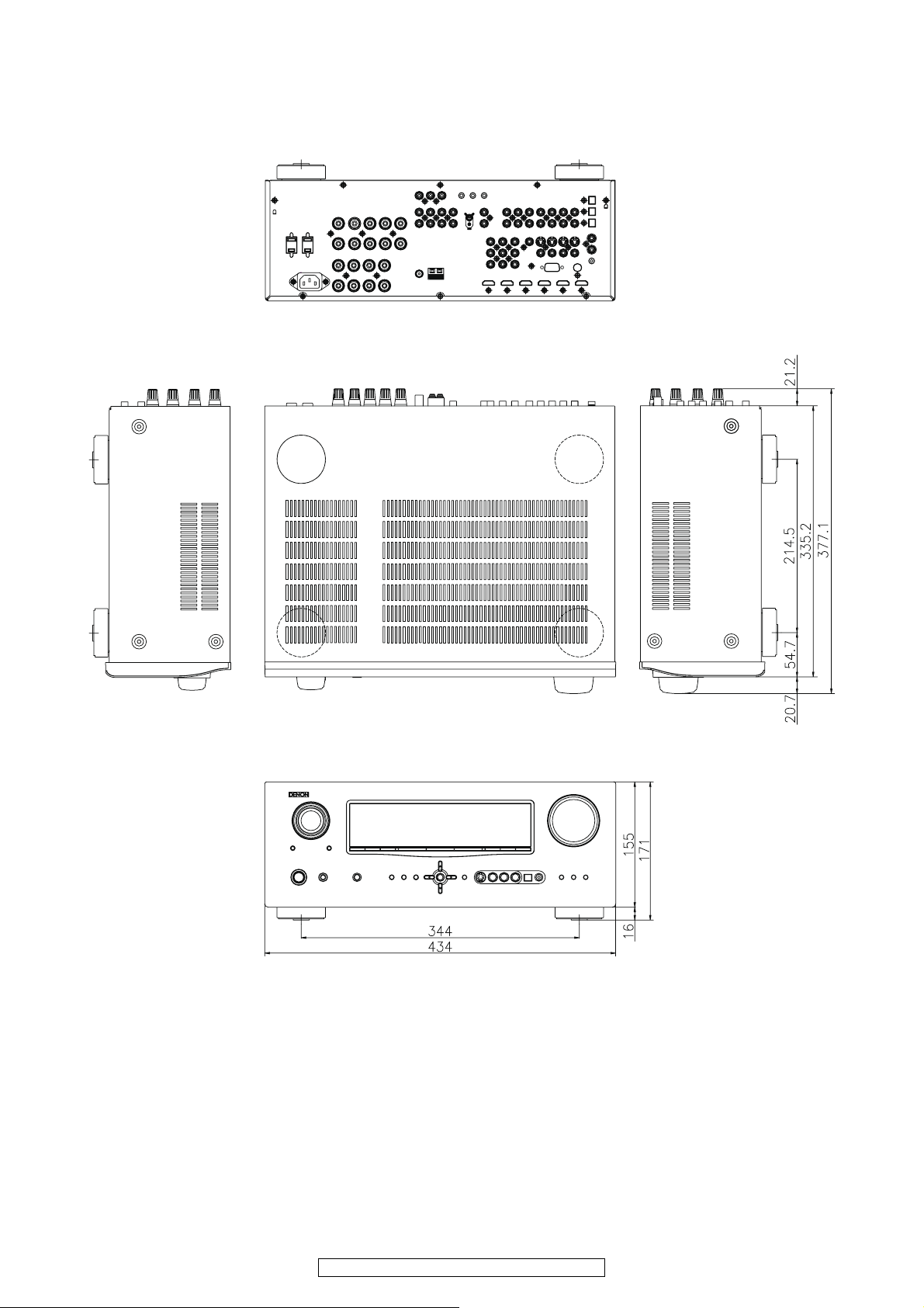
DIMENSION
AVR-2310CI/2310, AVC-2310 model
3
AVR-2310CI/2310/890, AVC-2310
Page 4
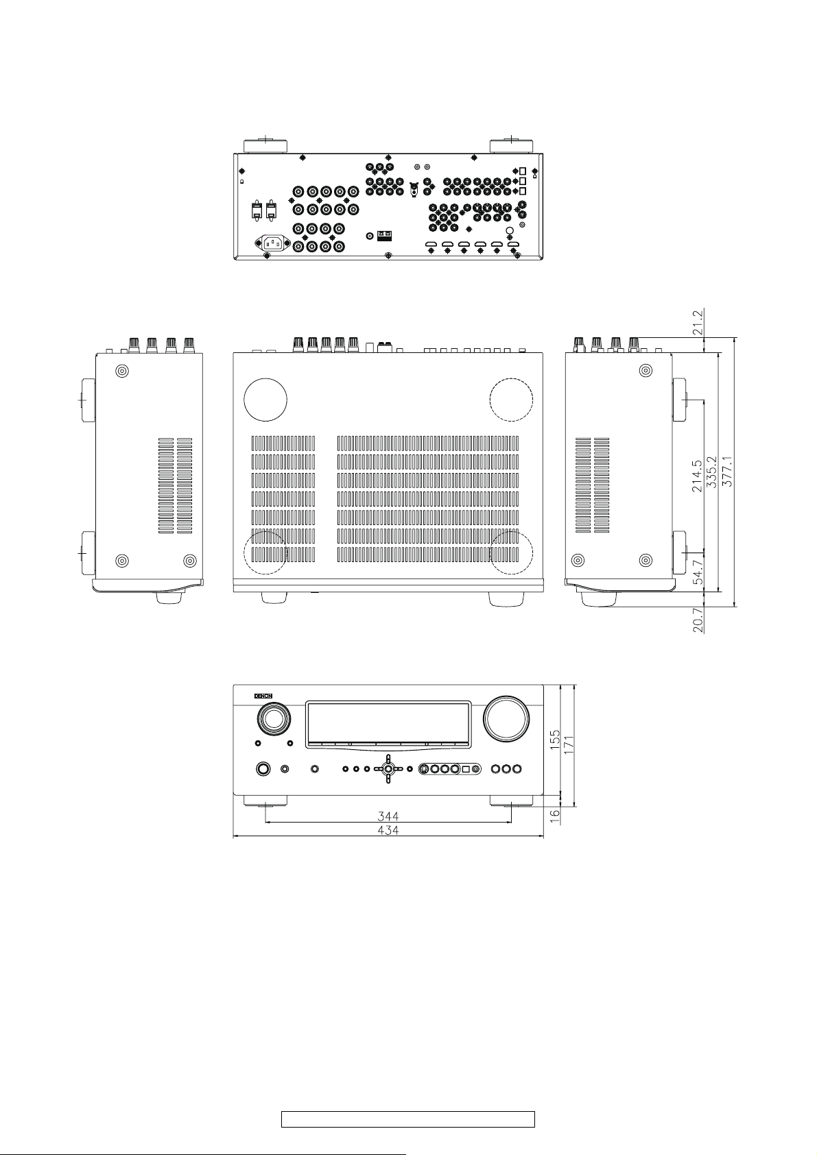
AVR-890 model
4
AVR-2310CI/2310/890, AVC-2310
Page 5
WIRE ARRANGEMENT
Back Panel side
Front Panel side
If wire bundles are untied or moved to perform adjustment or parts replacement etc., be sure to rearrange them neatly as
they were originally bundled or placed afterward.
Otherwise, incorrect arrangement can be a cause of noise
generation.
Wire arrangement viewed from the top
5
AVR-2310CI/2310/890, AVC-2310
Page 6
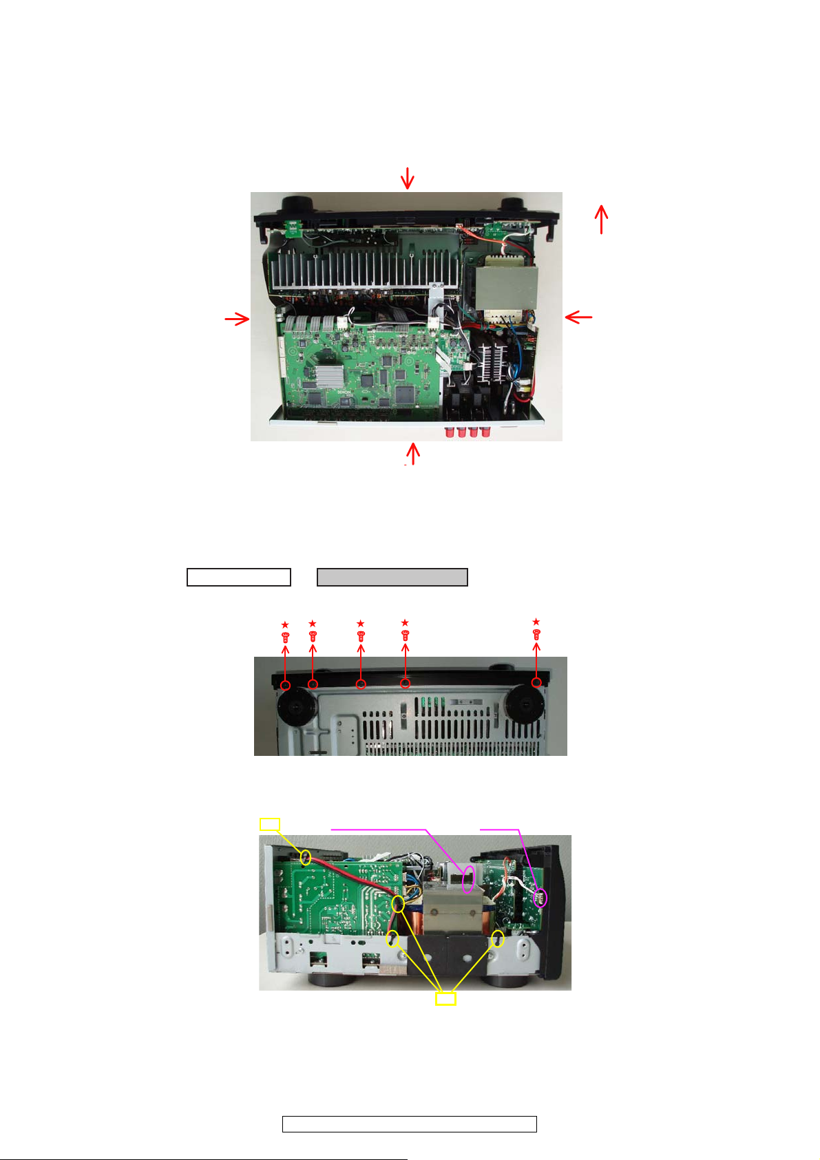
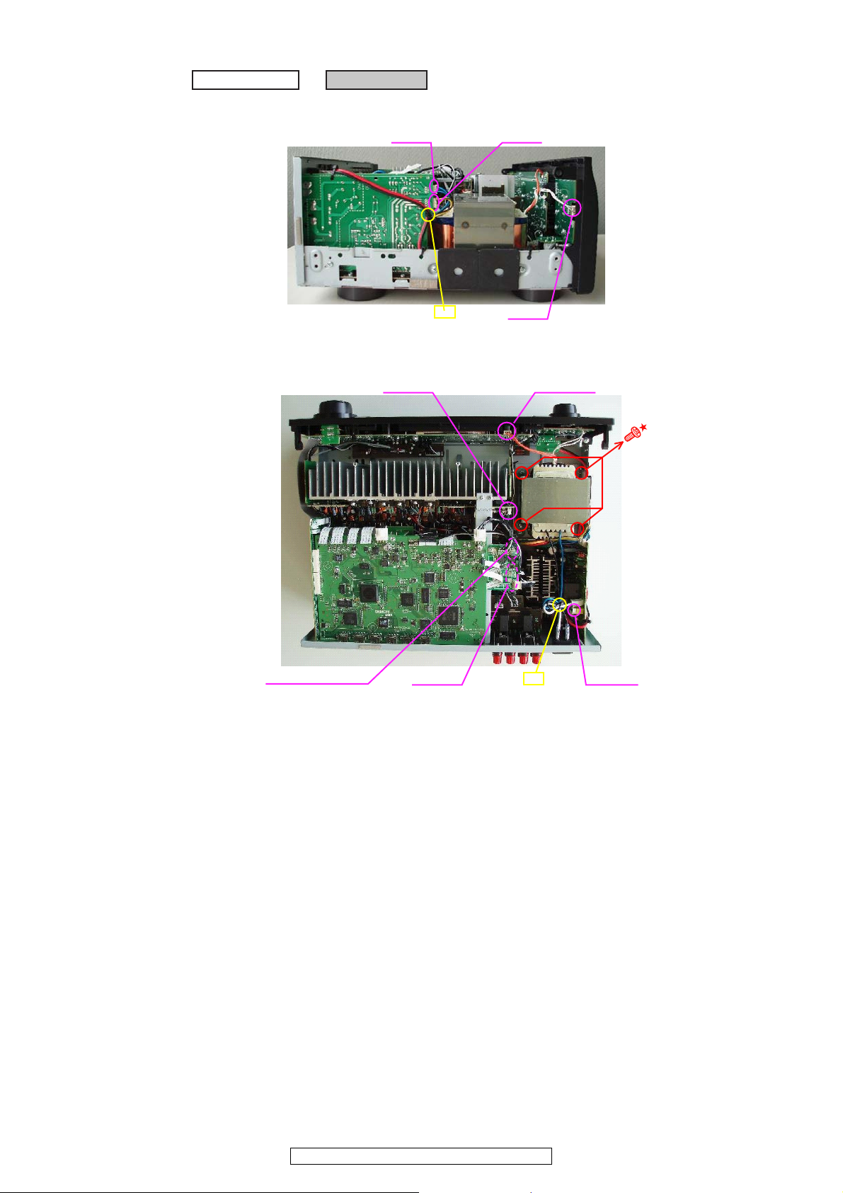
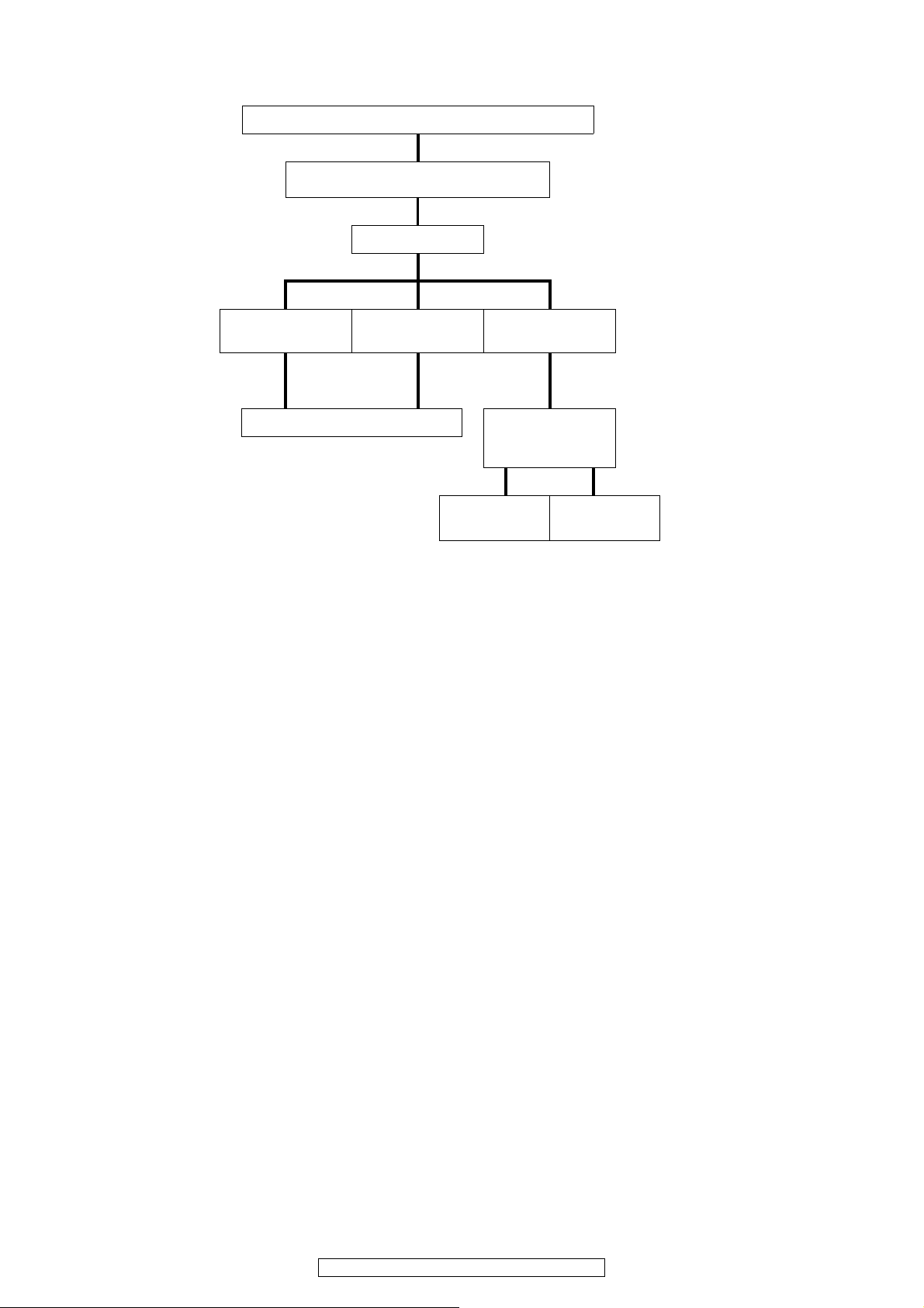
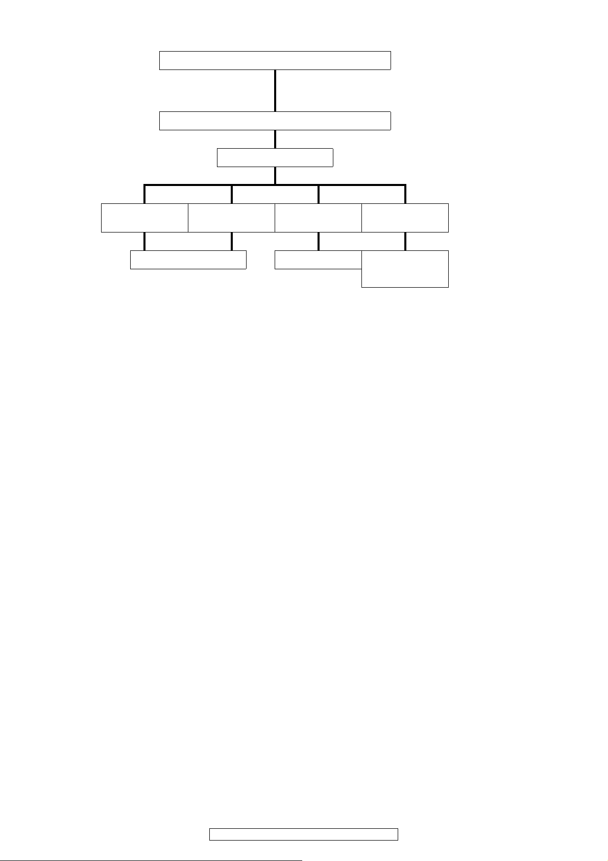
DISASSEMBLY
CABINET TOP
PANEL FRONT ASSY PCB HDMI ASSY
Refer to "DISASSEMBLY 1.PANEL FRONT ASSY" Refer to "DISASSEMBL 2.PCB HDMI ASSY"
and "EXPLODED VIEW" and "EXPLODED VIEW"
PCB S/W PCB HDMI ASSY
(Ref. No. of EXPLODED VIEW : B1) (Ref. No. of EXPLODED VIEW : B23)
PCB FUNCTION ENCORDER
(Ref. No. of EXPLODED VIEW : B2)
PCB FRONT
PCB DIGI-CNT ASSY BRACKET HDMI
(Ref. No. of EXPLODED VIEW : B3)
Refer to "DISASSEMBL 4.PCB DIGI-CNT ASSY" Refer to "DISASSEMBLY 3.BRACKET HDMI"
PCB H/P and "EXPLODED VIEW" and "EXPLODED VIEW"
䇭 (Ref. No. of EXPLODED VIEW : B4) PCB DIGI-CNT ASSY BRACKET HDMI
PCB V.AUX (Ref. No. of EXPLODED VIEW : B24) (Ref. No. of EXPLODED VIEW : 42)
(Ref. No. of EXPLODED VIEW : B5) PCB DIGI_POWER ASSY
PCB FUNCTION
TUNER PAC
K
(Ref. No. of EXPLODED VIEW : B32)
(Ref. No. of EXPLODED VIEW : B6)
Refer to "DISASSEMBL 5.TUNER PACK"
PCB CNT FUNCTION and "EXPLODED VIEW"
(Ref. No. of EXPLODED VIEW : B7) TUNER PACK
PCB ENCORDER (Ref. No. of EXPLODED VIEW : 36)
(Ref. No. of EXPLODED VIEW : B8)
PCB CNT ENCORDER E2/E2A/E1C model
(Ref. No. of EXPLODED VIEW : B9)
CHASSIS BAC
K
PCB PRE OUT ASS
Y
Refer to "DISASSEMBLY 6.CHASSIS BACK" Refer to "DISASSEMBL 14.PCB PRE OUT ASSY"
and "EXPLODED VIEW" and "EXPLODED VIEW"
TRANS MAIN
CHASSIS BACK PCB PRE OUT ASSY
Refer to "DISASSEMBLY 13.TRANS MAIN" (Ref. No. of EXPLODED VIEW : 34) (Ref. No. of EXPLODED VIEW : B25)
and "EXPLODED VIEW" PCB SPK
TRANS MAIN 䇭 (Ref. No. of EXPLODED VIEW : B17)
(Ref. No. of EXPLODED VIEW : 30) PCB SPK2
(Ref. No. of EXPLODED VIEW : B18)
PCB SPK_CNT
(Ref. No. of EXPLODED VIEW : B19)
PCB SIRIUS ASSY PCB SUPPLY and PCB POWER
Refer to "DISASSEMBL 7.PCB SIRIUS ASSY" Refer to "DISASSEMBLY 12.PCB SUPPLY
and "EXPLODED VIEW" and PCB POWER" and "EXPLODED VIEW"
PCB SIRIUS ASSY PCB SUPPLY (Ref. No. of EXPLODED VIEW : B13)
(Ref. No. of EXPLODED VIEW : B26) PCB POWER (Ref. No. of EXPLODED VIEW : B14)
PCB VIDEO ASSY
Refer to "DISASSEMBL 8.PCB VIDEO ASSY"
and "EXPLODED VIEW"
PCB VIDEO ASSY
(Ref. No. of EXPLODED VIEW : B23)
PCB INPUT ASSY
Refer to "DISASSEMBL 9.PCB INPUT ASSY"
and "EXPLODED VIEW"
PCB INPUT ASSY
( Ref. No. of EXPLODED VIEW : B21)
PCB CNT1 (Ref. No. of EXPLODED VIEW : B30)
PCB CPU ASSY
Refer to "DISASSEMBL 10.PCB CPU ASSY"
and "EXPLODED VIEW"
PCB CPU ASSY
( Ref. No. of EXPLODED VIEW : B27)
PCB MAIN ASSY
Refer to "DISASSEMBL 11.PCB MAIN ASSY"
and "EXPLODED VIEW"
PCB MAIN ASSY
( Ref. No. of EXPLODED VIEW : B20)
PCB 2CH ASSY
( Ref. No. of EXPLODED VIEW : B11)
PCB CNT3
( Ref. No. of EXPLODED VIEW : B28)
PCB CNT2
( Ref. No. of EXPLODED VIEW : B29)
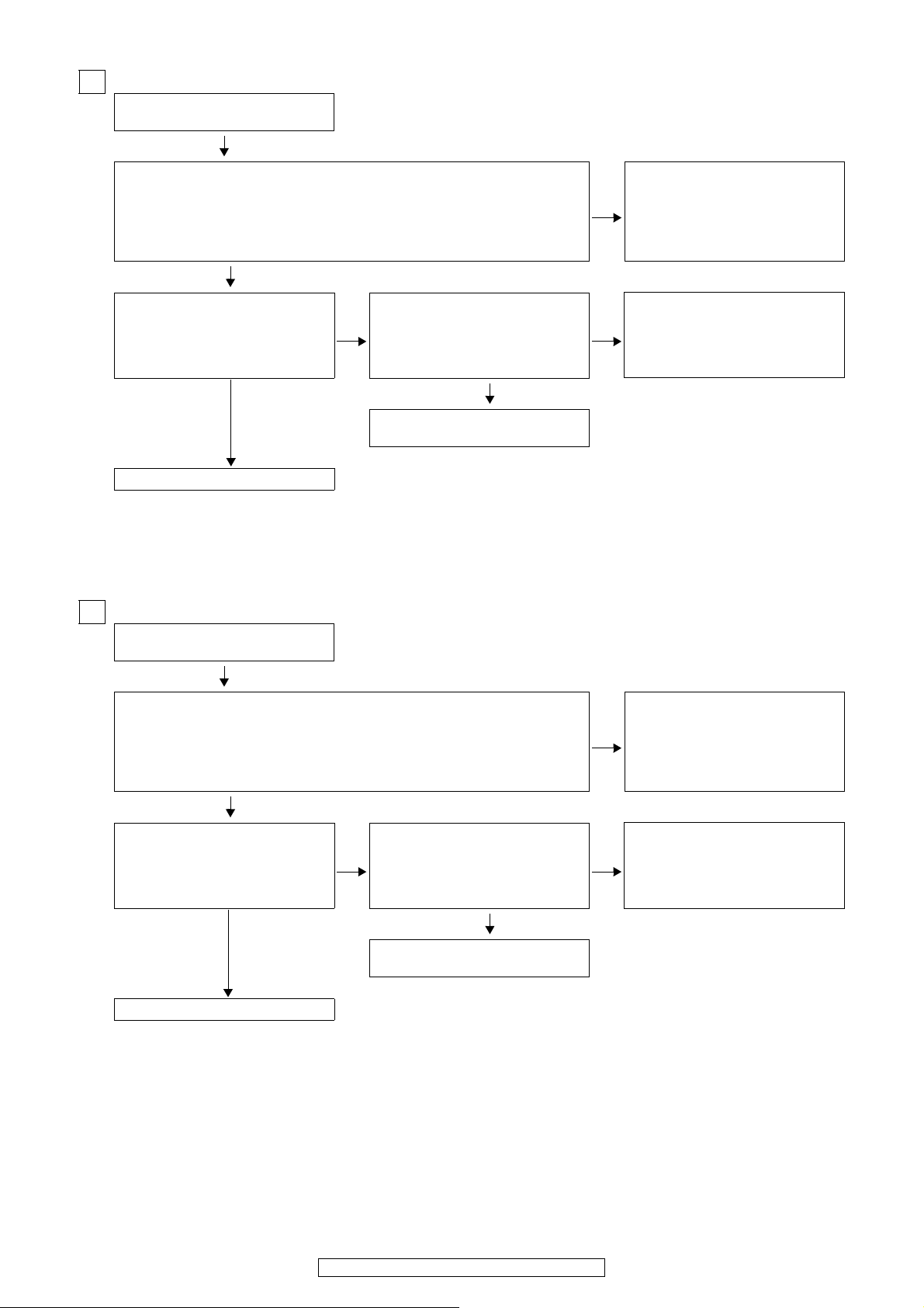
• Disassemble in order of the arrow of the figure of following flow.
• In the case of the re-assembling, assemble it in order of the reverse of the following flow.
• In the case of the re-assembling, observe "attention of assembling" it.
6
AVR-2310CI/2310/890, AVC-2310
Page 7
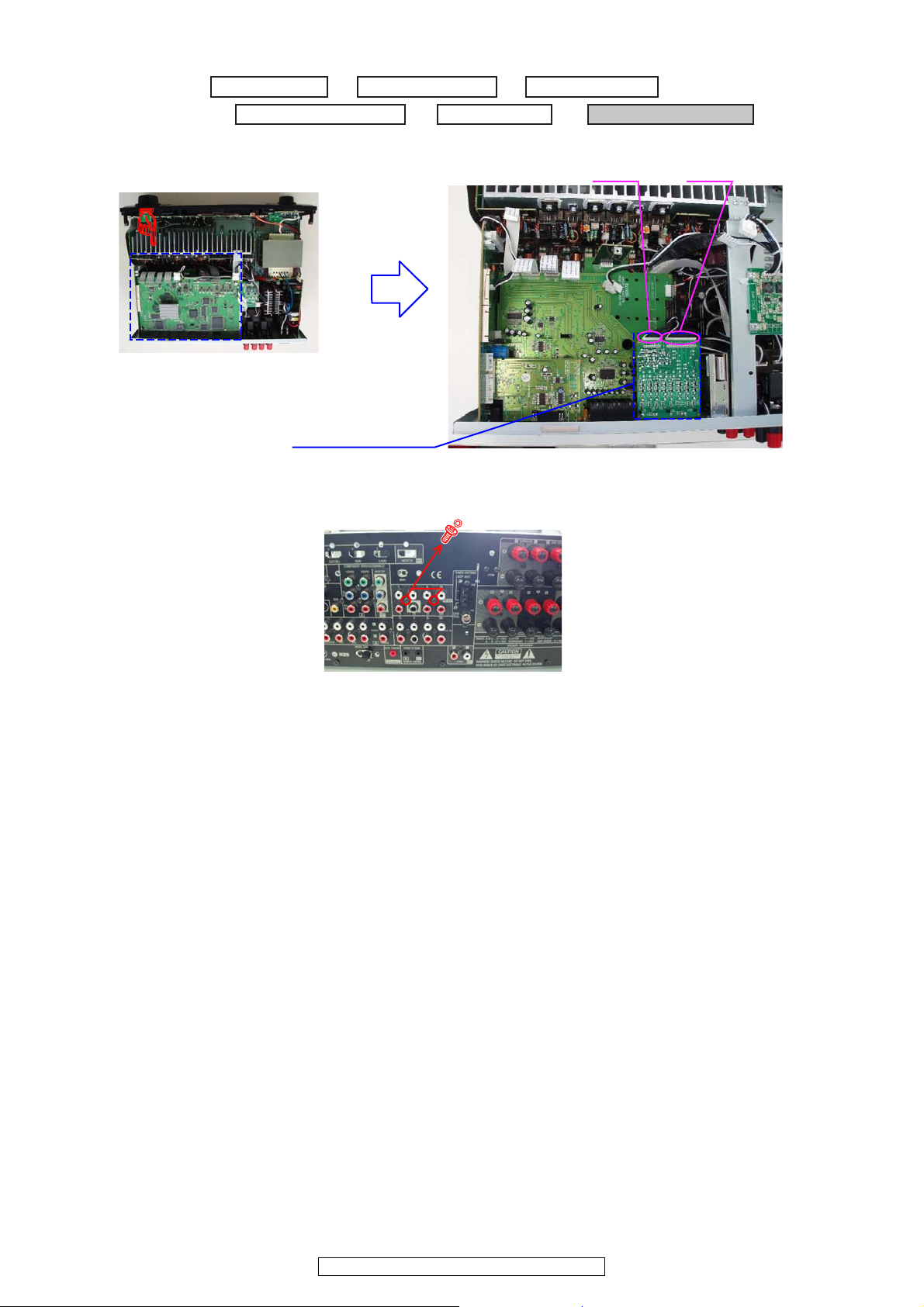
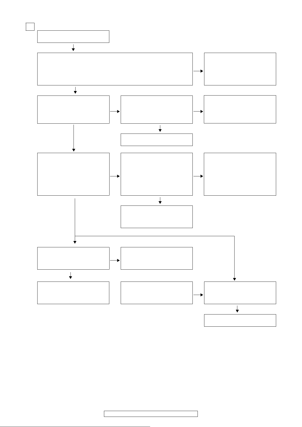
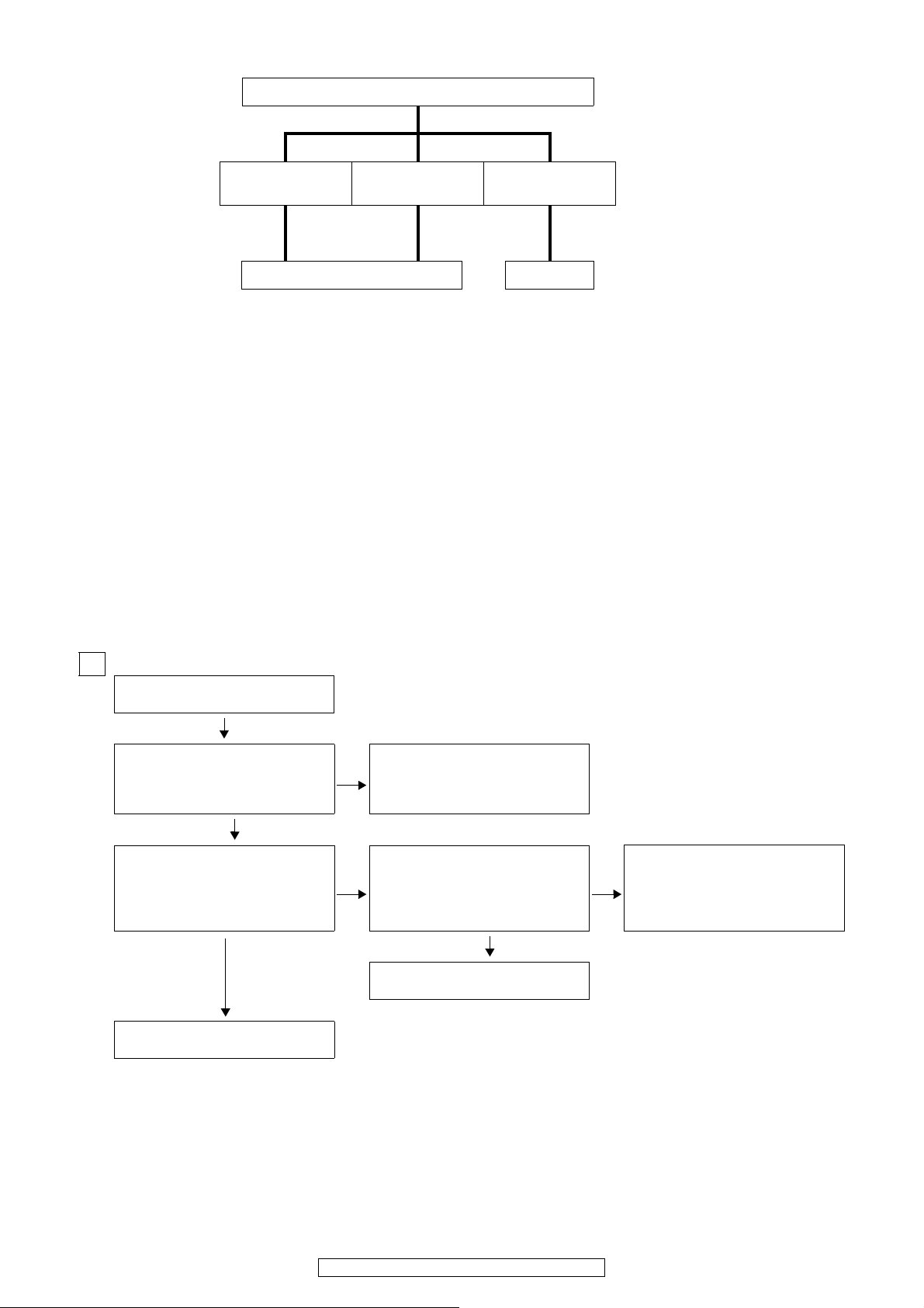
About the photos used for descriptions in the “DISASSEMBLY” section.
The viewpoint of each photograph
(Photografy direction)
[View from above]
Front side
Direction of photograph: B
Direction of photograph: D
Direction of photograph: C
Proceeding : CABINET TOP PANEL FRONT ASSY
→
Proceeding : CABINET TOP PANEL FRONT ASSY
→
View from bottom
Direction of photograph: D
Style pin : Loose CP301
cut
cut
• The direction from which the photographs used herein were photograph ed is indicated at "Direction of photograph: ***" at
the left of the respective photographs.
• Refer to the table below for a description of the direction in which the photos were taken.
• Photographs for which no direction is indicated were taken from above the product.
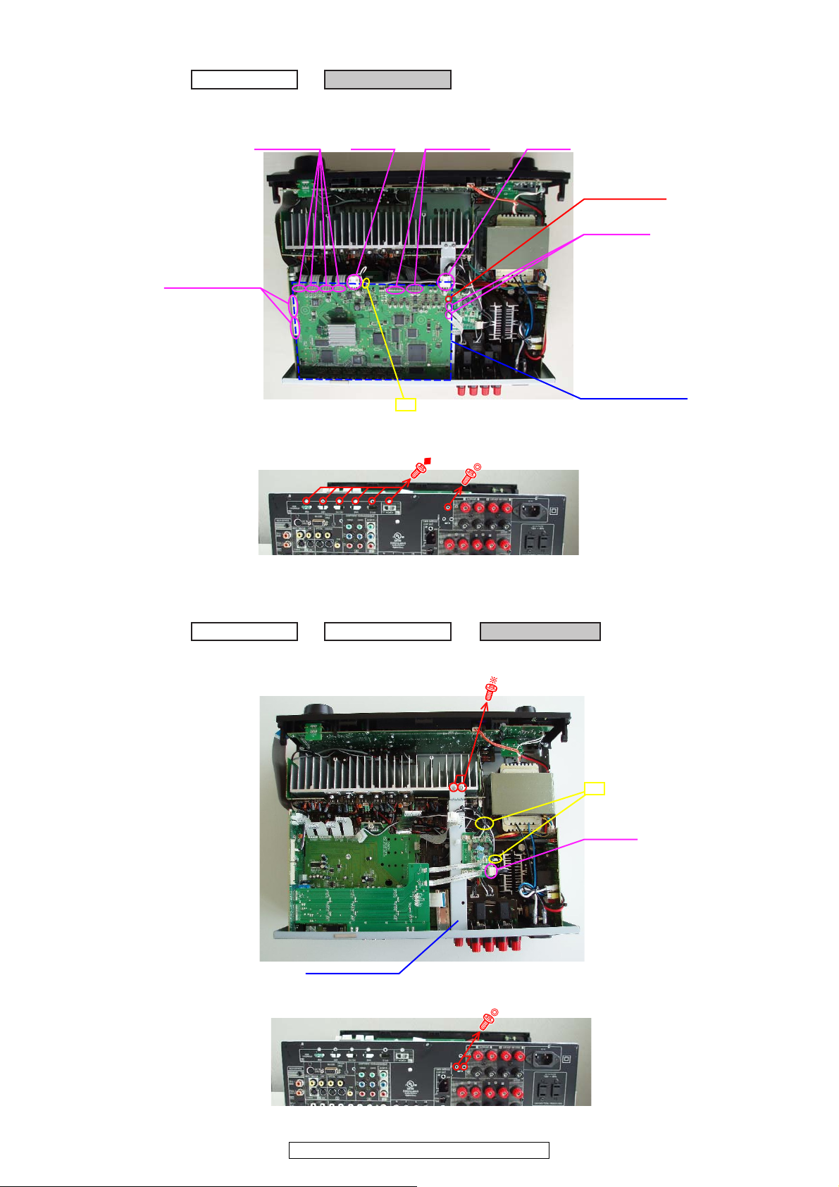
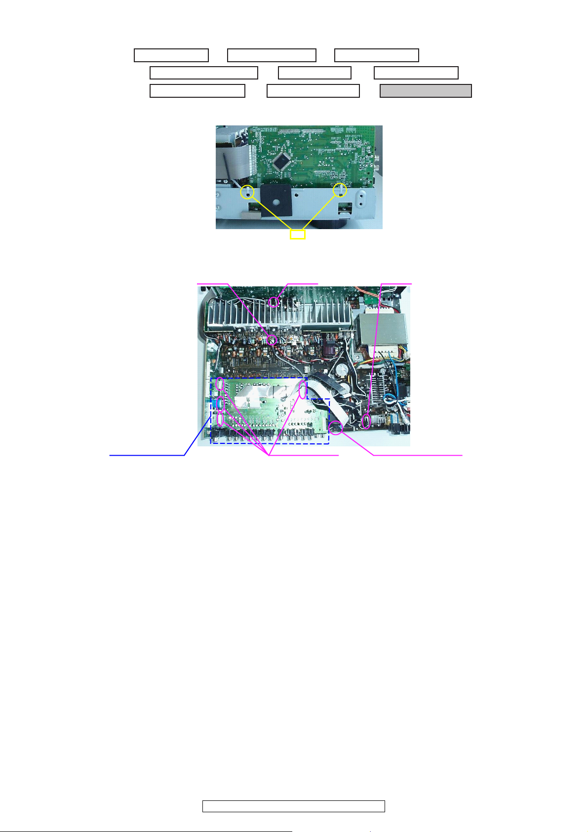
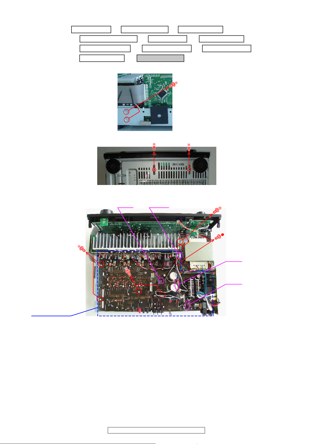
1. PANEL FRONT ASSY
(1) Remove the screws.
(2) Cut the wire clamp bands, then loose the style pin. Disconnect the connector wire.
AVR-2310CI/2310/890, AVC-2310
7
Page 8
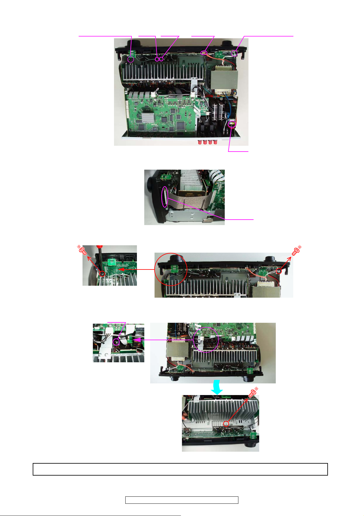
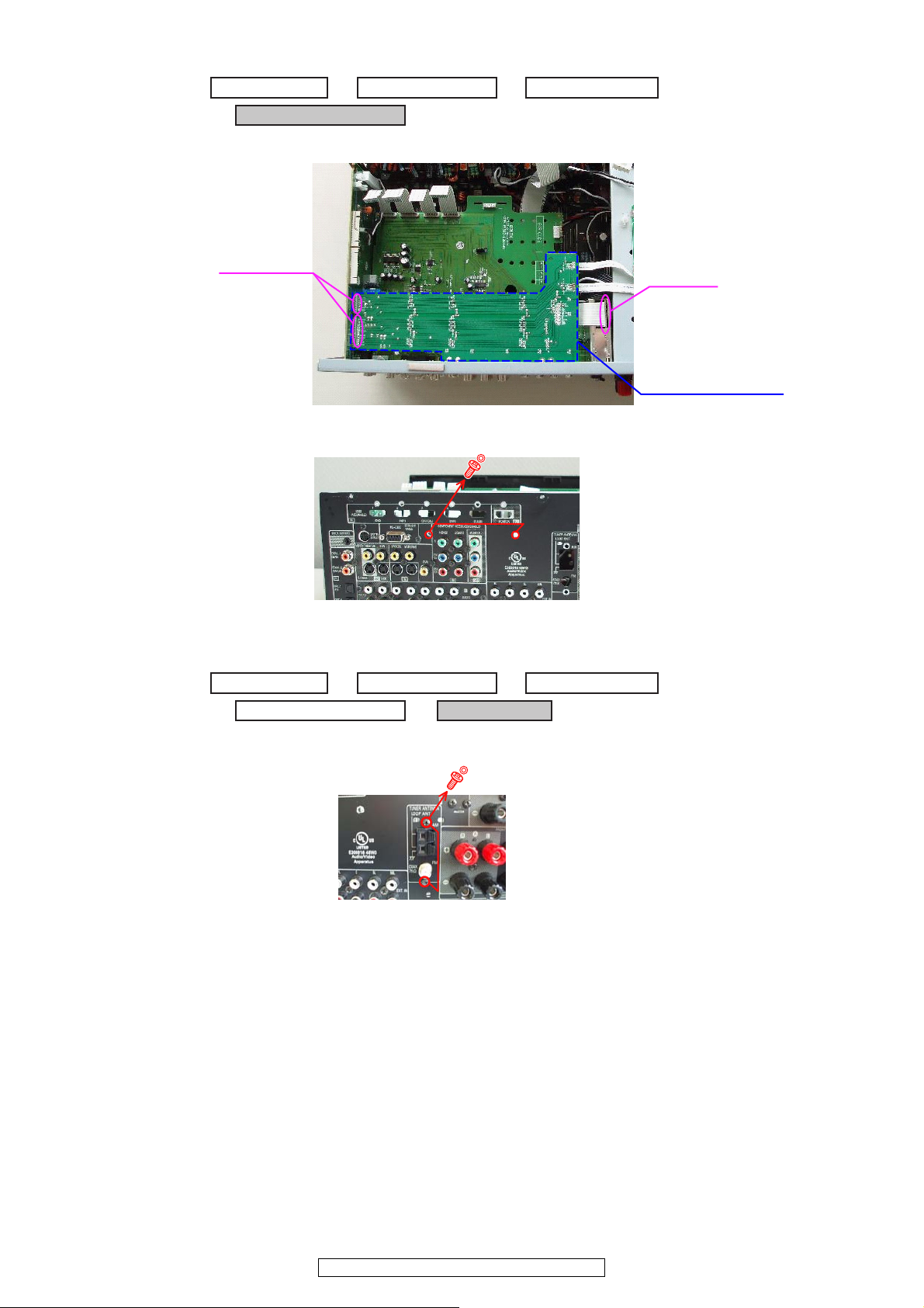
(3) Loose the Cord holders, then disconnect the connector wires.
Cord holder : Loose CN306A
CN305 CN303
CP503
Cord holder : Loose
Direction of photograph: C
FFC Cable
CP541
Direction of photograph: D
Please refer to "EXPLODED VIEW" for the disassembly method of each P.W.B included in PANEL FRONT ASSY.
(4) Disconnect the FFC Cable.
(5) Remove the screws.
(6) Disconnect the connector wire, then remove the screw.
8
AVR-2310CI/2310/890, AVC-2310
Page 9
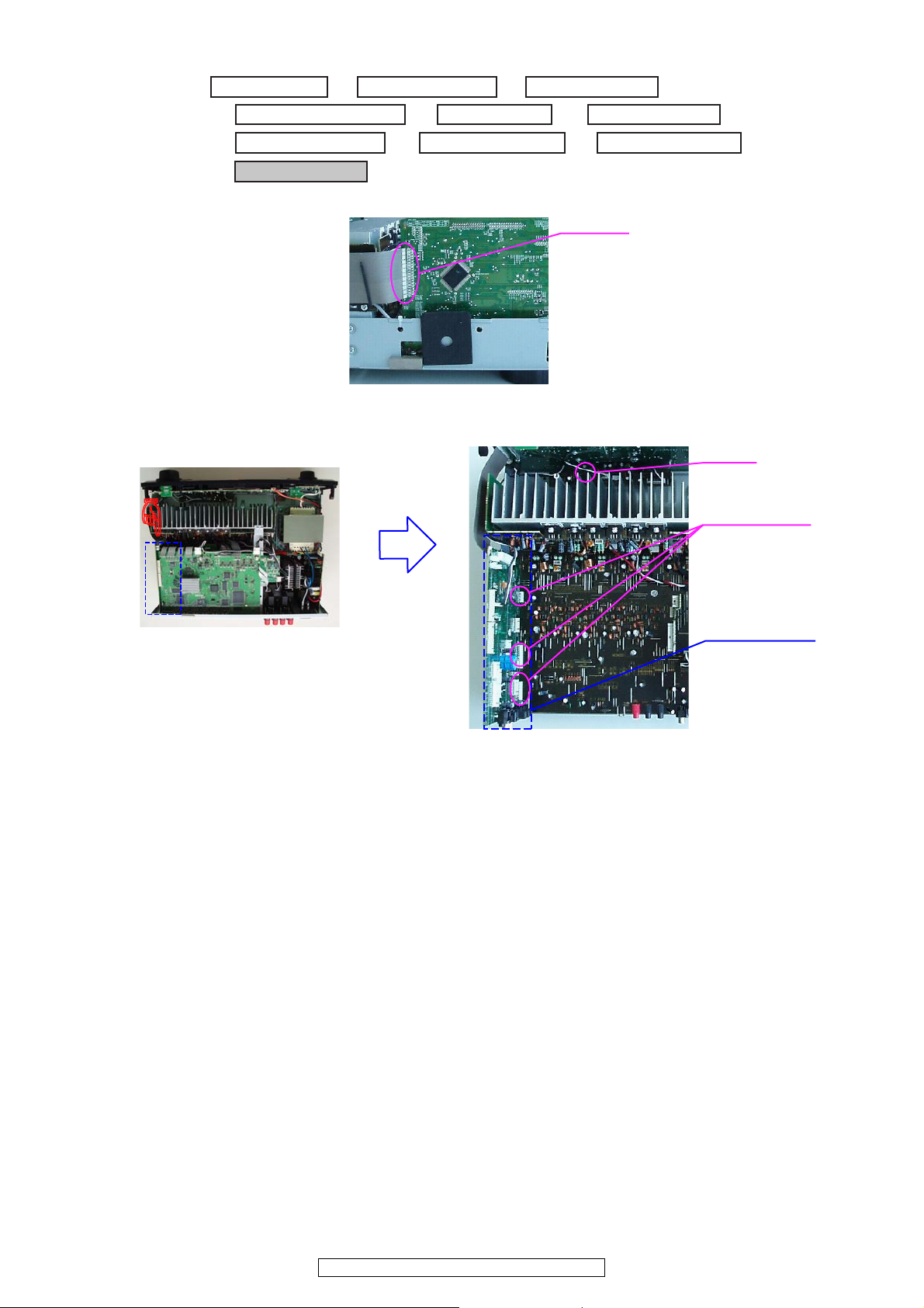
2. PCB HDMI ASSY
Proceeding : CABINET TOP HDMI PWB ASSY
→
PCB HDMI ASSY
Board to board
FFC Cable FFC Cable CX047
FFC Cable
SUPPORTER
CX046
cut
Direction of photograph: A
Proceeding : CABINET TOP HDMI PWB ASSY
→
BRACKET HDMI
→
CP2270
BRACKT HDMI
cut
Direction of photograph: A
(1) Cut the wire clamp band, then disconnect the connector wires and FFC Cables.
Remove the SUPPORTER, then disconnect the board to board.
(2) Remove the screws.
3. BRACKET HDMI
(1) Cut the wire clamper, then disconnect the connector wire. Remove the screws.
(2) Remove the screws.
AVR-2310CI/2310/890, AVC-2310
9
Page 10
4. PCB DIGI-CNT ASSY
Proceeding : CABINET TOP HDMI PWB ASSY
→
→
DIGI-CNT PWB ASSY
BRACKET HDMI
→
FFC Cable
Board to board
PCB DIGI-CNT ASSY
Direction of photograph: A
→
TUNER PACK
Proceeding : CABINET TOP HDMI PWB ASSY
→
→
DIGI-CNT PWB ASSY
BRACKET HDMI
→
Direction of photograph: A
(1) Disconnect the FFC cable and board to board.
(2) Remove the screws.
5. TUNER PACK
(1) Remove the screws.
AVR-2310CI/2310/890, AVC-2310
10
Page 11
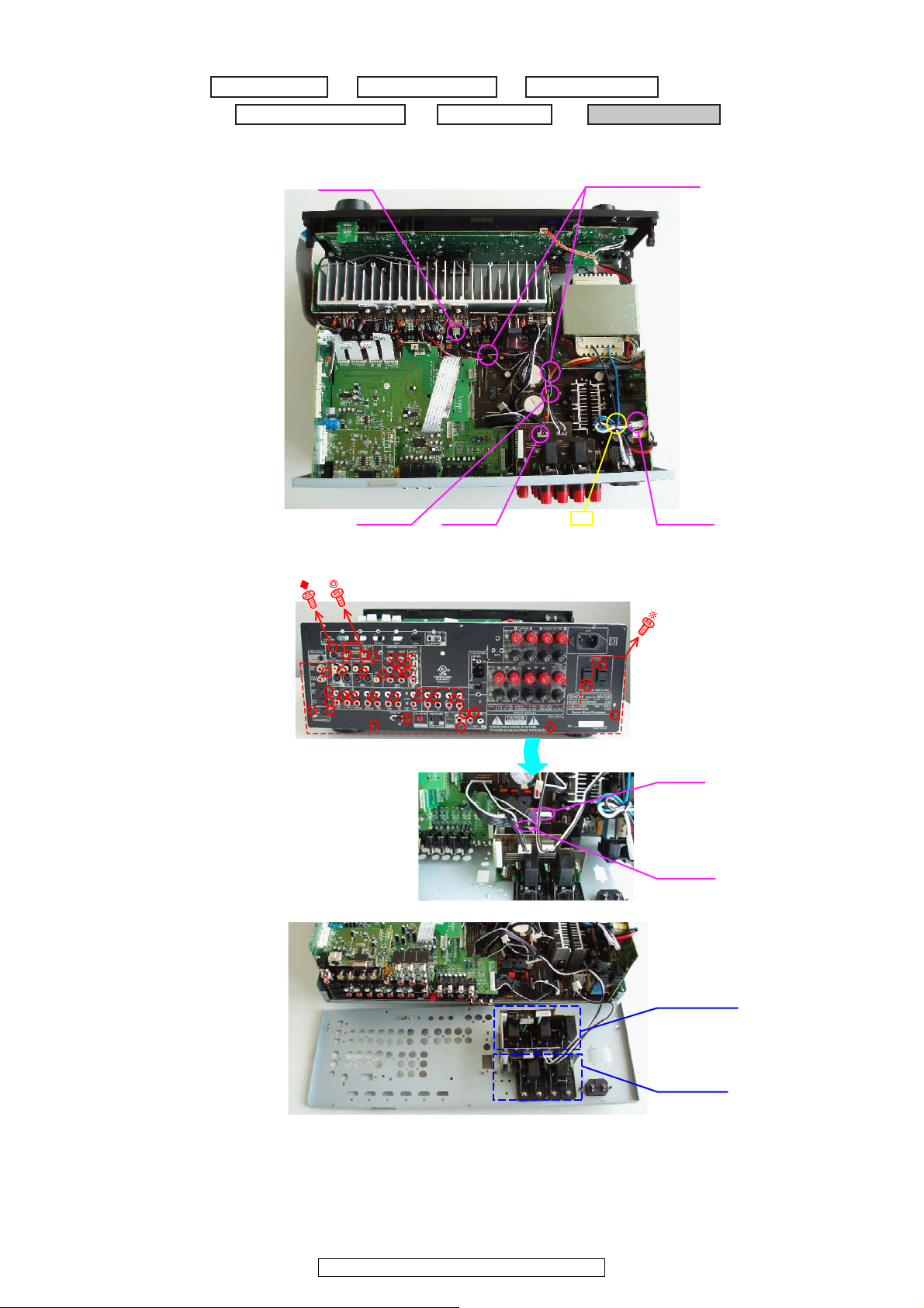
6. CHASSIS BACK
→
TUNER PACK
→
CHASSIS BACK
Proceeding : CABINET TOP HDMI PWB ASSY
→
→
DIGI-CNT PWB ASSY
BRACKET HDMI
→
Style pin : Loose
CP102B
CN101BCN102 CP501
cut
Direction of photograph: A
PCB SPK 2
PCB SPK
CP103
CP101A
(1) Cut the wire clamp band, then loose the style pins. Disconnect the connector wires.
(2) Remove the screws, then disconnect the connector wires.
AVR-2310CI/2310/890, AVC-2310
11
Page 12
7. PCB SIRIUS ASSY
→
TUNER PACK
→
CHASSIS BACK
Proceeding : CABINET TOP HDMI PWB ASSY
→
→
DIGI-CNT PWB ASSY
→
PCB SIRIUS ASSY
BRACKET HDMI
→
v
Board to board
PCB DSIRIUS ASSY
→
TUNER PACK
→
CHASSIS BACK
Proceeding : CABINET TOP HDMI PWB ASSY
→
→
DIGI-CNT PWB ASSY
→
PCB SIRIUS ASSY
→
PCB VIDEO ASSY
BRACKET HDMI
→
v
Board to board
PCB VIDEO ASSY
(1) Disconnect the board to board.
8. PCB VIDEO ASSY
(1) Disconnect the board to boards.
AVR-2310CI/2310/890, AVC-2310
12
Page 13
9. PCB INPUT ASSY
→
TUNER PACK
→
CHASSIS BACK
Proceeding : CABINET TOP HDMI PWB ASSY
→
→
DIGI-CNT PWB ASSY
→
PCB SIRIUS ASSY
→
PCB VIDEO ASSY
→
PCB INPUT ASSY
BRACKET HDMI
→
Direction of photograph: C
cut
PCB INPUT ASSY
Board to board Cord holder : LOOSE
CP515CN303CP708
(1) Cut the wire clamp bands.
(2) Loose the Cord holder, then disconnect the connector wires and board to board.
AVR-2310CI/2310/890, AVC-2310
13
Page 14
10. PCB CPU ASSY
→
TUNER PACK
→
CHASSIS BACK
Proceeding : CABINET TOP HDMI PWB ASSY
→
→
DIGI-CNT PWB ASSY
→
PCB SIRIUS ASSY
→
PCB VIDEO ASSY
→
PCB INPUT ASSY
→
PCB CPU ASSY
BRACKET HDMI
→
Direction of photograph: C
FFC Cable
v
Board to board
CN305
PCB CPU ASSY
(1) Disconnect the FFC cable.
(2) Disconnect the connector wires and board to board.
AVR-2310CI/2310/890, AVC-2310
14
Page 15
11. PCB MAIN ASSY
→
TUNER PACK
→
CHASSIS BACK
Proceeding : CABINET TOP HDMI PWB ASSY
→
→
DIGI-CNT PWB ASSY
→
PCB SIRIUS ASSY
→
PCB VIDEO ASSY
→
PCB INPUT ASSY
→
PCB CPU ASSY
→
PCB MAIN ASSY
BRACKET HDMI
→
Direction of photograph: C
View from bottom
CP2270CP541
CP104
CP511
PCB MAIN ASSY
(1) Remove the screws.
(2) Disconnect the connector wires, then remove the screws.
AVR-2310CI/2310/890, AVC-2310
15
Page 16
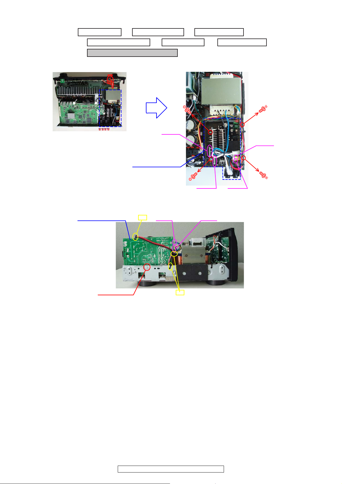
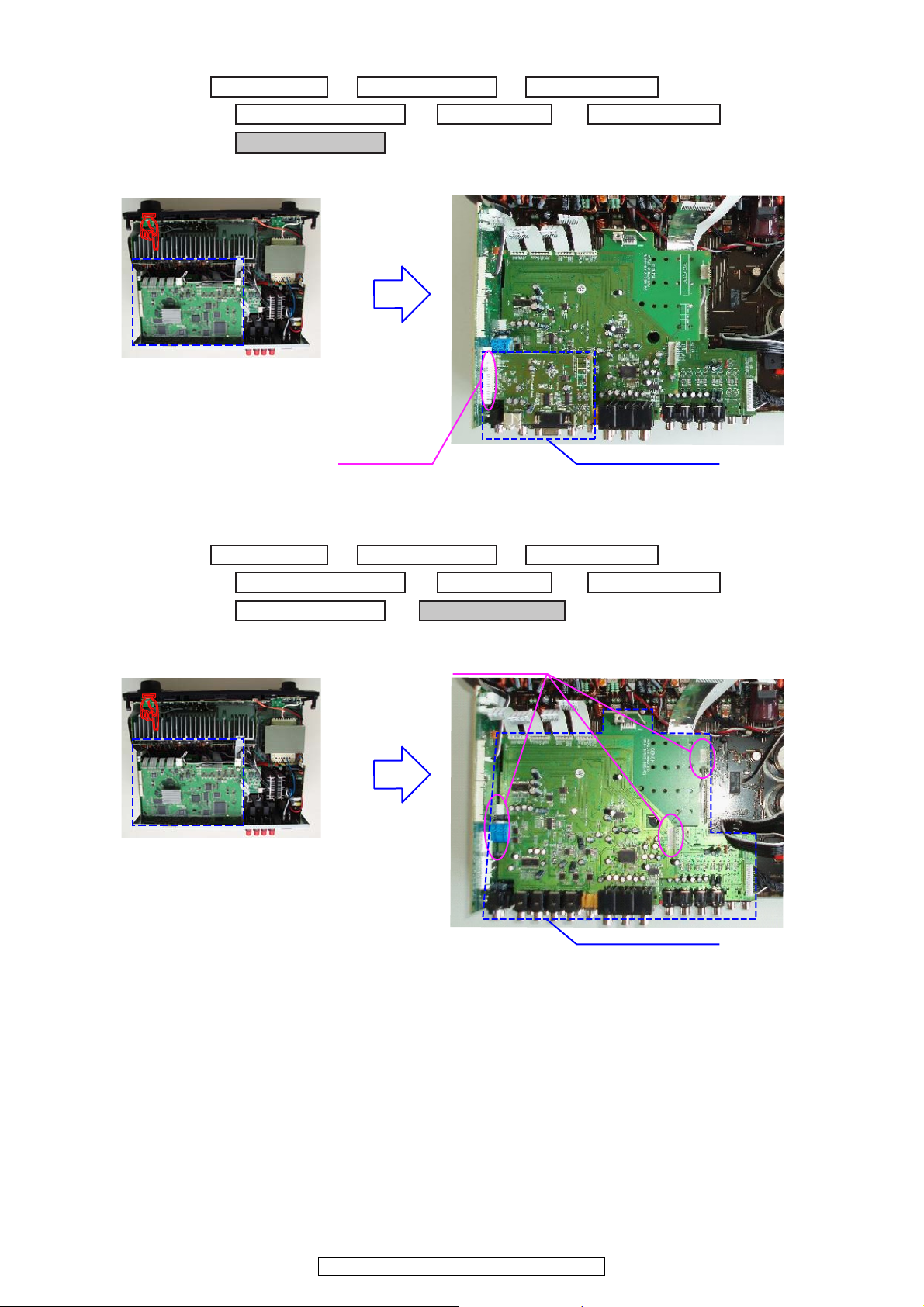
12. PCB SUPPLY and PCB POWER
→
TUNER PACK
→
CHASSIS BACK
Proceeding : CABINET TOP HDMI PWB ASSY
→
→
DIGI-CNT PWB ASSY
→
PCB SUPPLY and PCB POWER
BRACKET HDMI
→
v
PCB SUPPLY ASSY
CP501
CP503CP511
CP515
Direction of photograph: D
SUPPORTER
CP513 CP512
cut
cut
PCB POWER ASSY
(1) Disconnect the connector wires, then remove the screws.
(2) Cut the wire clamp bands, then disconnect the connector wires and SUPPORTER.
AVR-2310CI/2310/890, AVC-2310
16
Page 17
13. TRANS MAIN
Proceeding : CABINET TOP TRANS MAIN
→
Direction of photograph: D
CP513
CP301
CP512
cut
Style pin : Loose
CP2270 CN306A
CP104 CP501
cut
(1) Cut the wire clamp bands, then disconnect the connector wires and SUPPORTER.
(2) Cut the wire clamp band, then loose the style pin. Disconnect the connector wires, then remove the screws.
AVR-2310CI/2310/890, AVC-2310
17
Page 18
14. PCB PRE OUT ASSY (E2/EA/E1C model)
→
TUNER PACK
→
PCB PRE OUT ASSY
Proceeding : CABINET TOP HDMI PWB ASSY
→
→
DIGI-CNT PWB ASSY
BRACKET HDMI
→
v
CN702CN701
PCB PRE-OUT ASSY
Direction of photograph: A
(1) Disconnect the connector wires.
(2) Remove the screws.
AVR-2310CI/2310/890, AVC-2310
18
Page 19
CAUTION IN SERVICING
Note:・If step 3 does not work, start over from step 1.
・ All user settings will be lost and this factory setting will be recovered when this initialization mode.
So make sure to m+emorize your setting for restoring after the initialization.
SURROUND
MODE 0
SURROUND
MODE 1
ON/OFF
Initializing AV SURROUND RECEIVER
AV SURROUND RECEIVER initialization should be performed when the µcom, peripheral parts of µcom, and Digital P.W.B.
are replaced.
1. Switch off the unit.
2. With the "SURROUND MODE 0" and "SURROUND MODE 1" buttons pressed, press the "ON/OFF" button to turn the
power on.
3. Check that the entire display is flashing with an interval of about 1 second, and release your fingers from the 2 buttons and
the microprocessor will be initialized.
JIG to use for servicing
When you repair the printing board, you can use the following JIG (Extension cable kit). Please order to Denon Official Service
Distributor in your region if necessary.
00D SPK- 561 EXTENSION UNIT KIT : 1 Set
00D SPK- 562 9120 CONN. JOINT KIT : 1 Set
When you update the firmware, you can use the following
JIG (RS232C to internal connector conversion adapter with 8P cable kit ). Please order to Denon Official Service Distributor
in your region if necessary.
00DSPK-581 WRITING UNIT : 1 Set
AVR-2310CI/2310/890, AVC-2310
19
Page 20
SPECIAL MODE d
DYNAMIC
VOLUME
DYNAMIC
EQ
ENTER
MENU
SURROUND
0 MODE 1
ON/OFF
CURSOR
SOURCE
DIMMER
RESTORER
STATUS
MULTEQ
Special mode setting button
※ Press the ON/OFF button to turn on while pressing both buttons A and B at the same time.
Mode Button A Button B Contents
µcom/DSP Version display mode
Errors checking mode
(Displaying the protection history mode)
Initialization mode
Mode for switching tuner frequency step
Mode for preventing remote control
acceptance
Panel lock mode
Panel lock mode
(Remove Master volume)
Cancellation of panel lock mode MENU RESTORER Panel lock mode is cancelled.
STATUS DIMMER
STATUS MUL TEQ
SURROUND
MODE0
DYNAMICEQDYNAMIC
CURSOR 0 RESTORER
SURROUND
MODE0
SURROUND
MODE1
SURROUND
MODE1
VOL
RESTORER
RESTORER Operations using main unit panel buttons are rejected.
Serial No. and firmware versions such as Main, Sub, DSP are
displayed in the FL manager. Errors are displayed when they
occur. (Refer to 21 page.)
Displaying the protection history
(Refer to 22 page.)
Backup data initialization is carried out.
(Refer to 19 page.)
---E2 model only--Select with the SOURCE 0 1 button.
Change tuner frequency step to AM9k/FM50kHz STEP or AM:10k/
FM:200kHz.
Operations using remote control are rejected.
(Mode cancellation: Turn off power and execute the same button
operations as when performing setup.)
Operations using main unit panel buttons or master volume are
rejected.
20
AVR-2310CI/2310/890, AVC-2310
Page 21
1. µcom/DSP Version display mode
1.1. Operation specifications
µcom/DSP version display mode:
When started up, the version information is displayed.
Starting up:
With the "DIMMER" and "STATUS" buttons pressed, press the "ON/OFF" button to turn the power on.
Now, press the "STATUS" button to the display the 2nd item information on the FL Display.
1.2. Display Order
Destination information→Main-µcom version information →Sub-µcom version information → DSP version information
→ APLD version information → OSD config information → OSD PRG information→ OSD DAT information
1.3. Display
Any one of the following list is displayed, in the priority of ①②③④ .
Condition State Display
①
Sub-µcom NG
② DIR NG
③ DSP NG
④
Both SUB/DSP OK
No response from Sub-µcom
No response from DIR
When DSP boot, executing DSP reset makes no change to DSP FLAG 0
port "H".
No change to DSP FLAG 0 port "H" before issuing DSP command.
When DSP data read, executing WRITE="L" makes no change to
ACK="H".
When DSP data read, executing REQ="L" makes no change to
ACK="L".
When DSP data write, executing WRITE="H" makes no change to ACK="H".
When DSP data write, executing REQ="L" makes no change to
ACK="L".
When DSP special code boot, executing DSP reset makes no change to
DSP FLAG 0 port "H".
No change to DSP FLAG 0 port "H" before issuing DSP special read
command.
No change to DSP FLAG 0 port "H" before DSP version read.
" □ SUB □□ ERROR □01□ "
" □ DIR □□ ERROR □01□ "
" □ DSP □□ ERROR □01□ "
" □ DSP □□ ERROR □02□ "
" □ DSP □□ ERROR □03□ "
" □ DSP □□ ERROR □04□ "
" □ DSP □□ ERROR □05□ "
" □ DSP □□ ERROR □06□ "
" □ DSP □□ ERROR □11□ "
" □ DSP □□ ERROR □12□ "
" □ DSP □□ ERROR □13□ "
(No error display, version display only)
21
AVR-2310CI/2310/890, AVC-2310
Page 22
2. Errors checking mode (Displaying the protection history)
2.1. Operation specifications
Error mode (Displaying the protection history):
When started up, the error information is displayed.
Starting up:
● All model commonness
With the "STATUS" and "MULTEQ" buttons pressed, press the "ON/OFF" button to turn the power on. The error (protection
history display) mode is set.
Now, press the "STATUS" button to turn on the FL display.
2.2. About the display on the FL display
When the "STATUS" button is pressed after setting the error (protection history display) mode, a history like the one shown
below is displayed, depending on the conditions.
(1) Normally (when there has been no protection incident)
Upper P R O T E C T
Lower N O P R O T E C T
(2) For ASO/DC (when the last protection incident was ASO or DC protection)
Upper P R O T E C T
Lower P R T : A S O / D C
ISTORY
H
ISTORY
H
(3) For THERMAL (when the last protection incident was THERMALprotection)
Upper P R O T E C T
Lower P R T : T H E R M A L
ISTORY
H
When the "STATUS" button is pressed again after the above protection history is displayed, the normal display reappears.
2.3. Clearing the protection history
There are two ways to clear the protection history, as described below.
(1) Start up the error (protection display) mode, display the error, then press and hold in the "ENTER" button for 3 seconds.
Upper P R O T E C T
Lower : T H E R M A L T H E
Press and hold in the "ENTER" button for 3 seconds
Upper P R O T E C T
Lower P R T : C L E A R
The above is displayed and the protection history is cleared.
ISTORY
H
ISTORY
H
Upper P R O T E C T
Lower N O P R O T E C T
ISTORY
H
(2) Initialize.
※ If you want to save a backup, use the method in 3.(1) above.
Warning indication by the POWER LED
If the power is turned off when a protection incident has been detected, the POWER LED (red) flashes as a warning according to the conditions in which the protection incident occurred.
(1) ASO/DC PROTECTION : Flashes in cycles of 0.5 seconds (0.25 seconds lit, 0.25 seconds off)
(2) THERMAL PROTECTION : Flashes in cycles of 2 seconds (1 second lit, 1 second off)
22
AVR-2310CI/2310/890, AVC-2310
Page 23
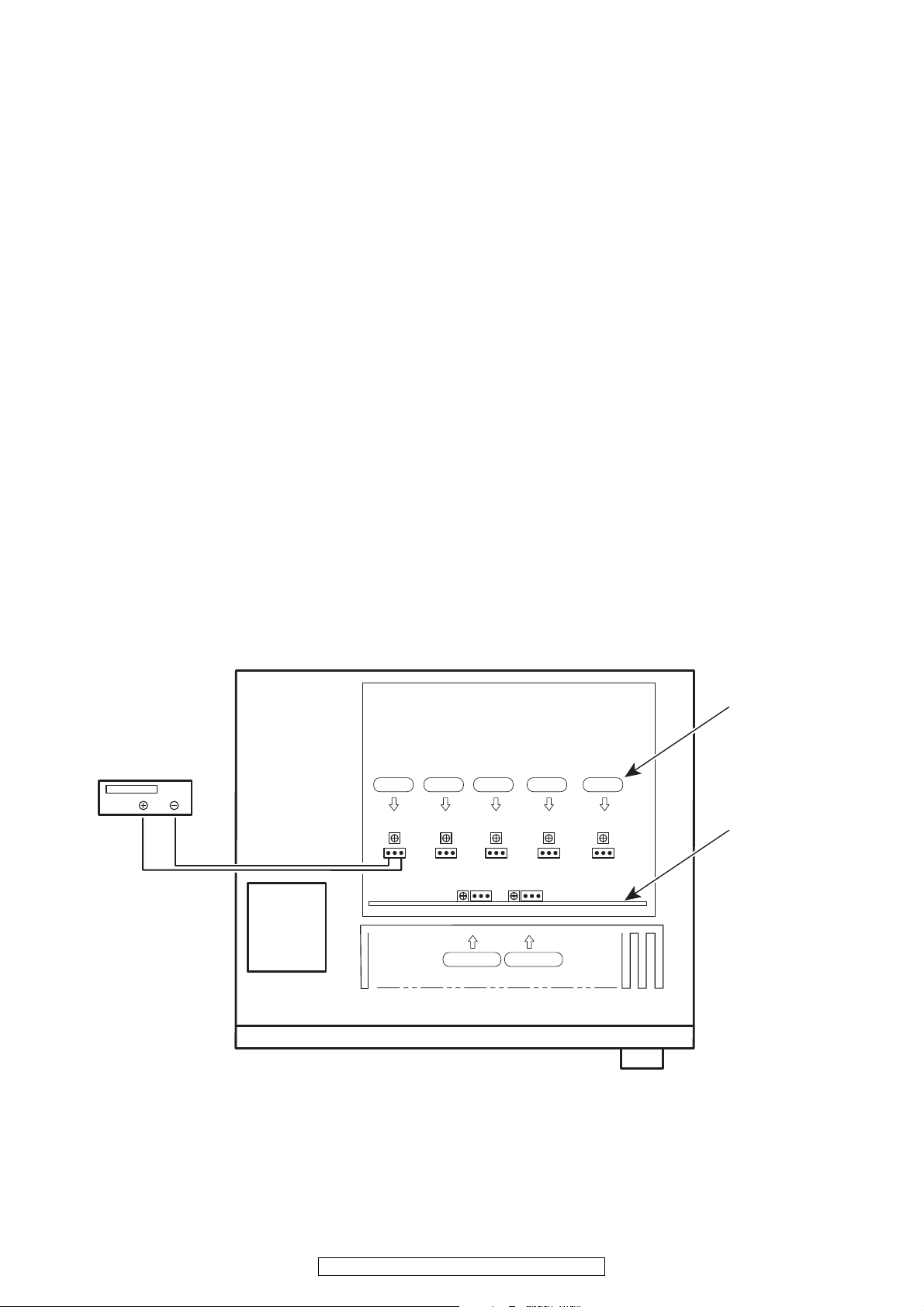
ADJUSTMENT
VR101SR
TP104
VR101FL
TP101
TP102
VR101SL
TP402
VR402
TP103
VR101C
VR101FR
TP105
F Lch
S Lch
S Back Rch
TP401
VR401
S Back Lch
C ch
S Rch
F Rch
DC Voltmeter
PCB MAIN ASSY
PCB 2CH ASSY
Audio Section
Idling Current
Required measurement equipment: DC Voltmeter
1. Preparation
(1) Avoid direct blow from an air conditioner or an electric fan, and adjust the unit at normal room temperature
15 °C ~ 30 °C (59 °F ~ 86 °F).
(2) Presetting
• POWER (Power source switch) OFF
• SPEAKER (Speaker terminal) No load
(Do not connect speaker, dummy resistor, etc.)
2. Adjustment
(1) Remove top cover and set VR101 FL, FR, C, SL, SR, on Main Amp. Unit, VR401, VR402 on 2ch- Amp.
Unit at fully counterclockwise (c) position.
(2) Connect DC Voltmeter to test points (FRONT-Lch: TP101, FRONT-Rch: TP105, CENTER ch: TP103, SURROUND-
Lch: TP102, SURROUND-Rch: TP104, SURROUND-BACK Lch: TP401, SURROUND-BACK Rch: TP402).
(3) Connect power cord to AC Line, and turn power switch "ON".
(4) Presetting.
MASTER VOLUME: "---" counterclockwise (c min.)
SPEAKER (Speaker terminal) : No load
(Do not connect speaker, dummy resistor, etc.)
MODE : 7CH STEREO (5CH STEREO)
FUNCTION : CD
(5) Within 2 minutes after the power on, turn VR101 clockwise (x) to adjust the TEST POINT voltage to 1.5 mV ± 0.5 mV
DC.
(6) After 10 minutes from the preset above, turn VR101 to set the voltage to 2.0 mV ± 0.5 mV DC.
(7) Adjust the Variable Resistors of other channels in the same way.
23
AVR-2310CI/2310/890, AVC-2310
Page 24
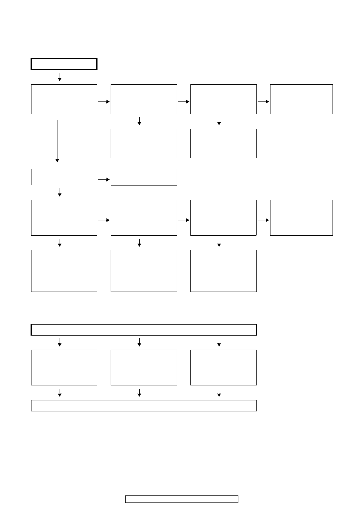
TROUBLE SHOOTING
1. POWER
1.1. Power not turn on
Power not turn on
YES
Is the ON/STANDBY indicator on the front panel flashing
red?
YES
Is the fuse blown?
YES
Does the power turn on when
the POWER switch is turned
off then back on?
YES YES YES
Check the primary circuitry
parts including the POWER
switch (for poor contacts,
etc.), and replace any defective parts.
Are there any incomplete
connections in the connec-
NO
tors connecting between the
various circuit boards?
YES YES
Connect the connectors
properly.
NO
NO
Refer to Fuse is blown
Is a DC 5V voltage being
supplied from the PCB
POWER (CN505 pin 4) to the
microprocessor?
Check the microprocessor
periphery circuitry and
replace any defective parts.
Is there a short circuit
NO
between the speaker terminals and the ground?
Check for damage in the
power amplifier circuitry parts
and replace any defective
parts.
Is a DC 5V voltage output
when the cord supplying the
NO
power from the PCB SUPPLY to the microprocessor
(CP511) is unplugged?
Check the circuitry and parts
from CP511 on the PCB
SUPPLY to the microprocessor for damage and short-circuits, and replace any
defective parts.
Correct the short circuit
NO
between the speaker and
the ground.
Check the parts from IC501
NO
to the primary circuitry and
replace any defective parts.
1.2. Fuse is blown
YES YES YES
Check for leaks or short circuits in the primary side
parts, and replace any defective parts.
YES YES YES
Fuse is blown
Check for short circuits in the
rectifier diodes and circuitry
of the secondary side rectifying circuits, and replace any
defective parts.
After repairing, also replace the fuse.
Check for short circuits in the
power stabilizer unit's regulator output terminal and the
ground, and replace any
defective parts.
24
AVR-2310CI/2310/890, AVC-2310
Page 25
2. Analog video
2.1. MONITOR OUT
MONITOR OUT (CVBS/S/COMPONENT) output NG
Check the Video convert ON/OFF settings
Video convert ON
Input
CVBS
A Interlace
Input
S
Inpu t
COMPONENT
Progressive
Interlace
B
※ When checking operation, select
SAT/CBL for the function of CVBS/
S, and select DVD for the function
of COMPONENT.
(COMPONENT1 input)
or
Progressive
no output
25
AVR-2310CI/2310/890, AVC-2310
Page 26
A
Check Power Supply Voltages.
Input
CVBS/S
V+5 : CN2005-8pin
V-5 : CN2005-7pin
SCPU+5V : CY141-1pin
CEC3.3V : C420 (IC402 side)
CEC1.8V : C428 (IC403 side)
OK
PCB HDMI
Check input of Video Decoder signal.
Input V : C504
Input Y : C510
Input C : C505
OK
Check output of
Video filter AMP (IC2024).
Output V : C2167 (+ side)
Output Y : C2166 (+ side)
Output C : C2170
Output Y : C2161 (+ side)
Output Cb : C2155 (+ side)
Output Cr : C2163 (+ side)
OK
OSD3.3V : TP602-2pin
I/P_3.3V : FB851
DDR_1.8V : CC805 (L802 side)
1.0V_DV : CC809 (L801 side)
PCB HDMI
NG
Check output of after Video Encoder.
NG
Check connection and contact of the
Check signal DET.
V : CY141-8pin : H (+3.3V)
Y : CY141-9pin : H (+3.3V)
OK
Check connection and
contact of the FFC cable.
PCB HDMI
Output Y : TR954 (Emitter side)
Output C : TR955 (Emitter side)
Output Y : TR951 (Emitter side)
Output Cb : TR952 (Emitter side)
Output Cr : TR953 (Emitter side)
OK
FFC cable, and check soldering of
Video filter AMP (IC2024)
and surrounding parts.
NG
Check input selector and Video AMP,
NG
Input selector:IC2002,IC2003,IC2004
Video AMP :C2005,IC2006
NG
To troubleshooting
1.1 Power not turn on.
surrounding circuitry soldering.
or μCOM UNIT flaw.
Flaw of PCB HDMI.
CVBS/S output
Check output of output Video AMP.
Output V : IC2016-24pin
Output Y : IC2016-20pin
Output C : IC2016-22pin
OK
Check cable between main unit
and monitor or Check monitor.
※ Unless specified, PCB VIDEO part.
Check soldering of output selector
NG
and surrounding circuitry.
Output selector : IC2014,IC2015
Check soldering of selector
and surrounding circuitry.
Output selector : IC2023
COMPONENT output
Check output of output Video AMP.
NG
Output Y : IC2022-13pin
Output Cb : IC2022-11pin
Output Cr : IC2022-9pin
OK
Check cable between main unit
and monitor or Check monitor.
26
AVR-2310CI/2310/890, AVC-2310
Page 27
B
Check Power Supply Voltages.
Input
COMPONENT
V+5 : CN2005-8pin
V-5 : CN2005-7pin
SCPU+5V : CY141-1pin
CEC3.3V : C420 (IC402 side)
CEC1.8V : C428 (IC403 side)
OK
PCB HDMI
Check input of Video Decoder signal.
Input Y : C502
Input Cb : C501
Input Cr : C503
OK
Check the output of
Video filter AMP (IC2024).
Output V : C2167 (+ side)
Output Y : C2166 (+ side)
Output C : C2170
Output Y : C2161 (+ side)
Output Cb : C2155 (+ side)
Output Cr : C2163 (+ side)
OK
OSD3.3V : TP602-2pin
I/P_3.3V : FB851
DDR_1.8V : CC805 (L802 side)
1.0V_DV : CC809 (L801 side)
NG
Y : CY141-7pin : H (+3.3V)
Check output of after Video Encoder.
NG
Output Y : TR954 (Emitter side)
Output C : TR955 (Emitter side)
Output Y : TR951 (Emitter side)
Output Cb : TR952 (Emitter side)
Output Cr : TR953 (Emitter side)
Check connection and contact of the
FFC cable, and check soldering of
PCB HDMI
Check signal DET.
OK
Check connection and
contact of the FFC cable.
PCB HDMI
OK
Video filter AMP (IC2024)
and surrounding parts.
NG
Check input selector and Video AMP,
NG
NG
To troubleshooting
1.1 Power not turn on.
surrounding circuitry soldering.
Input selector : IC2023
Video AMP : IC2021
or μCOM UNIT flaw.
Flaw of PCB HDMI.
CVBS/S output
Check output of output Video AMP.
Output V : IC2016-24pin
Output Y : IC2016-20pin
Output C : IC2016-22pin
OK
Check cable between main unit
and monitor or Check monitor.
※ Unless specified, PCB VIDEO part.
Check soldering of output selector
NG
and surrounding circuitry.
Outpu selectort : IC2014,IC2015
Check soldering of selector
and surrounding circuitry.
Output selector : IC2023
COMPONENT output
Check output of output Video AMP.
NG
Output Y : IC2022-13pin
Output Cb : IC2022-11pin
Output Cr : IC2022-9pin
OK
Check cable between main unit
and monitor or Check monitor.
27
AVR-2310CI/2310/890, AVC-2310
Page 28
2.2. HDMI OUT
Input
CVBS
HDMI OUT output NG
Check the Video convert ON/OFF settings
Video convert ON
Input
S
DE
Input
COMPONENT
To troubleshooting of
※ When checking operation, select
SAT/CBL for the function of CVBS/
S, and select DVD for the function
of COMPONENT.
(COMPONENT1 input)
Input
HDMI
3.HDMI/DVI
28
AVR-2310CI/2310/890, AVC-2310
Page 29
D
Check Power Supply Voltages.
Check Power Supply Voltages.
Input
CVBS/S
V+5 : CN2005-8pin
V-5 : CN2005-7pin
SCPU+5V : CY141-1pin
CEC3.3V : C420 (IC402 side)
CEC1.8V : C428 (IC403 side)
OK
PCB HDMI
Check input of Video Decoder signal.
Input V : C504
Input Y : C510
Input C : C505
OK
To troubleshooting of 3.HDMI/DVI
※ Unless specified, PCB VIDEO part.
E
Input
COMPONENT
NG
OSD3.3V : TP602-2pin
I/P_3.3V : FB851
DDR_1.8V : CC805 (L802 side)
1.0V_DV : CC809 (L801 side)
PCB HDMI
Check signal DET.
V : CY141-8pin : H (+3.3V)
Y : CY141-9pin : H (+3.3V)
OK
Check connection and
contact of the FFC cable.
NG
Check input selector and Video AMP,
NG
Input selector:IC2002,IC2003,IC2004
Video AMP :IC2005,IC2006
To troubleshooting
1.1 Power not turn on.
surrounding circuitry soldering.
or μCOM UNIT flaw.
V+5 : CN2005-8pin
V-5 : CN2005-7pin
SCPU+5V : CY141-1pin
CEC3.3V : C420 (IC402 side)
CEC1.8V : C428 (IC403 side)
OK
PCB HDMI
Check input of Video decoder signal.
Input Y : C502
Input Cb : C501
Input Cr : C503
OK
To troubleshooting of 3.HDMI/DVI
※ Unless specified, PCB VIDEO part.
NG
OSD3.3V : TP602-2pin
I/P_3.3V : FB851
DDR_1.8V : CC805 (L802 side)
1.0V_DV : CC809 (L801 side)
PCB HDMI
Check signal DET.
Y : CY141-7pin : H (+3.3V)
OK
Check connection and
contact of the FFC cable.
NG
Check input selector and Video AMP,
NG
To troubleshooting
1.1 Power not turn on.
surrounding circuitry soldering.
Input selector : IC2023
Video AMP : IC2021
or μCOM UNIT flaw.
29
AVR-2310CI/2310/890, AVC-2310
Page 30
2.3. VCR/DVR MONITOR OUT
VCR/DVR MONITOR OUT(CVBS/S) output NG
Input
CVBS
F No output
Input
S
※ When checking operation, select
SAT/CBL for the function.
Inpu t
COMPONENT
F
Input
CVBS/S
Check signal V ± 5, SCPU+5V.
V+5 : CN2005-8pin
V-5 : CN2005-7pin
SCPU+5V : CY141-1pin
Check output of output Video AMP.
DVR Output V : IC2016-33pin
VCR Output Y : IC2016-29pin
VCR Output C : IC2016-31pin
Check cable between main unit
and monitor or Check monitor.
OK
OK
NG
NG
Check soldering of output Video AMP
To troubleshooting
1.1 Power not turn on.
Check input of output Video AMP.
Output V : Q2015 (Collector side)
Output Y : Q2013 (Collector side)
Output C : Q2014 (Collector side)
OK
and surrounding circuitry.
Check input selector and Video AMP,
NG
surrounding circuitry soldering.
Input selector:IC2002,IC2003,IC2004
Video AMP :C2005,IC2006
or μCOM UNIT flaw.
30
AVR-2310CI/2310/890, AVC-2310
Page 31

3. HDMI/DVI
3.1. No picture or sound is output
No picture or sound is output
Check the HDMI/DVI cable
connection
Is the HDMI/DVI cable properly
connected?
Are you using an HDMI/DVI
selector, repeater or a device
for improving picture quality?
Are you using a certified HDMI
cable (one with the HDMI
stamp)?
Are you using an HDMI/DVI
cable less than 5 meters in
length?
YES
YES
YES
NO
YES
There may be a problem with
NO
the HDMI/DVI cable. Check the
connection.
Disconnect everything and
YES
connect only the HDMI/DVI
cable to check.
Use a certified HDMI cable
NO
(one with the HDMI stamp).
Replace the HDMI/DVI cable
with one that is less than 5
NO
meters in length (2 meters
recommended) to check.
YES
Are the picture and sound
output when another HDMI/DVI
cable is used?
NO
Checking the DVD player
YES
Is the DVD player's HDMI
output setting correct?
YES
When using a DENON DVD player, is the fluorescent display tube's
"HDMI" indicator lit?
If using a non-DENON DVD player, proceed to "YES".
YES
Are the picture and sound
NO
Is sound output from the set's speaker terminals when the TV's power is
turned off or the connection cable between the TV and the set is
disconnected?
output when the DVD player's
resolution is changed?
NO
The HDMI/DVI cable is
YES
defective.
Check the HDMI output setting,
YES
referring to the DVD player's
operating instructions.
Set the DVD player's output
YES
resolution to a resolution with
which the TV is compatible.
The DVD player may not be
compatible with HDCP
YES
repeaters. Ask the DVD
player's manufacturer.
NO
Are the picture and sound
output when a different DVD
player is used?
NO
YES
31
AVR-2310CI/2310/890, AVC-2310
The DVD player is defective.
Page 32

Check the TV
Is the TV HDCP-compatible?
YES
Is the TV compatible with resolutions of 1080P?
YES
Is the TV's input set to HDMI?
YES
Use an HDCP-compatible TV.
NO
PC TVs cannot be used.
If the TV is not compatible with
resolutions of 1080P, no picture
NO
will be output, even if the DVD
player's resolution is set to
1080P.
Check the TV's input setting,
NO
referring to the TV's operating
instructions.
Are the picture and sound output when a different TV is used?
YES
Check the set (AVR-2310CI/2310/890, AVC-2310)
Is the set's input set to HDMI?
YES YES
The set does not recognize
the TV.
Is the TV information properly
displayed on the "Monitor info."
display menu?
YES YES
Does the set's wallpaper image appear on the TV when the HDMI/DVI
cable between the DVD player and the set is disconnected?
YES YES
When using a DENON DVD
player, is the fluorescent
display tube's "HDMI" indicator
lit?
If using a non-DENON DVD
player, proceed to "NO".
Is IC701 pin 30 "H" (3V-5V)?
NO
With the TV connected, check
the voltage of the IC on the
side on which the TV is
connected.
The DVD player does not
recognize the connection
with the set.
Is the HDMI connector (JK502/
JK503/JK401/JK402/JK403)
NO
pin 19 "H" (5V)? With the DVD
player connected, check the
voltage of the HDMI connector
for the input on the side on
which the DVD player is
connected.
NO
The TV is defective.
Check the set's input setting,
NO
referring to the set's operating
instructions.
The pattern and circuit from
NO
the HDMI connector (JK701)
to the IC (IC701) is defective.
Are the picture and sound
output from other Monitor Out
NO
terminals (VIDEO out, SVIDEO out or Component out)?
NO
The pattern and circuit from
the HDMI connector (JK502/
NO
JK503/JK401/JK402/JK403)
to the IC401/IC501 is
defective.
The HDMI
output circuitry
is defective.
YES
(IC701/IC602
and
surrounding
circuitry)
YES YES
The HDMI output circuitry is defective.
(IC401/IC501/IC602 and surrounding circuitry)
AVR-2310CI/2310/890, AVC-2310
32
Page 33

BLOCK DIAGRAM
AUDIO BLOCK DIAGRAM
33
AVR-2310CI/2310/890, AVC-2310
Page 34

VIDEO BLOCK DIAGRAM
34
AVR-2310CI/2310/890, AVC-2310
Page 35

VCC DIAGRAM
S1(AMP +B)
S5(VH)
S4(VIDEO)
S6(FILAMENT)
S3(DSP.HDMI)
MAIN TRANS
S2(+12V,-12V)
SUB TRANS
AC CORD
AC OUTLET
35
AVR-2310CI/2310/890, AVC-2310
Page 36

LEVEL DIAGRAMS
㧙
㧗
㧗
㧗 㧙
㧙
#&
㧙
㧗
&#
㧙
°
/76'
.+0'+0
':6+0
*2176
F$
F$
ޓF$
F$
F$
F$
F$
F$
F$
ޓF$
F$
F$
F$
F$
.+0'+0':6+0#845GTKGU
F$(5
F$(5
F$(5
F$(5
F$(5
#&+0
O8TOU
F$(5
8TOU
#
4'%176
*2176
O8TOU
LEVEL DIAGRAM
FRONT ch
F$
F$
F$
F$(5
F$(5
F$(5
F$(5
F$(5
F$(5&+)+0
2%/QT&&%QPHKI
F$(5#&+0
(41/59EJ
O8
61
5WTTQWPF$CEM
<10'/1&'
㧗
52'#-'4
176
F$
52176
8TOUǡ
F$
&52
#0#.1)
#66
4#(2
F$
4'%176
010%.+%2/#:5+)0#..'8'. 8TOU
%QPHKI ޓ&1.$ ;.+/+ 6.'8' . 8TOU#..EJF$(5
F$
㧙
F$(5&+)+0
ޓ&&%QPHKI
)#+0
#&,
F$
57/(41/59EJ
%QPHKI ޓ&1.$ ;.+/+ 6.'8' .#.. EJF $(5
8
#
':%'26
#84''
24'176/76'
FRONT LEVEL DIAGRAM
36
AVR-2310CI/2310/890, AVC-2310
Page 37

CENTER LEVEL DIAGRAM
㧗
㧗
°
/76'
':6+0
F$
F$
ޓF$
F$
F$
F$
F$
F$
F$
ޓF$
F$
F$
F$
F$
':6+0#845GTKGU
F$(5
8TOU
LEVEL DIAGRAM
CENTER ch
F$
F$(5
F$(5
F$(5
F$(5
F$(5
F$(5&+)+0
2%/QT&&%QPHKI
F$(5#&+0
O8
㧗
52'#-'4
176
F$
52176
8TOUǡ
F$
4#(2
F$
010%.+%2/#:5+)0#..'8'. 8TOU
%QPHKIޓ&1.$ ;.+/+6.'8 '.#..EJF $(5
F$
㧙
F$(5&+)+0
ޓ&&%QPHKI
)#+0
#&,
F$
%QPHKIޓ&1.$ ;.+/+6.'8 '.#..EJF $(5
#&
㧙
㧗
&#
&52
#
24'176/76'
':%'26
#84''
37
AVR-2310CI/2310/890, AVC-2310
Page 38

SUB WOOFER LEVEL DIAGRAM
㧗
#&
#
㧙
㧗
&#
#
㧗
°
/76'
':6+0
F$
F$
ޓF$
F$
F$
F$
F$
F$
F$
ޓF$
F$
F$
F$
F$
':6+0#845GTKGU
F$(5
8TOU
24'176
O8TOU
LEVEL DIAGRAM
SUBWOOFER ch
F$
F$(5
F$(5
F$(5
F$(5
F$(5
O8
24'176/76'
F$
2.&
&52
4#(2
010%.+%2/#:5+)0#..'8'. 8TOU
%QPHKIޓ&1.$ ;.+/+6.'8 '.#..EJF $(5
F$
㧙
)#+0
#&,
F$
%QPHKIޓ&1.$ ;.+/+6.'8 '.ޓ#..EJF $(5
㧙㧙㧙
F$(5
㧙
8
57/VQ(4106EJ
F$
F$
F$(5&+)+0
ޓ&&%QPHKI
+0276F$(5&&.('
24'176
O8TOU
F$(52%/+0
F$(5#&+0
+0276F$(5&+)+02%/
O8#&+0
57/VQ(4106EJ%QPHKI
38
AVR-2310CI/2310/890, AVC-2310
Page 39

SURROUND LEVEL DIAGRAM
㧗
㧗
°
/76'
':6+0
F$
F$
ޓF$
F$
F$
F$
F$
F$
F$
ޓF$
F$
F$
F$
F$
':6+0#845GTKGU
F$(5
8TOU
LEVEL DIAGRAM
SURROUND ch
F$
F$(5
F$(5
F$(5
F$(5
F$(5
F$(5&+)+0
2%/QT&&%QPHKI
F$(5#&+0
O8
㧗
52'#-'4
176
F$
52176
8TOUǡ
F$
4#(2
F$
010%.+%2/#:5+)0#..'8'. 8TOU
%QPHKIޓ&1.$ ;.+/+6.'8 '.8TOU#..EJF$(5
F$
㧙
F$(5&+)+0
ޓ&&%QPHKI
)#+0
#&,
F$
%QPHKIޓ&1.$ ;.+/+6.'8 '.8TOU#..EJF$(5
#&
㧙
㧗
&#
&52
#
24'176/76'
':%'26
#84''
39
AVR-2310CI/2310/890, AVC-2310
Page 40

SURROUND BACK LEVEL DIAGRAM
㧗
㧗
°
/76'
':6+0
F$
F$
ޓF$
F$
F$
F$
F$
F$
F$
ޓF$
F$
F$
F$
F$
':6+0#845GTKGU
F$(5
8TOU
LEVEL DIAGRAM
SURR.BACK ch
F$
F$(5
F$(5
F$(5
F$(5
F$(5
F$(5#&+0
O8
㧗
52'#-'4
176
F$
52176
8TOUǡ
F$
4#(2
F$
010%.+%2/#:5+)0#..'8'. 8TOU
%QPHKIޓ&1.$ ;.+/+6.'8 '.8TOU#..EJF$(5
F$
㧙
F$(5&+)+0
&&':%QPHKI
)#+0
#&,
F$
%QPHKIޓ&1.$ ;.+/+6.'8 '.8TOU#..EJF$(5
52176°
8TOUǡ
F$(5&+)+0
&&':%QPHKI
+0276F$(5&+)+0&&
F$
+0276O8#&+0
EJ56'4'1
#&
㧙
㧗
&#
&52
#
24'176/76'
':%'26
#84''
40
AVR-2310CI/2310/890, AVC-2310
Page 41

CLOCK FLOW & WAVE FORM IN DIGITAL BLOCK
①
③
②
CH1: D-DATA
1
CH1: DATA
CH2: fs
CH3: 64fs
CH4: 256fs
3
CH1: DATA
CH2: fs
CH3: 64fs
2
Wave form
41
AVR-2310CI/2310/890, AVC-2310
Page 42

---MEMO---
42
AVR-2310CI/2310/890, AVC-2310
Page 43

SEMICONDUCTORS
81
82
83
84
85
86
87
88
89
90
91
92
93
94
95
96
97
98
99
100
123456789
101112131415161718192021222324
25
M32C/87 Group
(M32C/87,M32C/87A,M32C/87B)
PRQP0100JB-A
(100P6S-A)
(top view)
<VCC2>
<VCC1>
P1_0 / D8
D7 / AN0_7 / P0_7
D6 / AN0_6 / P0_6
D5 / AN0_5 / P0_5
D4 / AN0_4 / P0_4
D3 / AN0_3 / P0_3
D2 / AN0_2 / P0_2
D1 / AN0_1 / P0_1
D0 / AN0_0 / P0_0
AN_7 / RTP3_3 / KI3 / P10_7
AN_6 / RTP3_2 / KI2 / P10_6
AN_5 / RTP3_1 / KI1 / P10_5
AN_4 / RTP3_0 / KI0 / P10_4
AN_3 / RTP1_3 / P10_3
AN_2 / RTP1_2 / P10_2
AN_1 / RTP1_1 / P10_1
AN_0 / RTP1_0 / P10_0
AVSS
AVCC
VREF
ADTRG / STXD4 / SCL4 / RXD4 / P9_7
DA1 / SS4 / RT S4 / CTS4 / TB4IN / P 9_4
DA0 / SS3 / RT S3 / CTS3 / TB3IN / P 9_3
ISTXD2 / IEOU T / OUTC2_0 / SRXD3 / SDA 3 / TXD3 / TB2IN / P9_2
ISRXD2 / IEIN / ST XD3 / SCL3 / RX D3 / TB1IN / P9_1
CLK3 / TB0IN / P9_0
BYTE
CNVSS
XCIN / P8_ 7
XCOUT / P8_6
RESET
XOUT
VSS
XIN
VCC1
NMI / P8_5
INT2 / P8_4
(4)
CAN1IN / CAN 0IN / INT1 / P8_3
(4)
CAN1OU T / CAN0OUT / INT0 / P8_2
OUTC1_5 / IN PC1_5 / RTS5 / C TS5 / RTP2_3 / U / TA4IN / P8_1
ISRXD0 / R XD5 / U / TA4OUT / P8 _0
(4)
ISCLK0 / OU TC1_4 / INPC 1_4 / CAN0IN / C LK5 / RTP2_2 / T A3IN / P7_7
(4)
ISTXD0 / OUT C1_3 / INPC1_ 3 / CAN0OUT / TXD5 / TA3O UT / P7_6
ISRXD1 / OUT C1_2 / INPC1 _2 / RTP2_1 / W / T A2IN / P7_5
ISCLK1 / OUTC 1_1 / INPC1_1 / RTP2_0 / W / T A2OUT / P7_ 4
ISTXD1 / OU TC1_0 / INPC 1_0 / SS2 / RTS2 / CTS2 / V / TA1IN / P7_3
P1_1 / D9
P
1
_
2
/
D
1
0
P1_3 / D11
(4)
ANEX1 / CA N1OUT / SRX D4 / SDA4 / TX D4 / P9_6
(4)
ANEX0 / CAN 1WU / CAN 1IN / CLK4 / P9_ 5
NOTES:
1. P7_1 / TA0IN / TB5IN / RTP0_3 / RXD2 / SCL2 / STXD2 / INPC1_7 / OUTC1_7 / OUTC2_2 / ISRXD2 / IEIN
2. P7_0 / TA0OUT / RTP0_2 / TXD2 / SDA2 / SRXD2 / INPC1_6 / OUTC1_6 / OUTC2_0 / ISTXD2 / IEOUT
3. P7_0 and P7_1 are N-channel open drain output ports.
4. The CAN pins cannot be used in M32C/87B. Only CAN0 pins can be used in M32C/87A.
5. Refer to Package Dimensions for the pin1 position on the package.
6. Pin names in brackets [ ] represent a single functional signal. They should not be considered as two separate functional signals.
CLK2 / V / TA1O UT / P7_2
(1)(3)
P7_1
(2)(3)
P7_0
P6_7 /TXD1 / SD A1 / SRXD1
P6_6 / RXD1 / SCL1 / STXD1
P6_5 / CLK1
P6_4 / CTS1 / RTS1 / SS1 / OUTC2_1 / ISCLK2
P6_3 / TXD0 / SDA0 / SRXD0 / IrDAOUT
P6_2 / RXD0 / SCL0 / STXD0 / IrDAIN
P6_1 / RTP0_1 / CLK0
P6_0 / RTP0_1 / CTS0 / RTS0 / SS0
P5_7 / RDY
P5_6 / ALE
P5_5 / HOLD
P5_4 / HLDA / ALE
P5_3 / CLKOUT / BCLK / ALE
P5_2 / RD
P5_1 / WRH / BHE
P5_0 / WRL / WR
P4_7 / CS0 / A23
P4_6 / CS1 / A22
P4_5 / CS2 / A21
P4_4 / CS3 / A20
50
49
48
47
46
45
44
43
42
41
40
39
38
37
36
35
34
33
32
31
P4_3 / A19
P4_2 / A18
2627282930
75747372717069686766656463626160595857565554535251
8079787776
P4_1 / A17
P4_0 / A16
P3_7 / A15, [A15/D 15]
P3_6 / A14, [A14/D14]
P3_5 / A13, [A13/D13]
P3_4 / A12, [A12/D12]
P3_3 / A11, [A11/D11]
P3_2 / A10, [A10/D10]
P3_1 / A9, [A9/D9]
P3_0 / A8, [A8/D8]
(6)
P2_7 / AN2_7 / A 7, [A7/D7]
P2_6 / AN2_6 / A 6, [A6/D6]
P2_5 / AN2_5 / A 5, [A5/D5]
P2_4 / AN2_4 / A 4, [A4/D4]
VSS
VCC2
P2_3 / AN2_3 / A 3, [A3/D3]
P2_2 / AN2_2 / A 2, [A2/D2]
P2_1 / AN2_1 / A 1, [A1/D1]
P2_0 / AN2_0 / A 0, [A0/D0]
P1_4 / D12
P1_5 / INT3 / D13
P1_6 / INT4 / D14
P1_7 / INT5 / D15
( note 6)
( note 6)
( note 5)
Only major semiconductors are shown, general semiconductors etc. are omitted to list.
The semiconductor which described a detailed drawing in a schematic diagram are omitted to list.
1. IC’s
M30879FLBFP (IC802 : CPU B’D)
AVR-2310CI/2310/890, AVC-2310
43
Page 44

M30879FLBFP Block Diagram
<VCC1>
<VCC1><VCC2>
Port P0 Port P1 Port P2 Port P3 Port P4 Port P5 Port P6 Port P7
Internal peripheral functions
Three-phase motor
control circuit
Watchdog timer (15 bits)
8-bit D/A converters:
2 circuits
Intelligent I/O
Time measurement function:
8 channels
Waveform generation
function: 16 channels
(4)
Communication function:
clock synchronous serial
interface, UART, HDLC
data processing, IEBus
CAN modules:2 channels
(5)
Serial interface: 7 channels
(3)
X/Y converter:
16 bits X 16 bits
CRC calculation circuit
(CCITT):
ᇫX
16
+ X
12
+ X5+ 1
Clock generation circuits:
XIN-XOUT
XCIN-XCOUT
On-chip oscillator
PLL frequency synthesizer
DMAC: 4 channels
DMACII
10-bit A/D converter:
1 circuit
34 channels for input
(2)
Port P13
(1)
Port P12
(1)
Port P11
(1)
Port P15
(1)
Port P14
(1)
Port P10 Port P9 Port P8P8_5
Timers (16 bits)
Output (timer A): 5
Input (timer B): 6
NOTES:
1. Ports P11 to P15 are provided in the 144-pin package only.
2. 34 channels are available in the 144-pin package. 26 channels are available in the 100-pin package.
3. 6 channels are available in the 100-pin package.
4. 10 channels are available in the 100-pin package.
5. M32C/87A has 1 channel. M32C/87B has no CAN module.
8
8 8 8 8 8 8 8
8
ROM
Memory
Multiplier
M32C/80 Series CPU core
FLG
ISP
INTB
USP
PC
SVF
SVP
VCTSB
FB
R3
A1
A0
R2
R1H R1L
R1H R1L
R1H R1L
R0H R0L
<VCC2>
8
5 8 7 8 8 7
RAM
M30879FLBFP Terminal Functio
PIN
No.
PIN PIN NAME I/O Type DET
n
Lv
CnvOp(in)Op(ex)
1 P96/TXD4 NC O C - - - - Z - O/L O/L O/L UART
2 P95/(CLK4) MICDET I - Lv - - Eu Z - - O/L O/L Mic insert detect
3 P94 H/PDET I - Lv - - Eu Z - - O/L O/L Headphone insert detect
4 P93 FL_DATA O C - - - Z - O/L O/L O/L FL display unit control
5 P92/TXD3 MOSI O C - 5/3 - - Z - - O/L O/L Interface between Main CPU and
6 P91/RXD3 SOMIm I - Lv 5/3 - - Z - - I O/L Interface between Main CPU and
7 P90/CLK3 CLKMO O C - 5/3 - - Z - - O/L O/L Interface between Main CPU and
8BYTE BYTE I---------- GND
9 CNVCS CNVSS I - - - - Ed Z - - I I Firmware update control
10 P87 FL_RST O C - - - Z - O/L O/L O/L FL display unit control
11 P86 GRNLED O C - - - - Z - O/L O/L O/L H : ON Power indicator (green led) control
12 RESET RESET I - Lv - - Eu L - - I I Reset signal input
13XOUT XOUT O---------- Oscillator connect
14VSS VSS ---- ------ GND
15XIN XIN I---------- Oscillator connect
16VCC VCC ----------- POWER 5V
AVR-2310CI/2310/890, AVC-2310
Res
PURE DCEC
STBY
44
STBY
STOP
P.OF F
STOP
Function
Sub CPU
Sub CPU
Sub CPU
Page 45

PIN
PIN PIN NAME I/O Type DET
No.
17P85/NMINMI I---------- 5V
18 P84/INT2 PROTECTION
19 P83/INT1 POWERKEY
20 P82/INT0 D.OSD CPU REQ I - - 5/3 - - Z - - O/L O/L Interface between Main CPU and
21 P81 D.OSD CPU ACK O - - 5/3 - - Z - - O/L O/L Interface between Main CPU and
22 P80/RXD5 D.OSD CPU RX I - - 5/3 - - Z - - O/L O/L Interface between Main CPU and
23 P77/CLK5 D.OSD CPU CLK O - - 5/3 - - Z - - O/L O/L Interface between Main CPU and
24 P76/TXD5 D.OSD CPU TX O - - 5/3 - - Z - - O/L O/L Interface between Main CPU and
25 P75/(ISRXD1) HD_AUDIO_LED OI C - - - Eu Z - - O/L O/L H : ON HD_AUDIO indicator (blue led)
26 P74/(ISCLK1) VOLCLK O C - - - - Z - O/L O/L O/L Volume control
27 P73/(ISTXD1) VOLDATA O C - - - - Z - O/L O/L O/L Volume control
28 P72/CLK2 ISELB IO - - - - - Z - O/L O/L O/L SOURCE encoder operation
29 P71/RXD2 SIRIUS RXD I - - - - - Z - O/L O/L O/L UART SIRIUS control
30 P70/TXD2 SIRIUS TXD O N - - - Eu Z O/L - O/L O/L UART SIRIUS control
31 P67/TXD1 MO232CI O C - - - - Z - - O/L O/L UART Interface between Main CPU and
32 P66/RXD1 MI232CO I - - - - Ed Z - - O/L O/L UART Interface between Main CPU and
33 P65/CLK1 GUI WRITE O C - - - - Z - - O/L O/L H : Write DIGITAL OSD Firmware update
34 P64/ VSELA IO - - - - - Z - O/L O/L O/L VOLUME encoder operation
35 P63/TXD0 MOIPI O C - - - - Z - - O/L O/L UART iPod dock control
36 P62/RXD0 MIIPO I - - - - Ed Z - - O/L O/L UART iPod dock control
37 P61/(CLK0) VSELB I - - - - Eu Z - - O/L O/L VOLUME encoder operation
38 P60 ISELA I - - - - Eu Z - - O/L O/L SOURCE encoder operation
39 P57 REDLED O C - - - - Z - O/H O/H O/L H : ON Power indicator (green led) control
40 P56 FL_CE1 O C - - - Z - O/L O/L O/L FL display unit control
41 P55/EPM FRASH EMP/
FL_CLK
42 P54 M232CPOWER O C - - - Ed Z - - O/L O/L H : POWER ON 232C power control
43 P53 DYN_LED O C - - - - Z - O/L O/L O/L H : ON DYNAMIC EQ indicator control
44 P52 DYN_LED O C - - - - Z - O/L O/L O/L H : ON DYNAMIC EQ indicator control
45P51 NC OC----Z-O/LO/LO/L
46 P50/CE FRASH CE O C - - - - Z - - O/L O/L Firmware upddate control
47 P47 RDSDOUT I - - - - Eu Z - - O/L O/L TUNER control
48 P46 TURD-
SCLK(CKTU)
49 P45 TURDSDAT A
(DATATU)
50 P44 RDSCE O C - - - - Z - O/L O/L O/L TUNER control
51 P43 RDSRST O C - - - - Z - O/L O/L O/L TUNER control
52 P42 THERMAL I - - - - Ed Z - - O/L O/L L:PROTECTION Thermal protection detect
53 P41 FRONT A RLY O C - - - - Z - O/L O/L O/L H:Front A Sp ON FRONT A speaker relay control
54 P40 FRONT B RLY O C - - - - Z - O/L O/L O/L H:Front B Sp ON FRONT B speaker relay control
55 P37 TUDOUT
(DATAOUT)
56 P36 TUSTB O C - - - - Z - O/L O/L O/L TUNER control
57 P35 STEREO I - Lv - - Eu Z - O/L O/L O/L STEREO broadcast detect
58 P34 TUNED I - Lv - - Eu Z - O/L O/L O/L TUNED det.
59 P33 IPDET I - Lv - - Eu Z - - O/L O/L H:DETECTIVE iPod dock connection det
60 P32 TRIGGER1 O - - - - - Z - - O/L O/L H : ON TRIGGER OUT control
61 P31 232C CONTROL O C - - - - Z - - O/L O/L 232C control
62VCC VCC ----------- POWER 5V
63 P30 SUB UPDATE O C - - - - Z O/L O/L O/L O/L Firmware update control
64VSS VSS ----------- GND
65 P27 PRE POWER O C - - - - Z - O/L O/L O/L H : ON Pre-power components powert
II - Lv - - Eu Z - - I O/L POWER key operation det
O C - - - - Z - O/L O/L O/L Firmware update /
O C - - - - Z - O/L O/L O/L TUNER control
O C - - - - Z - O/L O/L O/L TUNER control
I - Lv - - Ed Z - - O/L O/L TUNER control
E
↓
&L
Lv
CnvOp(in)Op(ex)
- - Eu Z - - I I Fall Edge & L PROTECTION Detect
PURE DCEC
Res
STBY
STBY
STOP
P.OF F
STOP
Function
D.OSD CPU
D.OSD CPU
D.OSD CPU
D.OSD CPU
D.OSD CPU
control
detect
external i/o port
external i/o port
control
detect
detect
detect
FL display control
control
45
AVR-2310CI/2310/890, AVC-2310
Page 46

PIN
PIN PIN NAME I/O Type DET
No.
66 P26 SCPUPOWER O C - - - - Z - O/H O/L O/L H:SCPU
67 P25 SIRIUS RESET O C - - - - Z - - O/L O/L SIRIUS control
68 P24 POWER O C - - - Ed Z - O/H O/L O/L H:POWER ON Main power relay control
69 P23 NC O C - - - Ed Z - O/L O/L O/L
70 P22 LIMIT O C - - - - Z - O/L O/L O/L H : ON Current limit control
71 P21 SURROUND RLY O C - - - - Z - O/L O/L O/L H:Surround Sp ONSurround speaker relay control
Lv
CnvOp(in)Op(ex)
PURE DCEC
Res
STBY
STBY
STOP
P.OF F
STOP
Function
Sub CPU power control
POWER ON
72 P20 SURRUOND
BACK RLY
73 P17/INT5 REMOCOM I -
74 P16/INT4 REQSOMIm I -
75 P15/INT3 B.DOWN I 76 P14 RSTSUB O C - - - - Z - - O/L O/L Interface between Main CPU and
77 P13 LIMITDET I - Lv - - Eu Z - - O/L O/L L:DETECTIVE Max current det
78 P12 CENTER RLY O C - - - Ed Z - O/L O/L O/L H:Center Sp ON Center speaker relay control
79 P11 H/P RLY O C - - - - Z - O/L O/L O/L H:Headphone ONHeadphone relay control
80 P10 TUNER MUTE O C - - - - Z - O/L O/H O/L L : MUTE TUNER control
81 P07 MUTE POWER O C - - - - Z - O/H O/L O/L MUTE power control
82 P06 SYNCDET OI - Lv - - Ed Z - O/L O/L O/L
83 P05 OSDMUTE O C - - - - Z O/L O/L O/L O/L
84 P04 A/D MUTE O C - - - - Z O/L O/L O/L O/L L : MUTE A/D mute control
85 P03 D OSD CPU RST O C - - - - Z O/L O/L O/L O/L Interface between Main CPU and
86 P02 PRE FRONT
MUTE
87 P01 PRE CENTER
MUTE
88 P00 PRE SUB-
WOOFER MUTE
89 P107/AN7/KI3 KEY1 I - Lv - - Eu Z - - I O/L Front panel key operation detect
90 P106/AN6/KI2 KEY2 I - Lv - - Eu Z - - I O/L Front panel key operation detect
91 P105/AN5/KI1 KEY3 I - Lv - - Eu Z - - I O/L Front panel key operation detect
92 P104/AN4/
(KI0)
93 P103/(AN3) PRE SURR MUTE O C - - - - Z O/L O/L O/L O/L L : MUTE Surround pre mute control
94 P102/(AN2) PRE SURR BACK
95 P101/(AN1) PRE ZONE2
96AVSS AVSS ----------- - GND
97 P100/AN0 SET_OPTION I - Lv - - - Z - - I O/L Lv SET OPTION SELECT
98 VREF VREF - - - - - - - ---- - VREF
99AVCC AVCC ----------- - POWER 5V
100 P97/RXD4 NC O C - - - - Z O/L O/L O/L O/L
ACKSUB O C - 5/3 - - Z - - O/L O/L Interface between Main CPU and
MUTE
MUTE
O C - - - - Z - O/L O/L O/L H:SurBack Sp ONSurround-back speaker relay con-
trol
- - Ed Z - - I I Rise Edge & H Remote signal input
↑
&L
E
5/3 - - Z - - I O/L Interface between Main CPU and
E
↓
&L
- - Eu Z - - I I Fall Edge & L Power off detect
↓
&L
E
O C - - - - Z O/L O/L O/L O/L L : MUTE Front pre mute control
O C - - - - Z O/L O/L O/L O/L L : MUTE Center pre mute control
O C - - - - Z O/L O/L O/L O/L L : MUTE Subwoofer pre mute control
O C - - - - Z O/L O/L O/L O/L L : MUTE Surround back pre mute control
O C - - - - Z O/L O/L O/L O/L L : MUTE ZONE2 mute control
Sub CPU
external i/o port
D.OSD CPU
Sub CPU
46
AVR-2310CI/2310/890, AVC-2310
Page 47

R5F3650TNFB (IC901 : HDMI B’D)
123456789
101112131415161718192021222324
25
26
27
28
29
30
31
32
33
34
35
36
37
38
39
40
41
42
43
44
45
46
47
48
49
50
51
52
53
54
55
56
57
58
59
60
61
62
63
64
65
66
67
68
69
70
71
72
73
74
75
76
77
78
79
80
81
82
83
84
85
86
87
88
89
90
91
92
93
94
95
96
97
98
99
1
00
P0_0/AN0_0/D0
P0_1/AN0_1/D1
P0_2/AN0_2/D2
P0_3/AN0_3/D3
P0_4/AN0_4/D4
P0_5/AN0_5/D5
P0_6/AN0_6/D6
P0_7/AN0_7/D7
P1_0/CTS6/RTS6/D8
P1_1/CLK6/D9
P1_2/RXD6/SCL6/D10
VREF
AVSS
AVCC
P10_0/AN0
P10_1/AN1
P10_2/AN2
P10_3/AN3
P9_5/ANEX0/CLK4
P9_6/ANEX1/SOUT4
P9_7/ADTRG/SIN4
P10_7/AN7/KI3
P10_6/AN6/KI2
P10_5/AN5/KI1
P10_4/AN4/KI0
M16C/65 Group
PLQP0100KB-A
(100P6Q-A)
(top view)
P1_3/TXD6/SDA6/D11
P1_4/D12
P3_1/A9
P3_2/A10
P3_3/A11
P3_4/A12
P3_5/A13
P3_6/A14
P3_7/A15
P4_0/A16
P4_1/A17
VCC2
VSS
P4_2/A18
P4_3/A19
P5_6/ALE
P5_5/HOLD
P5_4/HLDA
P5_3/BCLK
P5_2/RD
P5_7/RDY/CLKOUT
P6_3/TXD0/SDA0
P6_5/CLK1
P6_6/RXD1/SCL1
P6_7/TXD1/SDA1
P6_1/CLK0
P6_2/RXD0/SCL0
P6_0/RTCOUT/CTS0/RTS0
P6_4/CTS1/RTS1/CTS0/CLKS1
P5_0/WRL/WR
P5_1/WRH/BHE
P7_2/CLK2/TA1OUT/V
P7_1/RXD2/SCL2/SCLMM/TA0IN/TB5IN
(1)
P7_0/TXD2/SDA2/SDAMM/TA0OUT
(1)
VCC1
XIN
XOUT
VSS
RESET
CNVSS
P8_7/XCIN
P8_6/XCOUT
BYTE
P7_4/TA2OUT/W
P9_3/DA0/TB3IN/PWM0
P9_4/DA1/TB4IN/PWM1
P9_1/TB1IN/PMC1/SIN3
P9_2/TB2IN/PMC0/SOUT3
P8_2/INT0
P8_3/INT1
P8_5/NMI/SD/CEC
(1)
P9_0/TB0IN/CLK3
P8_4/INT2/ZP
P7_5/TA2IN/W
P7_3/CTS2/RTS2/TA1IN/V
P7_6/TA3OUT/TXD5/SDA5
P7_7/TA3IN/CLK5
P8_0/TA4OUT/U/RXD5/SCL5
P8_1/TA4IN/U/CTS5/RTS5
P4_5/CLK7/CS1
P4_4/CTS7/RTS7/CS0
P3_0/A8 [A8/D7]
P2_0/AN2_0/A0, [A0/D0], A0
P2_1/AN2_1/A1, [A1/D1], [A1/D0]
P2_2/AN2_2/A2, [A2/D2], [A2/D1]
P2_3/AN2_3/A3, [A3/D3], [A3/D2]
P2_4/INT6/AN2_4/A4, [A4/D4], [A4/D3]
P2_5/INT7/AN2_5/A5, [A5/D5], [A5/D4]
P2_6/AN2_6/A6, [A6/D6], [A6/D5]
P2_7/AN2_7/A7, [A7/D7], [A7/D6]
(3)
P1_5/INT3/IDV/D13
P1_6/INT4/IDW/D14
P1_7/INT5/IDU/D15
P4_6/PWM0/RXD7/SCL7/CS2
P4_7/PWM1/TXD7/SDA7/CS3
VCC2 ports
VCC1 ports
Notes:
1. N-channel open drain output.
2. Check the position of Pin 1 by referring to appendix 1, Package Dimensions.
3. Pin names in brackets [ ] represent a single functional signal. They should not be considered as two separate functional signals.
AVR-2310CI/2310/890, AVC-2310
47
Page 48

R5F3650TNFB Block Diagram
Clock synchronous serial I/O
(8 bits x 2 channels)
DMAC
(4 channels)
Internal peripheral functions
System clock generator
XIN-XOUT
XCIN-XCOUT
PLL frequency synthesizer
On-chip oscillator (125 kHz)
High-speed on-chip oscillator
Notes :
1. ROM size depends on MCU type.
2. RAM size depends on MCU type.
Port P0
8
Port P2
8 8 4 8
Port P5
Port P4Port P3
UART or
clock synchronous serial I/O
(3 channels)
UART
(1 channel)
VCC1 ports
M16C/60 series CPU core
R0LR0H
R1H R1L
R2
R3
A0
A1
FB
SB
ISP
USP
INTB
FLG
Memory
ROM
(1)
RAM
(2)
Multiplier
PC
CRC arithmetic circuit
(CCITT or CRC-16)
8 7 4
Port P7
Port P8Port P9Port P10
8
Port P6
8
Outputs (timer A): 5
Inputs (timer B) : 6
Timer (16-bit)
VCC1 ports
Real time clock
PWM function (8 bits X 2)
Remote control signal receiver
(2 circuits)
Watchdog timer
(15 bits
X 1)
A/D converter
(10 bits X 26 channels)
D/A converter
(8 bits X 2 channels)
Multi-master I2C bus interface
(1 channel)
CEC function
Voltage detection circuit
Power-on reset
On-chip debugger
R5F3650TNFB Terminal Function
Pin
No.
1 P94 VPLD DATA O C - - - Z O/L O/L Z FPGA control
2 P93 DIR CE O C - - - Z O/L O/L Z DIR(LC89058W-VF4A) control
PIN PIN NAME I/O Type Det
3 P92/SOUT3 DIR DIN O C - - - Z O/L O/L Z DIR(LC89058W-VF4A) control
4 P91/SIN3 DIR DOUT I - Lv - Eu Z - - Z DIR(LC89058W-VF4A) control
5 P90/CLK3 DIR CLK O C - - - Z O/L O/L Z DIR(LC89058W-VF4A) control
6 BYTE BYTE - - - - - - - - - GND
7 CNVCS CNVSS - - - - Ed47k - - - - Firmware update control
8 P87 NC O C - - Eu Z O/H O/H Z
9 P86 OSD CPU BUSY SOO C - - - Z O/L O/L Z Interface between Sub CPU and D.OSD CPU
10 RESET SUBRESET
11 XOUT X1 O - - - - - - - - Oscillator connect
12 VSS VSS - - - - - - - - - GND
13 XIN X2 I - - - - - - - - Oscillator connect
14 VCC VCC - - - - - - - - +3.3V
15 P85/NMI/
(CEC)
16 P84/INT2 CEC_IN I 17 P83/INT1 ACK SIMO I 18 P82/INT0 SUB BDOWN
19 P81 IP RST O C - - - Z O/H O/H Z IP CONV.(ABT2010) control
20 P80/(RXD5) TDO I - - - - Z Z - Z FPGA firmware update control (JTAG)
Op
Op(ex) Res
(in)
PURE
D
CEC STBY
P.OF
F
I - Lv - Eu L - - Z RESET pulse input
E
E
E
↓
&L
↓
&L
↓
&L
NMI/(CEC_IN) I - - - - - - - - Connect to +3.3V
I-
- Eu Z - - Z CEC control
- Ed Z - - Z Interface between Main CPU and Sub CPU
Eu Z - - Z Power off detect
Function
48
AVR-2310CI/2310/890, AVC-2310
Page 49

Pin
No.
PIN PIN NAME I/O Type Det
21 P77/(CLK5) SI CODECO I - Lv - - Z O/L O/L Z CODEC(ADAU1328) control
22 P76/(TXD5) TMS/M/D O C - - Eu Z O/L - O/L FPGA firmware update control (JTAG)
23 P75 TDI O C - - - Z O/L O/L Z FPGA firmware update control (JTAG)
24 P74 MTCK O C - - - Z O/L O/L Z FPGA firmware update control (JTAG)
25 P73/(CTS2) ANALOG VIDEO
POWER
26 P72/(CLK2) DIGIT AL(D/A)
POWER
27 P71/RXD2/
SCLMM
28 P70/TXD2/
SDAMM
29 P67/TXD1 TXD O C - - Eu Z - - Z Interface between Sub CPU and external i/o port
30 P66/RXD1 RXD I - Lv - Eu Z - - Z Interface between Sub CPU and external i/o port
31 P65/(CLK1) SW SUM O C - - Ed Z - O/L Z Subwoofer signal control
32 P64/(CTS1) CFSEL0 O C - - Ed Z - O/L Z COMPONENT HD OUT filter control
33 P63/TXD0 SOMI O C - - - Z - - Z Interface between Main CPU and Sub CPU
34 P62/RXD0 SIMO I - - - Ed Z - - Z Interface between Main CPU and Sub CPU
35 P61/CLK0 CLK SIMO I - - - Ed Z - - Z Interface between Main CPU and Sub CPU
36 P60/(CTS0) REQ SOMI O C - - Ed Z - - Z Interface between Main CPU and Sub CPU
37 P57 1TMDS SW RST O C - - - Z O/H - Z HDMI switcher (ADV3002) reset signal out put
38 P56 HPD2 O C - - - Z O/L - Z HDMI control (hot plug detect)
39 P55/EPM EPM O C - - Ed Z - - Z Firmware update control
40 P54 CEC_OUT O C - - - Z O/L - Z CEC-D signal output terminal
41 P53 MONI DIS O C - - Z O/L O/L Z COMPONENT MONITOR OUT output control
42 P52 DVR INH O C - - - Z O/L O/L Z Video recout (DVR) control
43 P51 VCR INH O C - - - Z O/L O/L Z Video recout (VCR) control
44 P50/CE CE O C - - Eu Z O/L - Z Firmware update control
45 P47/(TXD7)/
SDA7
46 P46/(RXD7)/
SCL7
47 P45/(CLK7) HPD1 O C - - Ed Z O/L - Z HDMI control (hot plug detect)
48 P44 NC O C - - - Z Z - Z
49 P43 HDMI A.SEL O C - - Ed Z O/L O/L Z HDMI audio select
50 P42 NC O C - - Ed Z O/L O/L Z
51 P41 CEC PWR O C - - Ed Z O/L O/H Z CEC components power control
52 P40 Z1 SMONIA O C - - Z O/L O/L Z SMONITOR select
53 P37 HDMIR_RST O C - - Eu Z O/H - Z HDMI receiver (ADV7840) reset signal output
54 P36 1TX RST O C - - Eu Z O/H - Z HDMI transmitter (ADV7510) reset signal outpu
55 P35 Z1 SMONIB O C - - Ed Z O/L O/L Z Main zone SMONITOR select
56 P34 Z1 SSIGDET I - Lv - Eu Z - - Z Video(S) signal detect
57 P33 NC O C - - - Z Z - Z
58 P32 SO CODECI O C - - - Z O/L O/L Z CODEC (ADAU1328) control
59 P31 CLK CODEC O C - - - Z O/L O/L Z CODEC (ADAU1328) control
60 VCC VCC - - - - - - - - - +3.3V
61 P30 CE CODEC O C - - - Z O/L O/L Z CODEC (ADAU1328) control
62 VSS VSS - - - - - - - - - GND
63 P27 CODEC RST O C - - - Z O/H O/L Z CODEC (ADAU1328) control
64 P26 DIG VIDEO
65 P25/INT7 OSD CPU
66 P24/INT6 1TX INT I - Lv - . Z - - Z HDMI output signal detect
67 P23 NC O C - - - Z Z - Z
68 P22 VEXP STB O C - - - Z O/L O/L Z Extended i/o components (BU4094BCFV) control
69 P21 VEXP OE O C - - Ed Z O/L O/L Z Extended i/o components (BU4094BCFV) control
70 P20 VEXP CLK O C - - - Z O/L O/L Z Extended i/o components (BU4094BCFV) control
71 P17/INT5 ADVINT1 I -
72 P16/INT4 ADVINT2 I 73 P15/INT3 ADVINT3 I 74 P14 NC O C - - Eu Z - - Z
75 P13/TXD6 DSP MOSI O C - - Eu Z O/L O/L Z DSP (ADSP-21367-333) control
HSCL(400k) I/O N - - Eu Z O/L O/L O/L Interface between IP CONV(ABT2010)/
HSDA(400k) I/O N - - Eu Z O/L O/L O/L Interface between IP CONV(ABT2010)/
VSDA I/O C - - Eu Z O/L - O/L Video encoder (ADV7340) /
VSCL I/O C - - Eu Z O/L - O/L Video encoder (ADV7340) /
POWER
BUSYSI
O C - - - Z O/L O/L Z Analog video components power control
O C - - - Z Z - Z Digital audio components power control
O C - - - Z O/L MODE1=O/H
I - Lv - - Z - - Z Interface between Sub CPU and D.OSD CPU
E
E
E
Op
Op(ex) Res
(in)
↓
↓
↓
- - Z - - Z HDMI receiver(ADV7840) control
&L
- - Z - - Z HDMI receiver(ADV7840) control
&L
- - Z - - Z HDMI receiver(ADV7840) control
&L
PURE
D
CEC STBY
MODE2=O/L
P.OF
F
HDMI_RECEIVER(ADV7840)/HDMI
TRANSMITTER1 (ADV7510)
HDMI_RECEIVER(ADV7840)/HDMI
TRANSMITTER1 (ADV7510)
terminal
Component Sel(NJW1321FP1) control (I2C)
Component Sel(NJW1321FP1) control (I2C)
Digital video components power control
Function
49
AVR-2310CI/2310/890, AVC-2310
Page 50

Pin
No.
100 P95/(CLK4) VEXP DIN O C - - - Z O/L O/L Z Extended i/o components (BU4094BCFV) control
PIN PIN NAME I/O Type Det
76 P12/RXD6 DSP MISO I - - - Eu Z - - Z DSP (ADSP-21367-333) control
77 P11/CLK6 DSPICLK O C - - Eu Z O/L O/L Z DSP (ADSP-21367-333) control
78 P10 Z1VSIG.DET I - Lv - Eu Z - - Z Video signal (CVBS) detect
79 P07 PLD WRITE O C - - - Z O/L O/L Z PLD(EPM240T100C5N) firmware update control
80 P06 VPLD CE O C - - Ed Z O/L MODE1=O/H
81 P05 HPD3 O C - - - Z O/L - Z HDMI control (hot plug detect)
82 P04 HPD4 O C - - - Z O/L - Z HDMI control (hot plug detect)
83 P03 (DIR INT) I - Lv - Eu Z - - Z DIR(LC89058W-VF4A) control
84 P02 NC O C - - - Z Z - Z
85 P01 NC O C - - - Z Z - Z
86 P00 DIR RST1 O C - - - Z O/L O/L O/L DIR(LC89058W-VF4A) control
87 P107/(AN7) DSP RST O C - - - Z O/L O/L Z DSP(ADSP-21367-333) reset signal output
88 P106/(AN6) HPD5 O C - - - Z O/L O/L Z HDMI control (hot plug detect)
89 P105/(AN5) DSP ROMRST O C - - Ed Z O/L O/L Z DSP rom reset signal output
90 P104/(AN4) COMPS DET I - Lv - Eu Z - - Z Video signal (COMPONENT) detect
91 P103/(AN3) DSP FLAG0 I - Lv - Ed Z - - Z DSP(ADSP-21367-333) reset signal output
92 P102/(AN2) DSPICS O C - Eu Z O/L O/L Z DSP(ADSP-21367-333) reset signal output
93 P101/(AN1) (DSP FLAG1) I - Lv - Ed Z - - Z DSP(ADSP-21367-333) reset signal output
94 AVSS AVSS - - - - - - - - - AD GND
95 P100/(AN0) VPLD CLK O C - - - Z O/L O/L Z FPGA control
96 VREF VREF - - - - - - - - - AD reference level (+3.3V)
97 AVCC AVCC - - - - - - - - - AD +3.3V
98 P97/(SIN4) NC O C - - Eu Z O/L O/L Z
99 P96/(SOUT4) NC O C - - Eu Z O/L O/L Z
Op
(in)
Op(ex) Res
PURE
D
CEC STBY
MODE2=O/L
P.OF
F
Function
FPGA control
50
AVR-2310CI/2310/890, AVC-2310
Page 51

ADSP-21367 (IC254 : HDMI B’D)
1
208 157
156
105
10453
52
TOP VIEW
(PINS DOWN)
PIN 1 INDICATOR
Pin No. Signal Pin No. S ignal Pin No. Signal Pin No. Signal
1 VDD 53 VDD 105 VDD 157 VDD
2 DATA28 54 GND 106 GND 158 VDD
3 DATA27 55 IOVDD 107 IOVDD 159 GND
4 GND 56 ADDR0 108 SDCAS
160 VDD
5 IOVDD 57 ADDR2 109 SDRAS
161 VDD
6 DATA26 58 ADDR1 110 SDCKE 162 VDD
7 DATA25 59 ADDR4 111 SDWE
163 TDI
8 DATA24 60 ADDR3 112 WR
164 TRST
9 DATA23 61 ADDR5 113 SDA10 165 TCK
10 GND 62 GND 114 GND 166 GND
11 VDD 63 VDD 115 IOVDD 167 VDD
12 DATA22 64 GND 116 SDCLK0 168 TMS
13 DATA21 65 IOVDD 117 GND 169 CLK_CFG0
14 DATA20 66 ADDR6 118 VDD 170 BOOTCFG0
15 IOVDD 67 ADDR7 119 RD
171 CLK _CFG1
16 GND 68 ADDR8 120 ACK 172 EMU
17 DATA19 69 ADDR9 121 F L AG3 173 BOOTCFG1
18 DATA18 70 ADDR10 122 FLAG2 174 TDO
19 VDD 71 GND 123 FLAG1 175 DAI4
20 GND 72 VDD 124 FLAG0 176 DAI2
21 DATA17 73 GND 125 DAI20 177 DAI3
22 VDD 74 IOVDD 126 GND 178 DAI1
23 GND 75 ADDR11 127 VDD 179 IOVD D
24 VDD 76 ADDR12 128 GND 180 GND
25 GND 77 ADDR13 129 IOVDD 181 VDD
26 DATA16 78 GND 130 DAI19 182 GND
27 DATA15 79 VDD 131 DAI18 183 DPI14
28 DATA14 80 AVSS 132 DAI17 184 DPI13
29 DATA13 81 AVDD 133 DAI16 185 DPI12
30 DATA12 82 GND 134 DAI15 186 DPI1 1
31 IOVDD 83 CLKIN 135 DAI14 187 DPI10
32 GND 84 XTAL2 136 DAI13 188 DPI9
33 VDD 85 IOVDD 1 37 DAI12 189 DPI8
34 GND 86 GND 138 VDD 190 DPI7
35 DATA11 87 VDD 139 IOVDD 191 IOVDD
36 DATA10 88 ADDR14 140 GND 192 GND
37 DATA9 89 GND 141 VDD 193 VDD
38 DATA8 90 IOVDD 142 GND 194 GND
39 DATA7 91 ADDR15 143 DAI11 195 DPI 6
40 DATA6 92 ADDR16 144 DAI10 196 DPI 5
41 IOVDD 93 ADDR17 145 DAI8 197 DPI4
42 GND 94 ADDR18 146 DAI9 198 DPI3
43 VDD 95 GND 147 DAI6 199 DPI1
44 DATA4 96 IOVDD 148 DAI7 200 DPI2
45 DATA5 97 ADDR19 149 DAI5 201 CLKOUT
46 DATA2 98 ADDR20 150 IOVD D 202 RESET
47 DATA3 99 ADDR21 151 GND 203 IOVDD
48 DATA0 100 ADDR23 152 VDD 204 GND
49 DATA1 101 ADDR22 153 GND 205 DATA30
50 IOVDD 102 MS1
154 VDD 206 DATA31
51 GND 103 MS0
155 GND 207 DATA29
52 VDD 104 VDD 156 VDD 208 VDD
ADSP-21367 Terminal Function
AVR-2310CI/2310/890, AVC-2310
51
Page 52

ADV7510 (IC701 : HDMI B’D)
ADV7510
TOP VIEW
(Not to Scale)
1
GND
DDCSDA
DDCSCL
GND
2
3
4
5
6
7
8
9
10
11
12
13
14
15
16
17
18
19
20
21
22
23
24
25
26272829303132333435363738394041424344454647484950
75
74
73
72
71
70
69
68
67
66
65
64
63
62
61
60
59
58
57
56
55
54
53
52
51
100
9998979695949392919089888786858483828180797877
76
PIN 1
INDICATOR
GND
GND
GND
GND
GND
GND
GND
GND
GND
GND
GND
AVAV
DD
AVAV
DD
AVAV
DD
PV
DD
PV
DD
PV
DD
DV
DD
DV
DD
DVDDDV
DD
D18
D22
D21
D20
D19
D35
D29
D28
D27
D26
D25
D24
D23
D34
D33
D32
D31
D30
SCL
SDA
NC
D17
D10
D11
D12
D13
D14
D15
D16
D9
D7
D8
D0D1D2
D3D4D5
D6
CLK
DE
HSYNC
VSYNC
DSD0
DSD5
DSD4
DSD3
DSD2
DSD1
DSD_CLK
SPDIF
MCLK
I2S0
I2S3
I2S2
I2S1
SCLK
LRCLK
BGV
DD
R_EXT
HPD
TXC-
TXC+
TX0-
TX1-
TX2-
TX2+
TX1+
TX0+
PD
INT
DV
DD
_3V
CEC_IN
CEC_CLK
DV
DD
Audio
Data
Capture
Video
Data
Capture
I2C
Slave
4:2:2
4:4:4
&
Color
Space
Converter
Registers
&
Config.
Logic
HDCP &
EDID
Micro-
controller
HDCP
Keys
HDCP
Encryption
I2C
Master
TMDS
Outputs
D[35:0]
DE
CLK
HPD
INT
SCL
SDA
MCLK
SCLK
I
2
S[3:0]
LRCLK
S/PDIF
DDCSDA
DDCSCL
Tx1
Tx0
Tx2
TxC
CEC
Audio
Data
Capture
Video
Data
Capture
I2C
Slave
4:2:2
4:4:4
&
Color
Space
Converter
Registers
&
Config.
Logic
HDCP &
EDID
Micro-
controller
HDCP
Keys
HDCP
Encryption
I2C
Master
TMDS
Outputs
D[35:0]
DE
CLK
HPD
INT
SCL
SDA
MCLK
SCLK
I
2
S[3:0]
LRCLK
S/PDIF
DDCSDA
DDCSCL
Tx1
Tx0
Tx2
TxC
CEC Controller/
Buffer
ADV7510
VSYNC
HSYNC
DSD[5:0]
DSD_CLK
ADV7510 Block Diagram
AVR-2310CI/2310/890, AVC-2310
52
Page 53

IS42S32200E-6TL (IC603 : HDMI B’D)
IS42S32200E-6TL Block Diagram
53
AVR-2310CI/2310/890, AVC-2310
Page 54

IS42S32200E-6TL Terminl Function
54
AVR-2310CI/2310/890, AVC-2310
Page 55

R2A15218FP (IC700 : INPUT B’D)
1
30
31
50
80
81
100
51
AGND
SWC
AGND
SLC
AGND
SBLC
INLB/RECL2
INRB/RECR2
INR11/RECR5
INL10/RECL4
RECR3
INL11/RECL5
FLIN1
RECL3
CIN1
FRIN1
SLIN1
SWIN1
AVEE
MUTE
FLIN2
FRIN2
SLIN2
SRIN2
CIN2
SWIN2
SBLIN2
SBRIN2
AVCC
TREL
BASSL1
BASSL2
FLOUT
CC
FLC
FROUT
AGND
FRC
ADCR
SBLIN1
SRIN1
SBRIN1
SBL OUT
ADCL
SBR OUT
SLOUT
SBRC
SROUT
SWOUT
SRC
COUT
INL5
INL1
INR1
INL2
INR2
INL3
INR3
INL4
INR4
INR5
INL6
INR6
INL7
INR7
INL8
INR8
INLA/RECL1
INRA/RECR1
INL9
INR9
SUBR
SUBL
DGND
INR10/RECR4
DATA
CLOCK
BASSR1
BASSR2
TRER
N.C.
AGND
N.C.
AGND
N.C.
N.C.
N.C.
N.C.
SBRCI N
SBLCIN
N.C.
N.C.
AGND
N.C.
N.C.
N.C.
N.C.
N.C.
N.C.
N.C.
MAI N
SUB
REC
ATT
0/-6/-12/-18dB
Bass/ Treb
le
-14~+14dB
(2dB step)
+42~-95dB,
- (0.5dBstep)
+42~-95dB,
- (0.5dBstep)
+42~-95dB,
- (0.5dBstep)
+42~-95dB,
- (0.5dBstep)
+42~-95dB,
- (0.5dBstep)
+42~-95dB,
- (0.5dBstep)
Tone
+42~0dB
(0.5dBstep)
Tone
Bass/ Treble
-14~+14dB
(2dB step)
0~-95dB,
-
(0.5dBstep)
+42~0dB
(0.5dBstep)
0~-95dB,
-
(0.5dBstep)
MCU
I/F
AVEE
AVCC
Bypass
Tone
Tone+MIX
Bypass
Tone
Tone+MIX
CMIX
SWMIX
MAI N
SUB
MAI N
SUB
81 82 83 84 85 86 87 88 89 90 91 92 93 94 95 96 97 98 99
100
1
2
3
4
5
6
7
8
9
10
11
12
13
14
15
16
17
18
19
20
21
22
23
24
25
26
27
28
29
30
80
79
78
77
76
75
74
73
72
71
70
69
68
67
66
65
64
63
62
61
60
59
58
57
56
55
54
53
52
51
50 49 48 47 46 45 44 43 42 41 40 39 38 37 36 35 34 33 32 31
R2A15218FP Block Diagram
55
AVR-2310CI/2310/890, AVC-2310
Page 56

R2A15218FP Terminl Function
PIN No.
Name
Function
49 DATA
Input pin of c ontrol data
50 CLOCK Input pin of c ontrol clock
Output pin of FL/ FR/C/SW/SL/SR/SBL/ SBR channel
FRIN2, FLIN2,
SRN2,SLIN2,
SWIN2,CIN2 ,
SBRIN2,S BLIN2
43,42,
41,40,
39,38,
37,36
Input pin of L/R /C/SW/ SL/ SR/SBL /SBR channel (Multi IN 1/2)
Output pin for L/R chann el RE C Output
Frequency characteristic setting pin of L/R chann el ton e control (Treble)
28,34
TREL, TRE R
26,27,
32,33
23,21,
17,15,
11,9,
5,3
FROUT,FLO UT,
COUT,SWOUT,
SROUT, SLO UT,
SBROUT,S BL OUT
BA SSL1,BA SSL2
BA SSR1,B ASSR2
FLIN1, F RIN1,
CIN1,SWIN1 ,
SLIN1,S RIN1,
SBLIN1,S BRI N1
93,94,
95,96,
97,98,
99,100
Frequency characteristic setting pin of L/R chann el ton e control (Bass)
24,20,
18,14,
12,8,
6,2
FRC,FLC,
CC,SWC,
SRC,SLC,
SBRC,SBL C
Connects capacitor fo r reducing click no ise of
L/R /C/SW/SL/SR/SBL/ SBR channel vol ume
INL1, INL2, I N L3,
INL4, INL5, INL6,
INL7, INL8, INL9
Input pin of L/R channel ( I nput Selector)
59,61,63,
65,67,69,
71,73,79
INR1,INR2, I NR3,
INR4,INR5,I NR6,
INR7,INR8,I NR9
58,60,62,
64,66,68,
70,72,78
54,55 ADCL, ADCR
Output pin for L/R chann el ADC
90,91
4,7,10,16,
19,22,56
AGN D
Analog groun d of intern al circuit
30
AVCC
Positive powe r supply to int ernal cir cuit
48 DGN D
Digital ground of intern al circuit
52
AVEE
Negative pow er supply to internal cir cuit
46,47 SUBL,SU BR
Output pin for L/R chann el SUB Outpu t
RECR3,RECL3
51
MUTE
Outside Mute Con trol PIN
75,76,
81,82,
83,84,
85,86
INRA/RECR1,INLA/RECL1,
INRB/REC R2,INLB/ RECL2,
INR10/RECR4,I NL10/RECL4,
INR11/RECR5,I NL11/RECL5
Input pin of L/R channel ( I nput Selector)/
Output pin for L/R chann el RE C Output
N.C.
1,13,25,29,31,
35,53,
57,74,77,80,
87,88,89,92
No Connected PIN
44,45 SBRCIN,SBL CIN
Input pin for S BL/ SB R channel Volum e
AVR-2310CI/2310/890, AVC-2310
56
Page 57

ADV3002XSTZ (IC401 : HDMI B’D)
ADV3002XSTZ Block Diagram
57
AVR-2310CI/2310/890, AVC-2310
Page 58

ADV3002XSTZ Pin Description
58
AVR-2310CI/2310/890, AVC-2310
Page 59

59
AVR-2310CI/2310/890, AVC-2310
Page 60

W9864G2GH-6 (IC253 : HDMI B’D)
W9864G2GH-6 Block Diagram
60
AVR-2310CI/2310/890, AVC-2310
Page 61

W9864G2GH-6 Pin Description
61
AVR-2310CI/2310/890, AVC-2310
Page 62

ADV7340BSTZ (IC952 : HDMI B’D)
ADV7340BSTZ Block Diagram
62
AVR-2310CI/2310/890, AVC-2310
Page 63

ADV7340BSTZ Pin Description
63
AVR-2310CI/2310/890, AVC-2310
Page 64

LC89058W-E (IC101 : HDMI B’D)
Pin Functions
noitcnuFO/IemaN.oNniP
1 RXOUT1 O RX0-6 input S/PDIF through output pin 1
2RX0I
5
(pd) 5V withstand voltage TTL input level compatible S/PDIF input pin (connected to GND when RX1 is set)
3 RX1 I(pd) Co-axial compatible S/PDIF input pin (supported demodulation sampling frequency of up to 96kHz)
4RX2I
5
(pd) 5V withstand voltage TTL input level compatible S/PDIF input pin (connected to GND when RX1 is set)
5RX3I
5
(pd) 5V withstand voltage TTL input level compatible S/PDIF input pin
6 DGND Digital GND
7DV
DD
Digital power supply (3.3V)
8RX4I
5
(pd) 5V tolerable TTL input level compatible S/PDIF input pin
9RX5I
5
(pd) 5V tolerable TTL input level compatible S/PDIF input pin
10 RX6 I5(pd) 5V tolerable TTL input level compatible S/PDIF input pin
11 DV
DD
Digital power supply (3.3V)
12 DGND Digital GND
13 LPF O PLL loop filter connection pin
14 AV
DD
Analog power supply (3.3V)
15 AGND Analog GND
16 RMCK O R system clock output pin (VCO, 512fs, XIN)
17 RBCK O/I R system bit clock I/O pin (64fs)
18 DGND Digital GND
19 DV
DD
Digital power supply (3.3V)
20 RLRCK O/I R system LR clock I/O pin (fs)
21 RDATA O
Serial audio data output pin
22 SBCK O
S system bit clock output pin (16fs, 32fs, 64fs, 128fs)
23 SLRCK O
S system LR clock output pin (fs/4, fs/2, fs, 2fs)
24 SDIN I
5
External serial audio data input pin
MOUT
39
38
37
DI
RERR
SLRCK
SDIN
DO
36
42
41
40
45
44
43
48
47
46
CL
CE
DGND
XMODE
GPIO0
DV
DD
GPIO2
GPIO1
RXOUT2
GPIO3
INT
35
CKST
34
A
UDIO
33 32 31
LC89058W-E
DV
DD
30
XIN
29
DGND
28 27
DV
DD
26
DV
DD
DGND
DGND
25
XOUT
XMCK
23
24
21
RDATA
SBCK
DV
DD
RLRCK
RBCK
DGND
A
GND
RMCK
LPF
A
V
DD
*RX5
*RX6
DV
DD
*RX4
*RX3
DGND
*RX1
*RX2
RXOUT1
*RX0
43 65 87 109 1211
21
22
19
20
17
18
15
16
13
14
* : Pull-down resistor internal at no selection
AVR-2310CI/2310/890, AVC-2310
64
Page 65

Pin No. Name I/O Function
25 DGND Digital GND
26 DVDD Digital power supply (3.3V)
27 XMCK O
Oscillation amplifier clock output pin
28 XOUT O
Output pin connected to the resonator
29 XIN I
External clock input pin, connected to the resonator (12.288MHz/24.576MHz)
30 DVDD Digital power supply
31 DGND Digital GND
32 MOUT I/O Emphasis information || Input fs monitor output || Chip address setting input pin
33
AUDIO
I/O
Channel status bit 1 output || Chip address setting input pin
34 CKST I/O
Clock switching transition period signal output || Master/slave setting input pin
35
INT
I/O
Microcontroller interrupt signal output || Pins44-48 I/O setting input pin
36 RERR O PLL lock error, data error flag output pin
37 DO O CCB microcontroller I/F, read data output pin (3-state)
38 DI I5 CCB microcontroller I/F, write data input pin
39 CE I5 CCB microcontroller I/F, chip enable input pin
40 CL I5 CCB microcontroller I/F, clock input pin
41 XMODE I5 System reset input pin
42 DGND Digital GND
43 DVDD Digital power supply (3.3V)
44
GPIO0 O/I General-purpose I/O pin || Selector input pin (output referred to RDATA pin)
45
GPIO1 O/I General-purpose I/O pin || Selector input pin (output referred to RLRCK pin)
46
GPIO2 O/I General-purpose I/O pin || Selector input pin (output referred to RBCK pin)
47
GPIO3 O/I General-purpose I/O pin || Selector input pin (output referred to RMCK pin)
48
RXOUT2 O RX0-6 input S/PDIF through output pin 2
* Input voltage: I= -0.3 to 3.6V, I5= -0.3 to 5.5V
* Output voltage: O= -0.3 to 3.6V
* Pins 2, 4, 5, 8, 9, 10, 24, 38, 39, 40, and 41 have an internal pull-down resistor (pd).
Their level is fixed when they are unselected.
* Pins 32 and 33 are input pins for chip address setting when pin 41 is held at the low level.
* Pin 34 serves as the input pin for designating as the master or slave when pin 41 is held at the low level.
* Pin 35 serves as the input pin for configuring the I/O of pins 44 to 47 when pin 41 is held at the low level.
* The DVDD and AVDD pins must be held at the same level and turned on and off at the same timing to preclude
Latch-up conditions.
Microcontroller
I/F
35 33
Cbit, Pc
41
INT AUDIO
Demodulation
&
Lock detect
Data
Selector
24
36
XMODE
RERR
SDIN
PLL
Clock
Selector
Input
Selector
9
10
4
5
8
44
45
13
RX5
RX6
RX2
RX3
RX4
GPIO0
GPIO1
LPF
20
RLRCK
16
RMCK
22
SBCK
23
SLRCK
1
RXOUT1
46
47
GPIO2
GPIO3
Oscillation
Amplifier
29
XIN
28
XOUT
27
XMCK
34
CKST
39
CE
40
CL
38
DI
37
DO
2
3
RX0
RX1
48
RXOUT2
21
RDATA
17
RBCK
32
MOUT
Fs calculator
Clock
Divider
LC89058W-E Block Diagram
65
AVR-2310CI/2310/890, AVC-2310
Page 66

ADAU1328 (IC301 : HDMI B’D)
66
AVR-2310CI/2310/890, AVC-2310
Page 67

EN29LV160BB-70TIP (IC255 : HDMI B’D)
A15
A14
A13
A12
A11
A10
A9
A8
A19
NC
WE#
RESET#
NC
NC
RY/BY#
A18
A17
A7
A6
A5
A4
A3
A2
A1
1
2
3
4
5
6
7
8
9
10
11
12
13
14
15
16
17
18
19
20
21
22
23
24
48
47
46
45
44
43
42
41
40
39
38
37
36
35
34
33
32
31
30
29
28
27
26
25
A16
BYTE#
Vss
DQ15/A-1
DQ7
DQ14
DQ6
DQ13
DQ5
DQ12
DQ4
Vcc
DQ11
DQ3
DQ10
DQ2
DQ9
DQ1
DQ8
DQ0
OE#
Vss
CE#
A0
Standa rd
TSOP
WE#
CE#
OE#
State
Control
Command
Register
Erase VoltageGenerator
Input/Output Buffers
Program Voltage
Generator
Chip Enable
Output Enable
Logic
Data Latch
Y-Decoder
X-Decoder
Y-Gating
Cell Matrix
TimerVcc Detector
A0-A19
Vcc
Vss
DQ0-DQ15 (A-1)
Address Lat ch
Block Protect Swi tches
STB
STB
RY/BY#
EN29LV160BB-70TIP Block Diagram
67
AVR-2310CI/2310/890, AVC-2310
Page 68

NJW1321FP1 (IC2023 : VIDEO B’D)
Block Diagram
68
AVR-2310CI/2310/890, AVC-2310
Page 69

LA73062V-TLM-E (IC2024 : VIDEO B’D)
VCC_HD
1
F
Py/G_IN
Pr/R_IN
Pb/B_IN
GND_HD
Pb/B_OUT
Py/G_OUT
V
CC
_DR_HD
Pr/R_OUT
30MHz
LPF
Driver
MUTE
SW5
Driver
Driver
MUTE
SW5
MUTE
SW5
6dB
N.C.
6dB
6dB
D_LINE3_IN
(High/Open/Low)
CLAMP
D_LINE2_IN
(High/Low)
D_LINE1_OUT
5V/2.2V/0V
5V/0V
5V/2.2V/0V
SW2:Power
Save CTL
GND_DR_HD
Y_IN
0.1 F
C_IN
GND_SD
SW1:SD Mute CTL
C_OUT
S_DET_OUT
V
CC
_DR_SD
CLAMP
6MHz
LPF
6MHz
LPF
6MHz
LPF
BIAS
100k
+
Driver
MUTE
6dB
Driver
MUTE
6dB
Driver
MUTE
6dB
VCC_SD
D_LINE1_IN
(High/Open/Low)
SW5:HD Mute CTL
S_DET_IN
(High/Open/Low)
GND_DR_SD
SW3:Input CTL
(CLAMP or BIAS)
CLAMP
BIAS
100k
SW3
CLAMP
BIAS
100k
SW3
1
2
3
4
5
6
7
8
9
10
11
12
13
14
15
16
17
18 19
20
21
22
23
24
25
26
27
28
29
30
31
32
33
34
35
36
+
75
75
+
1000 F
+
12MHz
LPF
SW4
30MHz
LPF
12MHz
LPF
SW4
30MHz
LPF
12MHz
LPF
SW4
REG3V
SW4:Firter CTL
(12MHz or 30MHz)
SW1
SW1
SW1
D_LINE2_OUT
D_LINE3_OUT
N.C.
+
N.C.
VREG_3V
CV_OUT
Y_OUT
+
+
+
VREG_3V
REG3V
REG3V
+
+
+
0.1 F
1
F
1
F
75
75
1000 F
10k
75
1 F
75
47 F
10k
10k
75
75
10k
330 F
1000
F
75
75
75
75
330 F
69
AVR-2310CI/2310/890, AVC-2310
Page 70

LA73053 (IC2016 : VIDEO B’D)
70
AVR-2310CI/2310/890, AVC-2310
Page 71

LC72722PM-TLM-E (IC801 : CPU B’D : E2 model)
Block Diagram
124V
REF
SYR
223MPXIN CE
322Vdda DI
421Vssa CL
520FLOUT DO
619CIN
LC72722
LC72722M
LC72722PM
Top view
RDS-ID
718T1 SYNC
817T2 T7(CORREC/ARI-ID/TA/BEO)
916T3(RDCL) T6(ERROR/57K/TP/BE1)
10 15T4(RDDA) Vssd
11 14T5(RSFT) Vddd
12 13X
OUT
X
IN
REFERENCE
VOLTAGE
ANTIALIASING
FILTER
SMOOTHING
FILTER
57 kHz
BPF
(SCF)
TEST
+
Ð
PLL
(57 kHz)
V
REF
CLOCK
RECOVERY
(1187.5 Hz)
DATA
DECODER
SYNC
DETECT-2
SYNC
DETECT-1
OSC/DIVIDER
MEMORY CONTROL
CLK(4.332 MHz)
+5V +5V
Vdda
Vssa
MPXIN
T2
T3 to T7
T1
CCB
DI
CE
CL
RAM
(24 BLOCK DATA)
ERROR CORRECTION
(SOFT DECISION)
SYNC/EC CONTROLLER
DO
X
IN
X
OUT
SYR
SYNC
RDS-ID
Vssd
Vddd
CINFLOUT
V
REF
TC4051BFT(IC2002-2004 : VIDEO B’D) TC4052BFT (IC2014, 2015 : VIDEO B’D)
71
AVR-2310CI/2310/890, AVC-2310
Page 72

EN5311Q (IC202, 805 : HDMI B’D)
V
IN
(Pin 1,2): Input voltage pin. Supplies power
to the IC. VIN can range from 2.4V to 5.5V.
Input GND: (Pin 3): Input power ground.
Connect this pin to the ground terminal of the
input capacitor. Refer to Layout
Recommendations for further details.
Output GND: (Pin 4): Power ground. The
output filter capacitor should be connected
between this pin and V
OUT
. Refer to Layout
recommendations for further detail.
V
OUT
(Pin 5,6,7): Regulated output voltage.
NC (Pin 8,9,10,11,12,13,14): These pins
should not be electrically connected to each
other or to any external signal, voltage, or
ground. One or more of these pins may be
connected internally.
V
SENSE
(Pin 15): Sense pin for output voltage
regulation. Connect V
SENSE
to the output
voltage rail as close to the terminal of the
output filter capacitor as possible.
V
FB
(Pin 16): Feed back pin for external divider
option. When using the external divider option
(VS0=VS1=VS2= high) connect this pin to the
center of the external divider. Set the divider
such that V
FB
= 0.603V.
VS0,VS1,VS2 (Pin 17,18,19): Output voltage
select. VS0=pin19, VS1=pin18, VS2=pin17.
Selects one of seven preset output voltages or
choose external divider by connecting pins to
logic high or low. Logic low is defined as V
LOW
d 0.4V. Logic high is defined as V
HIGH
t 1.4V.
Any level between these two values is
indeterminate.
ENABLE (Pin 20): Output enable. Enable =
logic high, disable = logic low. Logic low is
defined as V
LOW
d 0.2V. Logic high is defined
as V
HIGH
t 1.4V. Any level between these two
values is indeterminate.
Bottom Thermal Pad: Device thermal pad to
remove heat from package. Connect to PCB
surface ground pad and PCB internal ground
plane (see layout recommendations).
Figure 2. Pin description, top view.
Voltage
Select
DAC
Switch
VREF
(+)
(-)
Error
Amp
V
SENSE
V
FB
V
OUT
VS0 VS1
VS2
Package Boundry
P-Drive
N-Drive
UVLO
Thermal Limit
Current Limit
Soft Start
Sawtooth
Generator
(+)
(-)
PWM
Comp
V
IN
ENABLE
GND
Logic
Compensation
Network
EN5311Q Block Diagram
AVR-2310CI/2310/890, AVC-2310
72
Page 73

EN5335QI-T (IC402 : HDMI B’D)
(+)
(-)
Error
Amp
V
OUT
P-Drive
N-Drive
UVLO
Thermal Limit
Current Limit
Soft Start
Sawtooth
Generator
(+)
(-)
PWM
Comp
PVIN
ENABLE
Compensation
Network
Bandgap
Reference
PGND
Voltage
Selector
VS0
VS1
VS2
VSENSE
EAIN
EAOUT
ROCP
SS
Reference
Voltage
selector
COMP
Over Voltage
power
Good
Logic
Over
Voltage
V
OUT
POK
EN5335QI-T Block Diagram
73
AVR-2310CI/2310/890, AVC-2310
Page 74

EN5335QI-T Pin descriptions
PIN NAME FUNCTION
1-7 NC
NO CONNECT – Do not electrically connect these pins to each other or to
PCB. CAUTION!: May be internally connected.
8-14 VOUT
Regulated converter output. Connect these pins to the load and place output
capacitor from these pins the PGND pins 17-18
15-16 NC
NO CONNECT – Do not electrically connect these pins to each other or to
PCB.
CAUTION!: Internally connected to switching node.
17-18 PGND
Output power ground. Connect these pins to the ground electrode of the
output filter capacitors. Refer to layout guideline section.
19-20 PGND
Input power ground. Connect these pins to the ground electrode of the Input
filter capacitors. Refer to layout guideline section
21-24 PVIN
Input power supply. Connect to input power supply. Decouple with input
capacitor to PGND (pins 19-20).
25-26 NC
NO CONNECT – Do not electrically connect these pins to each other or to
PCB. CAUTION! May be internally connected.
27 ROCP
Optional Over Current Protection adjust pin. Place ROCP resistor between
this pin and AGND (pin 40) to adjust the over current trip point.
28 AVIN
Analog voltage input for the controller circuits. Connect this pin to the input
power supply.
29 AGND Analog ground for the controller circuits.
30-31 NC
NO CONNECT – Do not electrically connect these pins to each other or to
PCB. CAUTION! May be internally connected.
32 VS2 Voltage select line 2 input. See Table 1.
33 VS1 Voltage select line 1 input. See Table 1.
34 VS0 Voltage select line 0 input. See Table 1.
35 POK
Power OK is an open drain transistor for power system state indication. POK
is a logic high when VOUT is with -10% to +20% of VOUT nominal.
36 VSENSE
Remote voltage sense input. Connect this pin to the load voltage at the point
to be regulated.
37 SS
Soft-Start node. The soft-start capacitor is connected between this pin and
AGND. The value of this resistor determines the startup timing.
38 EAIN Optional Error Amplifier input. Allows for customization of the control loop.
39 EAOUT Optional Error Amplifier output. Allows for customization of the control loop.
40 COMP
Optional Error Amplifier Buffer output. Allows for customization of the control
loop.
41 ENABLE
Input Enable. Applying a logic high, enables the output and initiates a soft-
start. Applying a logic low disables the output.
42-44 NC
NO CONNECT – Do not electrically connect these pins to each other or to
PCB. CAUTION! May be internally connected.
AVR-2310CI/2310/890, AVC-2310
74
Page 75

EN5322QI-T (IC155, 403 : HDMI B’D)
Voltage
Select
DAC
Switch
VREF
(+)
(-)
Error
Amp
VSENSE
VFB
VOUT
VS0 VS1
VS2
Package Boundary
P-Drive
N-Drive
UVLO
Thermal Limit
Current Limit
Soft Start
Sawtooth
Generator
(+)
(-)
PWM
Comp
PVIN
ENABLE
PGND
Logic
Compensation
Network
NC (SW)
POK
POK
AVIN
AGND
BIAS
EN5322QI-T Block Diagram
75
AVR-2310CI/2310/890, AVC-2310
Page 76

EN5322QI-T Pin descriptions
PIN NAME FUNCTION
1, 21-24 NC(SW)
No Connect. These pins are internally connected to the common drain output of the internal
MOSFETs. NC(SW) pins are not to be electrically connected to any external signal, ground, or
voltage. However, they must be soldered to the PCB. Failure to follow this guideline may result
in part malfunction or damage.
2-3, 8-9 PGND
Input/Output Power Ground. Connect these pins to the ground electrode of the input and
output filter capacitors. Refer to Layout Considerations section for details.
4-7 VOUT Voltage and Power Output. Connect these pins to output capacitor(s).
10-12 VS2-0
Output Voltage Select. These pins set one of seven preset output voltages and the external
divider option (refer to Electrical Characteristics table for more details), and can be directly
pulled up to V
IN
or pulled down to GND; these pins must not be left floating.
13 VSENSE
Sense Pin for Internally Programmed Output Voltages with VID Codes. For either VID code or
external resistor divider applications, connect this pin to the last local output filter capacitor for
internal compensation.
14 VFB
Feedback Pin for External Voltage Divider Network. Connect a resistor divider to this pin to set
the output voltage. Use 340 k:, 1% or better for the upper resistor.
15 AGND Analog Ground for the Controller Circuits
16 AVIN
Analog Voltage Input for the Controller Circuits. Connect this pin to the input power supply.
Use a 1 PF bypass capacitor on this pin.
17 POK Power OK with an Open Drain Output. Refer to Power OK section.
18 ENABLE
Input Enable. A logic high signal on this pin enables the output and initiates a soft start. A
logic low signal disables the output and discharges the output to GND. This pin must not be
left floating.
19-20 PVIN Input Power Supply. Connect to input supply. Decouple with input capacitor(s) to PGND.
14
15
16
9
13
12
11
10
1
2
3
4
5
7
6
8
C1+
V+
C1-
C2+
C2-
R2
IN
T2
OUT
V
CC
T1
OUT
R1
IN
R1
OUT
T1
IN
T2
IN
R2
OUT
GND
V-
V
CC
+5V
2
V+
16
T1
OUT
T2
OUT
T1
IN
T2
IN
T1
T2
11
10
14
7
+5V
400k:
+5V
400k:
R1
OUT
R1
IN
R1
1312
5k:
R2
OUT
R2
IN
R2
89
5k:
+10V TO -10V
VOLTAGE INVERTER
0.1PF
6
V-
C2+
C2-
+
0.1PF
4
5
+5V TO 10V
VOLTAGE INVERTER
C1+
C1-
+
0.1PF
1
3
+
0.1PF
+
GND
15
2
SERIAL
IN
STROBE
Q
1
Q2
Q3
Q4
CLOCK
3
4
5
6
7
8
15
14
13
12
11
10
9
V
SS
1
OUTPUT
ENABLE
V
DD
Q6
Q7
Q8
Q'S
Q5
QS
16
HIN202EIBN (IC903 : SIRIUS B’D)
BU4094BCF-E2 (IC2019 : VIDEO B’D)
AVR-2310CI/2310/890, AVC-2310
76
Page 77

2. FL DISPLAY
FLT (19-ST-03GINK) (FLT301)
PIN CONNECTION
GRID ASSIGNMENT
77
AVR-2310CI/2310/890, AVC-2310
Page 78

ANODE CONNECTION
78
AVR-2310CI/2310/890, AVC-2310
Page 79

PRINTED WIRING BOARDS
COMPONENT SIDE
PCB MAIN ASS’Y (1/2)
79
AVR-2310CI/2310/890, AVC-2310
Page 80

PCB MAIN ASS’Y (2/2)
FOIL SIDE
80
AVR-2310CI/2310/890, AVC-2310
Page 81

PCB POWER ASS’Y (1/2)
COMPONENT SIDE
81
AVR-2310CI/2310/890, AVC-2310
Page 82

PCB POWER ASS’Y (2/2)
FOIL SIDE
82
AVR-2310CI/2310/890, AVC-2310
Page 83

PCB FRONT ASS'Y (1/2)
COMPONENT SIDE
83
AVR-2310CI/2310/890, AVC-2310
Page 84

PCB FRONT ASS'Y (2/2)
FOIL SIDE
84
AVR-2310CI/2310/890, AVC-2310
Page 85

PCB 2CH ASS’Y
COMPONENT SIDE
FOIL SIDE
85
AVR-2310CI/2310/890, AVC-2310
Page 86

PCB INPUT ASS’Y
COMPONENT SIDE
FOIL SIDE
86
AVR-2310CI/2310/890, AVC-2310
Page 87

PCB DIGI CNT ASS’Y
COMPONENT SIDE
FOIL SIDE
AVR-2310CI/2310/890, AVC-2310
87
Page 88

PCB VIDEO ASS’Y (1/2)
COMPONENT SIDE
88
AVR-2310CI/2310/890, AVC-2310
Page 89

PCB VIDEO ASS’Y (2/2)
FOIL SIDE
89
AVR-2310CI/2310/890, AVC-2310
Page 90

PCB CPU ASS’Y
COMPONENT SIDE
FOIL SIDE
AVR-2310CI/2310/890, AVC-2310
90
Page 91

PCB HDMI ASS’Y (1/2)
COMPONENT SIDE
91
AVR-2310CI/2310/890, AVC-2310
Page 92

PCB HDMI ASS’Y (2/2)
FOIL SIDE
92
AVR-2310CI/2310/890, AVC-2310
Page 93

PCB SPK ASS’Y PCB PRE OUT ASSY
COMPONENT SIDE
FOIL SIDE
COMPONENT SIDE
FOIL SIDE
93
AVR-2310CI/2310/890, AVC-2310
Page 94

PCB SIRIUS ASS’Y PCB DIGI POWER ASSY PCB REG ASSY
COMPONENT SIDE
FOIL SIDE
COMPONENT SIDE
FOIL SIDE
COMPONENT SIDE
FOIL SIDE
94
AVR-2310CI/2310/890, AVC-2310
Page 95

NOTE FOR PARTS LIST
Parts for which "nsp" is indicated on this table cannot be supplied.
When ordering of part, clearly indicate "1" and "I" (i) to avoid mis-supplying.
Ordering part without stating its part number can not be supplied.
Not including General-purpose Carbon Chip Resistor in the P.W.Board parts list. (Refer to the Schematic Diagram for those parts.)
Parts marked with this symbol z have critical characteristics.
Use ONLY replacement parts recommended by the manufacturer.
Not including General-purpose Carbon Film Resistor in the P.W.Board parts list. (Refer to the Schematic Diagram for those parts.)
Part indicated with the mark "★" is not illustrated in the exploded view.
WARNING:
1.
2.
3.
4.
5.
6.
● Resistors
RD : Carbon
RC : Composition
RS : Metal oxide film
RW: winding
RN : Metal film
RK : Metal mixture
P : Pulse-resistant type
NL : Low noise type
NB : Non-burning type
FR : Fuse-resistor
F : Lead wire forming
2B : 1/8 W
2E : 1/4 W
2H : 1/2 W
3A : 1 W
3D : 2 W
3F : 3 W
3H : 5 W
F:±1%
G:±2%
J:±5%
K:±10%
M:±20%
Ex.: RN
Type
14K
Shape
and performance
2E
Power
182
Resistance
G
Allowable
error
FR
Others
* Resistance
1800ohm=1.8kohm18
2
Indicates number of zeros after effective number.
2-digit effective number.
1.2ohm1R 2
2-digit effective number, decimal point indicated by R.
1-digit effective number.
: Units: ohm
● Capacitors
CE : Aluminum foil
electrolytic
CA : Aluminium solid
electrolytic
CS : Tantalum electrolytic
CQ : Film
CK : Ceramic
CC : Ceramic
CP : Oil
CM: Mica
CF : Metallized
CH : Metallized
HS : High stability type
BP : Non-polar type
HR : Ripple-resistant type
DL : For change and discharge
HF : For assuring high requency
U : UL part
C : CSA part
W : UL-CSA part
F : Lead wire forming
0J : 6.3 V
1A : 10 V
1C : 16 V
1E : 25 V
1V : 35 V
1H : 50 V
2A : 100 V
2B : 125 V
2C : 160 V
2D : 200 V
2E : 250 V
2H : 500 V
2J : 630 V
F:±1%
G:±2%
J:±5%
K:±10%
M:±20%
Z:±80%
: - 20%
P : +100%
C:±0.25pF
D:±0.5pF
= : Others
Ex.: CE
Type
04W
Shape
and performance
1H
Dielectric
strength
3R2
CapacityMAllowable
error
BP
Others
・ Units:μF.
2200μF22
2
Indicates number of zeros after effective number.
2-digit effective number.
・ Units:μF.
2.2μF2R
2
2-digit effective number, decimal point indicated by R
1-digit effective number.
* Capacity (electrolyte only)
・ When the dielectric strength is indicated in AC,"AC" is included after the dieelectric strength value.
* Capacity (except electrolyte)
・ Units:pF
2200pF=0.0022μF22
2
Indicates number of zeros after efective number.
(More than 2)
2-digit effective number.
・ Units:pF
220pF22
1
2-digit effective number.
Indicates number of zeros after effective numver.
(0 or 1)
AVR-2310CI/2310/890, AVC-2310
95
Page 96

PARTS LIST OF P.W.B. UNIT
* Parts for which "nsp" is indicated on this table cannot be supplied.
* The parts listed below are for maintenance only, might differ from the parts used in the unit in appearances or dimensions.
Note: The symbols in the column "Remarks" indicate the following destinations.
E3 : U.S.A. & Canada model E2 : Europe model
E1C : China model EA : Australia model
PCB MAIN ASS'Y
Ref. No. Part No. Part Name Remarks Q'ty New
SEMICONDUCTORS GROUP
IC231 00D9600174104 IC CXA1511M-T4
J030151100010S
Q101 00D9600196302 TR KTA1268BL
Q102 00D9600196700 TR KTC3200BL
Q104 00D9600196700 TR KTC3200BL
Q104C 00D9600196700 TR KTC3200BL
Q104FL 00D9600196700 TR KTC3200BL
Q104FR 00D9600196700 TR KTC3200BL
Q104SL 00D9600196700 TR KTC3200BL
Q104SR 00D9600196700 TR KTC3200BL
Q105,106 00D9600196700 TR KTC3200BL
Q106C 00D9600196302 TR KTA1268BL
Q106FL 00D9600196302 TR KTA1268BL
Q106FR 00D9600196302 TR KTA1268BL
Q106SL 00D9600196302 TR KTA1268BL
Q106SR 00D9600196302 TR KTA1268BL
Q107C 00D9600196302 TR KTA1268BL
Q107FL 00D9600196302 TR KTA1268BL
Q107FR 00D9600196302 TR KTA1268BL
Q107SL 00D9600196302 TR KTA1268BL
Q107SR 00D9600196302 TR KTA1268BL
Q108 00D9600196700 TR KTC3200BL
Q108C 00D2730471907 TR 2SC KTC3206Y
Q108FL 00D2730471907 TR 2SC KTC3206Y
Q108FR 00D2730471907 TR 2SC KTC3206Y
Q108SL 00D2730471907 TR 2SC KTC3206Y
Q108SR 00D2730471907 TR 2SC KTC3206Y
Q109,110 00D9600196700 TR KTC3200BL
Q111 00D9600196302 TR KTA1268BL
Q112 00D9630121509 TR KTC3875S
Q113 00D9630327808 TR KTA1281Y 2310
Q114 00D9600097304 TR KRC102M 2310
Q115 00D9630121509 TR KTC3875S
Q128 00D9630120704 TR KRA102S
Q130 00D9600196302 TR KTA1268BL
Q132 00D9630245003 TR KRC106S (NF)
Q137 00D9630120704 TR KRA102S 890E3
Q141SW 00D9630044301 TR KTC2875B(MB) 890E3
Q142SW 00D9630044301 TR KTC2875B(MB) 890E3
Q168-170 00D9600196302 TR KTA1268BL
Q171 00D2710314903 TR 2SA KTA1024Y
Q172,173 00D2730471907 TR 2SC KTC3206Y
Q174 00D2710314903 TR 2SA KTA1024Y
Q175 00D2730471907 TR 2SC KTC3206Y
Q176,177 00D2710314903 TR 2SA KTA1024Y
Q178 00D2730471907 TR 2SC KTC3206Y
Q179 00D2710314903 TR 2SA KTA1024Y
J5001268B0050S
J5023200B0050S
J5023200B0050S
J5023200B0050S
J5023200B0050S
J5023200B0050S
J5023200B0050S
J5023200B0050S
J5023200B0050S
J5001268B0050S
J5001268B0050S
J5001268B0050S
J5001268B0050S
J5001268B0050S
J5001268B0050S
J5001268B0050S
J5001268B0050S
J5001268B0050S
J5001268B0050S
J5023200B0050S
J5023206Y0050S
J5023206Y0050S
J5023206Y0050S
J5023206Y0050S
J5023206Y0050S
J5023200B0050S
J5001268B0050S
J522038750210S
J5001281Y0010S
J6020102M0010S
J522038750210S
J520010200210S
J5001268B0050S
J522010600210S
J520010200210S
J5222875B0010S
J5222875B0010S
J5001268B0050S
J5001024Y0050S
J5023206Y0050S
J5001024Y0050S
J5023206Y0050S
J5001024Y0050S
J5023206Y0050S
J5001024Y0050S
9696
AVR-2310CI/2310/890, AVC-2310
Page 97

Ref. No. Part No. Part Name Remarks Q'ty New
Q180 00D2730471907 TR 2SC KTC3206Y
Q181-185 00D2710318909 TR 2SA 2N5401S
Q221L 00D9630044301 TR KTC2875B(MB)
Q221R 00D9630044301 TR KTC2875B(MB)
Q227L 00D9630044301 TR KTC2875B(MB)
Q227R 00D9630044301 TR KTC2875B(MB)
Q231 00D9630121402 TR 2SA KRA104S R1
Q541 00D9630121208 TR KRC107M
J5023206Y0050S
J520254010010S
J5222875B0010S
J5222875B0010S
J5222875B0010S
J5222875B0010S
J520010400210S
J6020107M0010S
D101C 00D9630355401 D,SWITCHING KDS4148U
D101FL 00D9630355401 D,SWITCHING KDS4148U
D101FR 00D9630355401 D,SWITCHING KDS4148U
D101SL 00D9630355401 D,SWITCHING KDS4148U
D101SR 00D9630355401 D,SWITCHING KDS4148U
D102C 00D9630355401 D,SWITCHING KDS4148U
D102FL 00D9630355401 D,SWITCHING KDS4148U
D102FR 00D9630355401 D,SWITCHING KDS4148U
D102SL 00D9630355401 D,SWITCHING KDS4148U
D102SR 00D9630355401 D,SWITCHING KDS4148U
D105C 00D9630020309 D,SWITCHING 1SS133T
D105FL 00D9630020309 D,SWITCHING 1SS133T
D105FR 00D9630020309 D,SWITCHING 1SS133T
D105SL 00D9630020309 D,SWITCHING 1SS133T
D105SR 00D9630020309 D,SWITCHING 1SS133T
D106 00D9630355401 D,SWITCHING KDS4148U
D106C 00D9630020309 D,SWITCHING 1SS133T
D106FL 00D9630020309 D,SWITCHING 1SS133T
D106FR 00D9630020309 D,SWITCHING 1SS133T
D106SL 00D9630020309 D,SWITCHING 1SS133T
D106SR 00D9630020309 D,SWITCHING 1SS133T
D107 00D9630355401 D,SWITCHING KDS4148U
D114,115 00D9600197107 D,RECTIFIER BRIDGE KBPC604
D139 00D9630020309 D,SWITCHING 1SS133T
D140,141 00D9630328409 D,SWITCHING 1N4007
D160-174 00D9630355401 D,SWITCHING KDS4148U
D175,176 00D9630020309 D,SWITCHING 1SS133T
D231 00D9630355401 D,SWITCHING KDS4148U
D541 00D9630355401 D,SWITCHING KDS4148U
K005041480030S
K005041480030S
K005041480030S
K005041480030S
K005041480030S
K005041480030S
K005041480030S
K005041480030S
K005041480030S
K005041480030S
K000013300520S
K000013300520S
K000013300520S
K000013300520S
K000013300520S
K005041480030S
K000013300520S
K000013300520S
K000013300520S
K000013300520S
K000013300520S
K005041480030S
K047604000020S
K000013300520S
K000400700010S
K005041480030S
K000013300520S
K005041480030S
K005041480030S
ZD101 00D9600128105 D,ZENER MTZJ9.1B
ZD101C 00D9630367008 D,ZENER 0.2W 3.3V UDZ
ZD101FL 00D9630367008 D,ZENER 0.2W 3.3V UDZ
ZD101FR 00D9630367008 D,ZENER 0.2W 3.3V UDZ
ZD101SL 00D9630367008 D,ZENER 0.2W 3.3V UDZ
ZD101SR 00D9630367008 D,ZENER 0.2W 3.3V UDZ
ZD102C 00D9630382209 D,ZENER 0.2W 3.0V UDZ
ZD102FL 00D9630382209 D,ZENER 0.2W 3.0V UDZ
ZD102FR 00D9630382209 D,ZENER 0.2W 3.0V UDZ
ZD102SL 00D9630382209 D,ZENER 0.2W 3.0V UDZ
ZD102SR 00D9630382209 D,ZENER 0.2W 3.0V UDZ
ZD105 00D9600095500 D,ZENER MTZJ5.1B
ZD106 00D9630219903 D,ZENER MTZJ16B 2310
ZD231 00D9600095704 D,ZENER MTZJ6.2B-0.5W/5MA-52MM
9797
AVR-2310CI/2310/890, AVC-2310
K06009R144520S
K06603R34P400S
K06603R34P400S
K06603R34P400S
K06603R34P400S
K06603R34P400S
K06603R04P400S
K06603R04P400S
K06603R04P400S
K06603R04P400S
K06603R04P400S
K06005R144520S
K06016R044520S
K06006R244520S
Page 98

Ref. No. Part No. Part Name Remarks Q'ty New
RESISTORS GROUP
R103 00D9639005639 R,METAL FILM 100-J,1W
R105 00D9630232906 R,METAL FILM 47K-F,1/4W
R106C nsp R,METAL FILM 22-J,1W
R106FL nsp R,METAL FILM 22-J,1W
R106FR nsp R,METAL FILM 22-J,1W
R106SL nsp R,METAL FILM 22-J,1W
R106SR nsp R,METAL FILM 22-J,1W
R107C nsp R,METAL FILM 22-J,1W
R107FL nsp R,METAL FILM 22-J,1W
R107FR nsp R,METAL FILM 22-J,1W
R107SL nsp R,METAL FILM 22-J,1W
R107SR nsp R,METAL FILM 22-J,1W
R108C 00D9630345903 R,FIXED 2WJ-0.47
R108FL 00D9630345903 R,FIXED 2WJ-0.47
R108FR 00D9630345903 R,FIXED 2WJ-0.47
R108SL 00D9630345903 R,FIXED 2WJ-0.47
R108SR 00D9630345903 R,FIXED 2WJ-0.47
R109C 00D9630345903 R,FIXED 2WJ-0.47
R109FL 00D9630345903 R,FIXED 2WJ-0.47
R109FR 00D9630345903 R,FIXED 2WJ-0.47
R109SL 00D9630345903 R,FIXED 2WJ-0.47
R109SR 00D9630345903 R,FIXED 2WJ-0.47
R110C 00D9630345903 R,FI XED 2WJ-0.47
R110FL 00D9630345903 R,FIXED 2WJ-0.47
R110FR 00D9630345903 R,FIXED 2WJ-0.47
R110SL 00D9630345903 R,FIXED 2WJ-0.47
R110SR 00D9630345903 R,FIXED 2WJ-0.47
R111C 00D9630345903 R,FIXED 2WJ-0.47
R111FL 00D9630345903 R,FIXED 2WJ-0.47
R111FR 00D9630345903 R,FIXED 2WJ-0.47
R111SL 00D9630345903 R,FIXED 2WJ-0.47
R111SR 00D9630345903 R,FIXED 2WJ-0.47
R118C 00D9639006256 R,FI XED 1WJ-10
R118FL 00D9639006256 R,FIXED 1WJ-10
R118FR 00D9639006256 R,FIXED 1WJ-10
R118SL 00D9639006256 R,FIXED 1WJ-10
R118SR 00D9639006256 R,FIXED 1WJ-10
R127 963252004160S POSISTOR 18BC471QB5RB
R127C nsp R,METAL FILM 1K-J,1W
R127FL nsp R,METAL FILM 1K-J,1W
R127FR nsp R,METAL FILM 1K-J,1W
R127SL nsp R,METAL FILM 1K-J,1W
R127SR nsp R,METAL FILM 1K-J,1W
R130 963252004160S POSISTOR 18BC471QB5RB
R132C nsp R,METAL FILM 270-J,1W
R132FL nsp R,METAL FILM 270-J,1W
R132FR nsp R,METAL FILM 270-J,1W
R132SL nsp R,METAL FILM 270-J,1W
R132SR nsp R,METAL FILM 270-J,1W
R134 963252004160S POSISTOR 18BC471QB5RB
R138 963252004160S POSISTOR 18BC471QB5RB
R147-149 nsp R,METAL FILM 2.2K-J,1W
R153 963252004160S POSISTOR 18BC471QB5RB
R160 nsp R,METAL FILM 2.2K-J,1W
R164 nsp R,METAL FILM 2.2K-J,1W
C060010165060S
C060047343530S
C060022065060S
C060022065060S
C060022065060S
C060022065060S
C060022065060S
C060022065060S
C060022065060S
C060022065060S
C060022065060S
C060022065060S
N113136647820S
N113136647820S
N113136647820S
N113136647820S
N113136647820S
N113136647820S
N113136647820S
N113136647820S
N113136647820S
N113136647820S
N113136647820S
N113136647820S
N113136647820S
N113136647820S
N113136647820S
N113136647820S
N113136647820S
N113136647820S
N113136647820S
N113136647820S
N113135610020S
N113135610020S
N113135610020S
N113135610020S
N113135610020S
F320184710050S
C060010265050S
C060010265050S
C060010265050S
C060010265050S
C060010265050S
F320184710050S
C060027165060S
C060027165060S
C060027165060S
C060027165060S
C060027165060S
F320184710050S
F320184710050S
C060022265050S
F320184710050S
C060022265050S
C060022265050S
9898
AVR-2310CI/2310/890, AVC-2310
Page 99

Ref. No. Part No. Part Name Remarks Q'ty New
R166 nsp R,METAL FILM 2.2K-J,1W
R242,243 nsp R,METAL FILM 15K-J,2W
R246 nsp R,METAL FILM 15K-J,2W
R250 nsp R,METAL FILM 15K-J,2W
R253 nsp R,METAL FILM 15K-J,2W
C060022265050S
C060015366050S
C060015366050S
C060015366050S
C060015366050S
VR101C 00D9600221109 VR,SEMI EVN-DJAA03B13
VR101FL 00D9600221109 VR,SEMI EVN-DJAA03B13
VR101FR 00D9600221109 VR,SEMI EVN-DJAA03B13
VR101SL 00D9600221109 VR,SEMI EVN-DJAA03B13
VR101SR 00D9600221109 VR,SEMI EVN-DJAA03B13
CAPACITORS GROUP
C101 00D9639005804 C,ELECT 100UF-M/25V
C101C 00D9630234302 C,ELECT 10UF-M/100V
C101FL 00D9630234302 C,ELECT 10UF-M/100V
C101FR 00D9630234302 C,ELECT 10UF-M/100V
C101SL 00D9630234302 C,ELECT 10UF-M/100V
C101SR 00D9630234302 C,ELECT 10UF-M/100V
C102 00D9630276409 C,ELECT 100UF-M/16V
C102FL 00D9609009937 C,ELECT 100UF-M/50V
C102FL1 00D9609009937 C,ELECT 100UF-M/50V
C102FR 00D9609009937 C,ELECT 100UF-M/50V
C102SL 00D9630234205 C,ELECT 10UF-M/50V
C102SR 00D9630234205 C,ELECT 10UF-M/50V
C104,105 00D9639006557 C,ELECT 220UF-M/6.3V
C106 00D9630293709 C,ELECT 100UF-M/10V
C107 nsp C,CERAMIC 0.01UF-K/50V
C108,109 00D2546276008 C,ELECT 12000UF-M/71V(VSSN)
C109C 00D9630234205 C,ELECT 10UF-M/50V
C109FL 00D9630234205 C,ELECT 10UF-M/50V
C109FR 00D9630234205 C,ELECT 10UF-M/50V
C109SL 00D9630234205 C,ELECT 10UF-M/50V
C109SR 00D9630234205 C,ELECT 10UF-M/50V
C110 00D9639003097 C,FILM 0.1UF-K/250V
C110C nsp C,CERAMIC 470PF-K/500V
C110FL nsp C,CERAMIC 470PF-K/500V
C110FR nsp C,CERAMIC 470PF-K/500V
C110SL nsp C,CERAMIC 470PF-K/500V
C110SR nsp C,CERAMIC 470PF-K/500V
C111 00D9639003097 C,FILM 0.1UF-K/250V
C111C nsp C,CERAMIC 220PF-J/500V
C111FL nsp C,CERAMIC 220PF-J/500V
C111FR nsp C,CERAMIC 220PF-J/500V
C111SL nsp C,CERAMIC 220PF-J/500V
C111SR nsp C,CERAMIC 220PF-J/500V
C112 00D9639003097 C,FILM 0.1UF-K/250V
C112C nsp C,FILM 0.0022UF-J/100V
C112FL nsp C,FILM 0.0022UF-J/100V
C112FR nsp C,FILM 0.0022UF-J/100V
C112SL nsp C,FILM 0.0022UF-J/100V
C112SR nsp C,FILM 0.0022UF-J/100V
C113C 00D9609010133 C,ELECT 220UF -M/35V
C113FL 00D9609010133 C,ELECT 220UF-M/35V
C113FR 00D9609010133 C,ELECT 220UF-M/35V
C541102115000S
C541102115000S
C541102115000S
C541102115000S
C541102115000S
D040101084060S
D04010008C050S
D04010008C050S
D04010008C050S
D04010008C050S
D04010008C050S
D040101083090S
D040101087060S
D040101087060S
D040101087060S
D040100087070S
D040100087070S
D040221081060S
D040101082070S
D010103777160S
D040123089020S
D040100087070S
D040100087070S
D040100087070S
D040100087070S
D040100087070S
D02010407H080S
D00447127D050S
D00447127D050S
D00447127D050S
D00447127D050S
D00447127D050S
D02010407H080S
D00422106D05CS
D00422106D05CS
D00422106D05CS
D00422106D05CS
D00422106D05CS
D02010407H080S
D02022206C060S
D02022206C060S
D02022206C060S
D02022206C060S
D02022206C060S
D040221085060S
D040221085060S
D040221085060S
9999
AVR-2310CI/2310/890, AVC-2310
Page 100

Ref. No. Part No. Part Name Remarks Q'ty New
C113SL 00D9630293709 C,ELECT 100UF-M/10V
C113SR 00D9630293709 C,ELECT 100UF-M/10V
C114 00D9639003097 C,FILM 0.1UF-K/250V
C114C 00D9630216100 C,CERAMIC 33PF-J/500V
C114FL 00D9630216100 C,CERAMIC 33PF-J/500V
C114FR 00D9630216100 C,CERAMIC 33PF-J/500V
C114SL 00D9630216100 C,CERAMIC 33PF-J/500V
C114SR 00D9630216100 C,CERAMIC 33PF-J/500V
C115 00D9639003097 C,FILM 0.1UF-K/250V
C115SW 00D9630224503 C,ELECT 22UF-M/50V 890E3
C117-119 nsp C,CERAMIC 0.1UF-Z/50V
C120 00D9630234205 C,ELECT 10UF-M/50V
C121 nsp C,CERAMIC 0.1UF-Z/50V
C122-125 nsp C,CERAMIC 220PF-J/50V
C130 nsp C,CERAMIC 0.1UF-Z/50V 2310
C131 00D9630293602 C,ELECT 1UF-M/50V (Pb Free) 2310
C132-136 nsp C,CERAMIC 0.1UF-Z/50V
C141SW1 00D9630224503 C,ELECT 22UF-M/50V 890E3
C142SW1 nsp C,CERAMIC 100PF-J/50V 890E3
C146 nsp C,CERAMIC 0.1UF-Z/50V 890E3
C155 00D9630244606 C,ELECT 0.1UF-M/50V (Pb Free)
C161 00D9630234205 C,ELECT 10UF-M/50V
C172 00D9630244606 C,ELECT 0.1UF-M/50V (Pb Free) 890E3
C173 00D9639005875 C,ELECT 47UF-M/25V
C182 00D9630324005 C,ELECT 100UF-M/100V
C183 nsp C,FILM 0.1UF-J/100V
C192 00D9630234302 C,ELECT 10UF-M/100V
C194 00D9630234302 C,ELECT 10UF-M/100V
C196 00D9630234302 C,ELECT 10UF-M/100V
C198 00D9630234302 C,ELECT 10UF-M/100V
C200 00D9630234302 C,ELECT 10UF-M/100V
C201 nsp C,CERAMIC SL5PF-C/250V
C202 00D9630216100 C,CERAMIC 33PF-J/500V
C203 nsp C,CERAMIC SL5PF-C/250V
C204 00D9630216100 C,CERAMIC 33PF-J/500V
C205 nsp C,CERAMIC SL5PF-C/250V
C206,207 00D9630216100 C,CERAMIC 33PF-J/500V
C208 nsp C,CERAMIC SL5PF-C/250V
C209 00D9630216100 C,CERAMIC 33PF-J/500V
C210 nsp C,CERAMIC SL5PF-C/250V
C211-215 nsp C,CERAMIC 470PF-K/500V
C221L nsp C,CERAMIC 100PF-J/50V
C221R nsp C,CERAMIC 100PF-J/50V
C222L 00D9630224503 C,ELECT 22UF-M/50V
C222R 00D9630224503 C,ELECT 22UF-M/50V
C224L 00D9630234205 C,ELECT 10UF-M/50V
C224R 00D9630234205 C,ELECT 10UF-M/50V
C231 00D9630244606 C,ELECT 0.1UF-M/50V (Pb Free)
C232 nsp C,CERAMIC 0.01UF-K/50V
C233 00D9630293602 C,ELECT 1UF-M/50V (Pb Free)
C234 nsp C,CERAMIC 100PF-J/50V
C235,236 00D9609008653 C,FILM 0.012UF-J/100V
C237 00D9639005862 C,ELECT 47UF-M/16V
D040101082070S
D040101082070S
D02010407H080S
D00033006D050S
D00033006D050S
D00033006D050S
D00033006D050S
D00033006D050S
D02010407H080S
D040220087060S
D011104597160S
D040100087070S
D011104597160S
D010221167160S
D011104597160S
D040010087150S
D011104597160S
D040220087060S
D010101167160S
D011104597160S
D040R10087080S
D040100087070S
D040R10087080S
D040470084070S
D04010108C240S
D02010406C060S
D04010008C050S
D04010008C050S
D04010008C050S
D04010008C050S
D04010008C050S
D00005000H060S
D00033006D050S
D00005000H060S
D00033006D050S
D00005000H060S
D00033006D050S
D00005000H060S
D00033006D050S
D00005000H060S
D00447127D050S
D010101167160S
D010101167160S
D040220087060S
D040220087060S
D040100087070S
D040100087070S
D040R10087080S
D010103777160S
D040010087150S
D010101167160S
D02012306C060S
D040470083080S
100100
AVR-2310CI/2310/890, AVC-2310
 Loading...