

Page 1
Ver. 4
Please refer to the
MODIFICATION NOTICE.
SERVICE MANUAL
MODEL JP EU EC E2 EK E2A E1C EUT
AVR-5308CI
MODEL JP EU EC E2 EK E2A E1C EUT
AVC-A1HD
3
AV SURROUND RECEIVER
33
AV SURROUND AMPLIFIER
注 意
サービスをおこなう前に、このサービスマニュアルを
必ずお読みください。本機は、火災、感電、けがなど
に対する安全性を確保するために、さまざまな配慮を
おこなっており、また法的には「電気用品安全法」に
もとづき、所定の許可を得て製造されております。
従ってサービスをおこなう際は、これらの安全性が維
持されるよう、このサービスマニュアルに記載されて
いる注意事項を必ずお守りください。
●
For purposes of improvement, specifications and
design are subject to change without notice.
●
Please use this service manual with referring to the
operating instructions without fail.
●
Some illustrations using in this service manual are
slightly different from the actual set.
e
Denon Brand Company, D&M Holdings lnc.
●
本機の仕様は性能改良のため、予告なく変更すること
があります。
●
補修用性能部品の保有期間は、製造打切後 8 年です。
●
修理の際は、必ず取扱説明書を参照の上、作業を行っ
てください。
●
本文中に使用しているイラストは、説明の都合上現物
と多少異なる場合があります。
X0365 V.04 DE/CDM 0805
Page 2
SAFETY PRECAUTIONS
The following check should be performed for the continued protection of the customer and service technician.
LEAKAGE CURRENT CHECK
Before returning the unit to the customer, make sure you make either (1) a leakage current check or (2) a line to chassis
resistance check. If the leakage current exceeds 0.5 milliamps, or if the resistance from chassis to either side of the
power cord is less than 460 kohms, the unit is defective.
CAUTION
Pleaseheedthepointslistedbelowduringservicingandinspection.
◎Heedthecautions!
Spots requiring particular attention when servicing, such
as the cabinet, parts, chassis, etc., have cautions indicated
on labels or seals. Be sure to heed these cautions and the
cautions indicated in the handling instructions.
◎Cautionconcerningelectricshock!
(1) An AC voltage is impressed on this set, so touching in-
ternal metal parts when the set is energized could
cause electric shock. Take care to avoid electric shock,
by for example using an isolating transformer and
gloves when servicing while the set is energized, unplugging the power cord when replacing parts, etc.
(2)There are high voltage parts inside. Handle with extra
care when the set is energized.
◎ Caution concerning disassembly and
assembly!
Though great care is taken when manufacturing parts from
sheet metal, there may in some rare cases be burrs on the
edges of parts which could cause injury if fingers are
moved across them. Use gloves to protect your hands.
◎Inspectforsafetyafterservicing!
Check that all screws, parts and wires removed or disconnected for servicing have been put back in their original positions, inspect that no parts around the area that has been
serviced have been negatively affected, conduct an insulation check on the external metal connectors and between
the blades of the power plug, and otherwise check that
safety is ensured.
(Insulation check procedure)
Unplug the power cord from the power outlet, disconnect
the antenna, plugs, etc., and turn the power switch on. Using a 500V insulation resistance tester, check that the insulation resistance between the terminals of the power
plug and the externally exposed metal parts (antenna terminal, headphones terminal, microphone terminal, input
terminal, etc.) is 1MΩ or greater. If it is less, the set must
be inspected and repaired.
CAUTION
Concerningimportantsafety
parts
◎Onlyusedesignatedparts!
The set's parts have specific safety properties (fire resistance, voltage resistance, etc.). For replacement parts, be
sure to use parts which have the same properties. In particular, for the important safety parts that are marked z on
wiring diagrams and parts lists, be sure to use the designated parts.
◎Besuretomountpartsandarrangethe
wiresastheywereoriginally!
For safety reasons, some parts use tape, tubes or other insulating materials, and some parts are mounted away from
the surface of printed circuit boards. Care is also taken with
the positions of the wires inside and clamps are used to
keep wires away from heating and high voltage parts, so
be sure to set everything back as it was originally.
Many of the electric and structural parts used in the set
have special safety properties. In most cases these properties are difficult to distinguish by sight, and using replacement parts with higher ratings (rated power and
withstand voltage) does not necessarily guarantee that
safety performance will be preserved. Parts with safety
properties are indicated as shown below on the wiring diagrams and parts lists is this service manual. Be sure to replace them with parts with the designated part number.
(1) Schematic diagrams ... Indicated by the z mark.
(2) Parts lists ... Indicated by the z mark.
Using parts other than the designated
parts could result in electric shock, fires or
other dangerous situations.
2
AVR-5308CI / AVC-A1HD
Page 3
注 意
サービス、点検時にはつぎのことにご注意願います。
◎注意事項をお守りください!
サービスのとき特に注意を必要とする個所については
キャビネット、部品、シャーシなどにラベルや捺印で注意
事項を表示しています。これらの注意書きおよび取扱説明
書などの注意事項を必ずお守りください。
◎感電に注意!
(1) このセットは、交流電圧が印加されていますので通電
時に内部金属部に触れると感電することがあります。
従って通電サービス時には、絶縁トランスの使用や手
袋の着用、部品交換には、電源プラグを抜くなどして
感電にご注意ください。
(2) 内部には高電圧の部分がありますので、通電時の取扱
には十分ご注意ください。
◎分解、組み立て作業時のご注意!
板金部品の端面の『バリ』は、部品製造時に充分管理をし
ておりますが、板金端面は鋭利となっている箇所が有りま
すので、部品端面に触れたまま指を動かすとまれに怪我を
する場合がありますので十分注意して作業して下さい。手
の保護のために手袋を着用してください。
◎指定部品の使用!
セットの部品は難燃性や耐電圧など安全上の特性を持っ
たものとなっています。従って交換部品は、使用されてい
たものと同じ特性の部品を使用してください。特に配線
図、部品表に z 印で指定されている安全上重要な部品は
必ず指定のものをご使用ください。
◎部品の取付けや配線の引きまわしは、
元どおりに!
安全上、テープやチューブなどの絶縁材料を使用したり、
プリント基板から浮かして取付けた部品があります。また
内部配線は引きまわしやクランパーによって発熱部品や
高圧部品に接近しないように配慮されていますので、これ
らは必ず元どおりにしてください。
◎サービス後は安全点検を!
サービスのために取り外したねじ、部品、配線などが元ど
おりになっているか、またサービスした個所の周辺を劣化
させてしまったところがないかなどを点検し、外部金属端
子部と、電源プラグの刃の間の絶縁チェックをおこなうな
ど、安全性が確保されていることを確認してください。
(絶縁チェックの方法)
電源コンセントから電源プラグを抜き、アンテナやプラグ
などを外し、電源スイッチを入れます。500V 絶縁抵抗計
を用いて、電源プラグのそれぞれの端子と外部露出金属部
[アンテナ端子、ヘッドホン端子、マイク端子、入力端子
など]との間で、絶縁抵抗値が1 MΩ 以上であることを
確認してください。この値以下のときはセットの点検修理
が必要です。
注 意
本機に使用している多くの電気部品、および機構部品は安
全上、特別な特性を持っています。この特性はほとんどの
場合、外観では判別つきにくく、またもとの部品より高い
定格(定格電力、耐圧)を持ったものを使用しても安全性
が維持されるとは、限りません。安全上の特性を持った部
品は、このサービスマニュアルの配線図、部品表につぎの
ように表示していますので必ず指定されている部品番号
のものを使用願います。
(1) 配線図… z マークで表示しています。
(2) 部品表… z マークで表示しています。
安全上重要な部品について
指定された部品と異なるものを使用した場
合には、感電、火災などの危険を生じる恐
れがあります。
3
AVR-5308CI / AVC-A1HD
Page 4
DIMENSION
This illustration is AVR-5308CI.
4
AVR-5308CI / AVC-A1HD
Page 5
WIRE ARRANGEMENT
If wire bundles are untied or moved to perform adjustment
or parts replacement etc.,be sure to rearrange them neatly
as they were originally bundled or placed afterward.
Otherwise, incorrect arrangement can be a cause of noise
generation.
Wire arrangement viewed from the top
Back Panel side
ワイヤー整形図
調整や部品の交換等により、ワイヤー類の結束をはずし
たり移動させた場合には、それらの作業が完了した時点
でワイヤーの整形をおこなってください。正しく整形さ
れていないとノイズ発生の原因となることがあります。
上面からみたワイヤー整形
Front Panel side
5
AVR-5308CI / AVC-A1HD
Page 6
Wire arrangement viewed from the bottom
下面からみたワイヤー整形
Back Panel side
Front Panel side
6
AVR-5308CI / AVC-A1HD
Page 7
Wire arrangement viewed of Radiator sub
ass’y (left)
Radiator sub ass’y(左側)のワイヤー整形
Wire arrangement viewed of Radiator sub
ass’y (right)
Radiator sub ass’y(右側)のワイヤー整形
7
AVR-5308CI / AVC-A1HD
Page 8
CAUTION IN SERVICING
サービス時の注意事項
Initializing AV SURROUND RECEIVER/AMPLIFIER
AV SURROUND RECEIVER/AMPLIFIER initialization should
be performed when the µcom, peripheral parts of µcom, and
Digital P.W.B. are replaced.
1. Switch off the unit.
2. Hold the following STANDARD button and HOME THX
CINEMA button, and switch on the unit.
3. Check that the entire display is flashing with an interval of
about 1 second, and release your fingers from the 2 buttons and the microprocessor will be initialized.
Note:・If step 3 does not work, start over from step 1.
・ All user settings will be lost and this factory setting
will be recovered when this initialization mode.
So make sure to memorize your setting for restoring after the initialization.
AVサラウンドレシーバー / アンプの初期化
について
マイコンやマイコン周辺部品、Digital 基板等を交換した場
合は、AV サラウンドレシーバー / アンプの初期化を行って
下さい。
1. hONjOFF ボタンを OFF にします。
2. STANDARD ボタンと HOMETHXCINEMA ボタンを同時
に押しながら、hONjOFF ボタンを押して ON にしま
す。
3. ディスプレイ表示が約 1秒間隔で点滅するのを確認後、
2つのボタンから指を離します。
*マイコンが初期化されます。
注意 :・上記 3 の状態にならない場合は、もう一度操作 1
からやり直してください。
・初期化を行うとお客様が設定した内容が工場出
荷状態に戻りますので、あらかじめ設定内容を
控えておき初期化後再設定してください。
1,2
2,3
JIG to use for servicing
When you repair the printing board, you can use the following
JIG (Extension cable kit). Please order to Denon Official Service Distributor in your region if necessary.
00D SPK- 561 EXTENSION UNIT KIT : 1 Set
00D SPK- 562 TUCP CONN. JOINT KIT : 1 Set
AVR-5308CI / AVC-A1HD
サービス時に使用する治具について
基板を修理する際、使用する治具 ( 延長ケーブルキット)
は 下記のとおりです。
必要に応じて販社サービスへ注文下さい。
00DSPK-561EXTENSIONUNITKIT:1 式
00DSPK-562TUCPCONN.JOINTKIT:1 式
8
Page 9
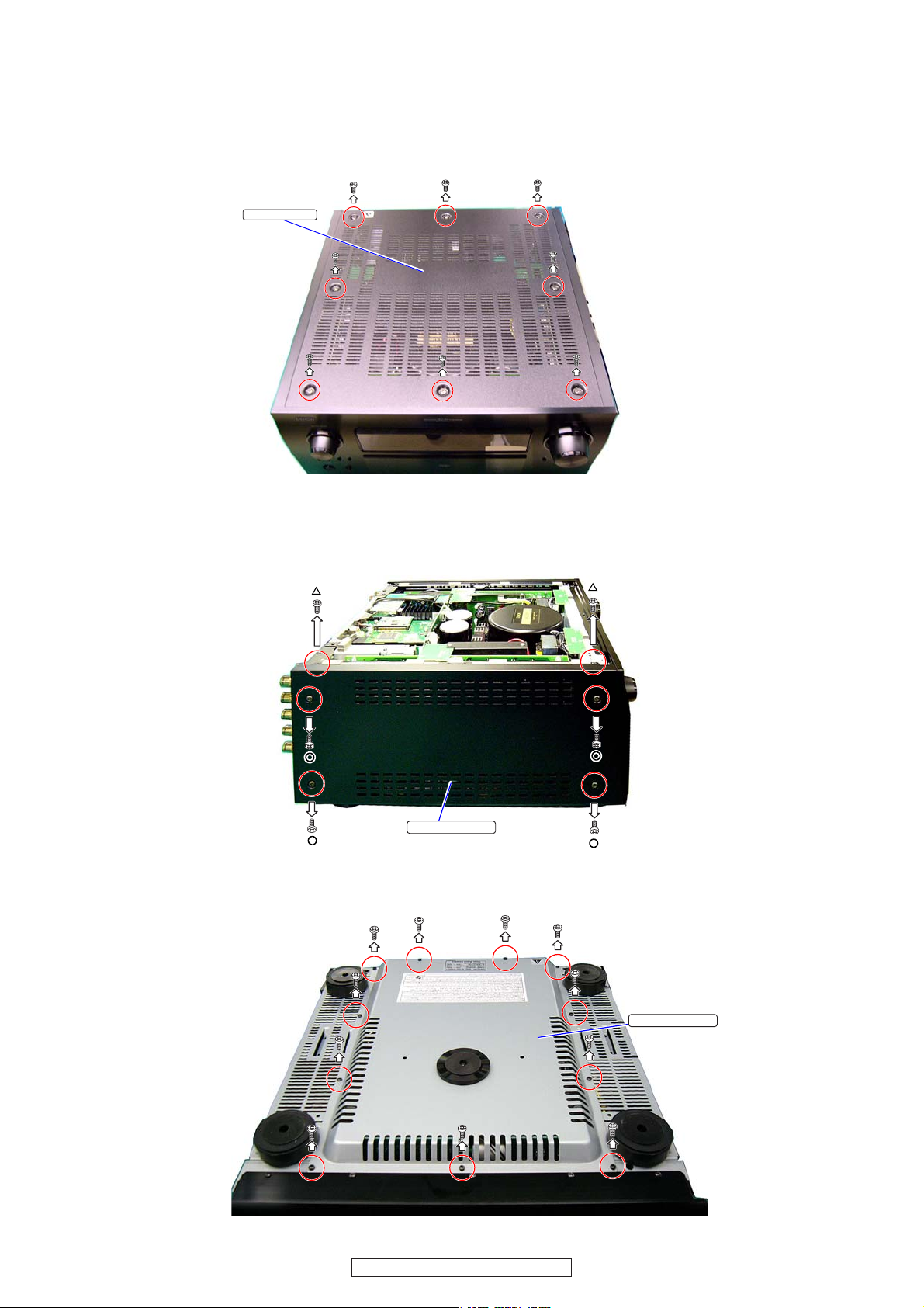
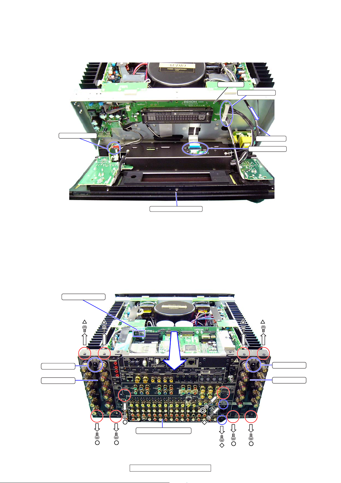
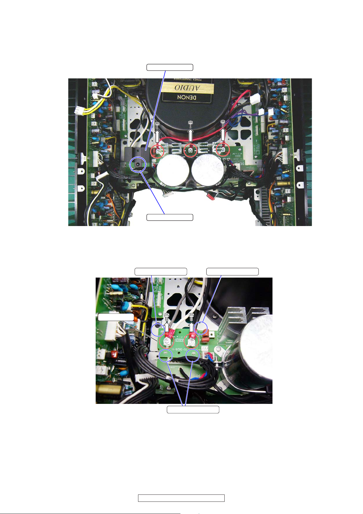
DISASSEMBLY
(Follow the procedure below in reverse order when reassembling.)
1. Top Cover
(1) Remove 8 screws fixing the Top Cover.
TOP COVER
各部のはずしかた
(組み立てるときは、逆の順序で行ってください。)
1. TopCover
(1) ねじを 8 本はずします。
2. Side Cover
(1) Remove 2 screws △ of the top .
(2) Remove 4 screws ○ of the side .
(3) Remove the Side Cover. (Right side is same.)
3. Bottom Cover
(1) Remove 11 screws fixing the Bottom Cover.
2. SideCover
(1) 天面の△ねじを2本はずします。
(2) 側面の○ねじを 4 本はずします。
(3) SIDECOVERをはずします。( 右側も同様。)
SIDE COVER
3. BottomCover
(1) ねじを 11 本はずし Bottomcover を取り外します。
9
AVR-5308CI / AVC-A1HD
BOTTOM COVER
Page 10
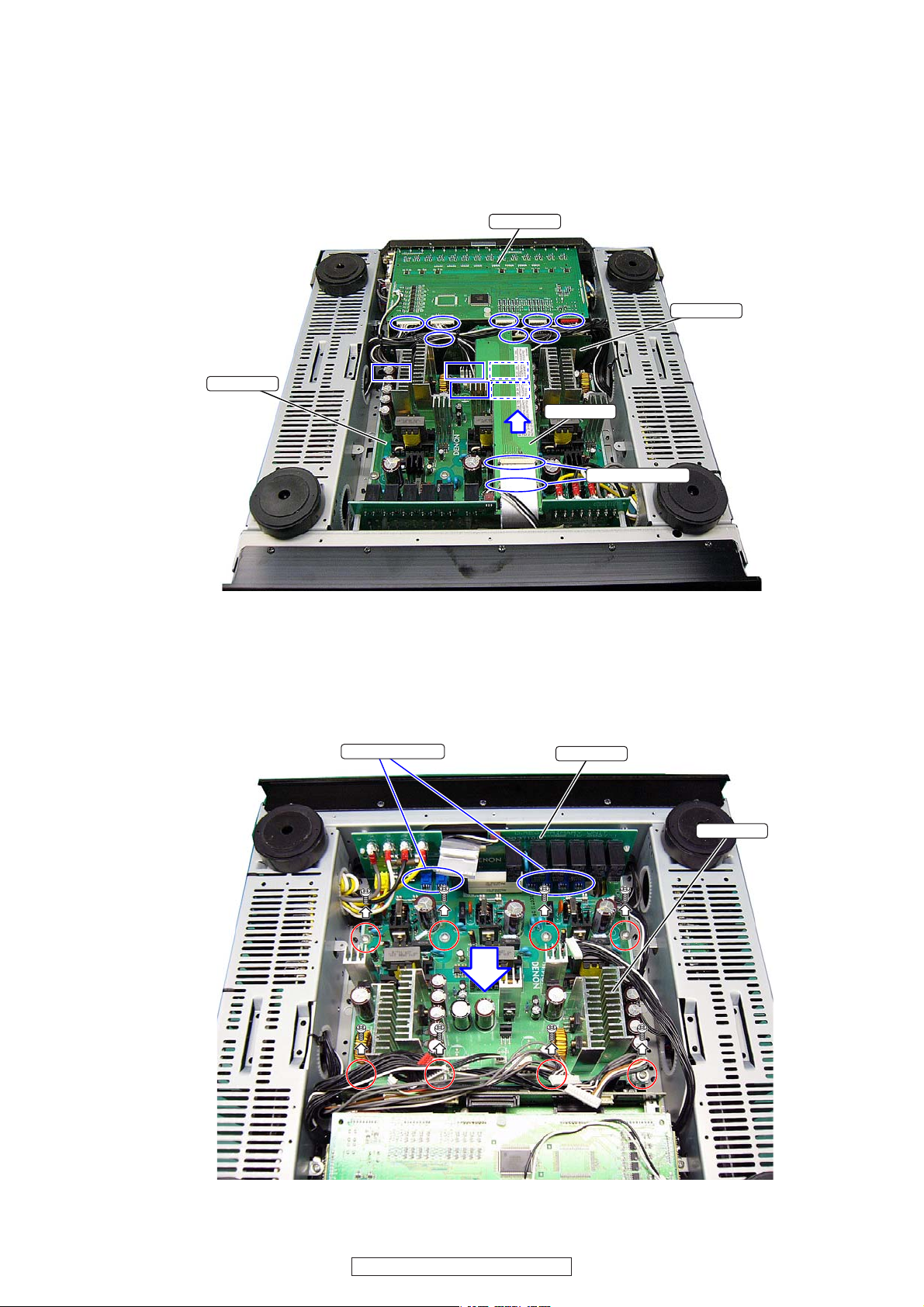
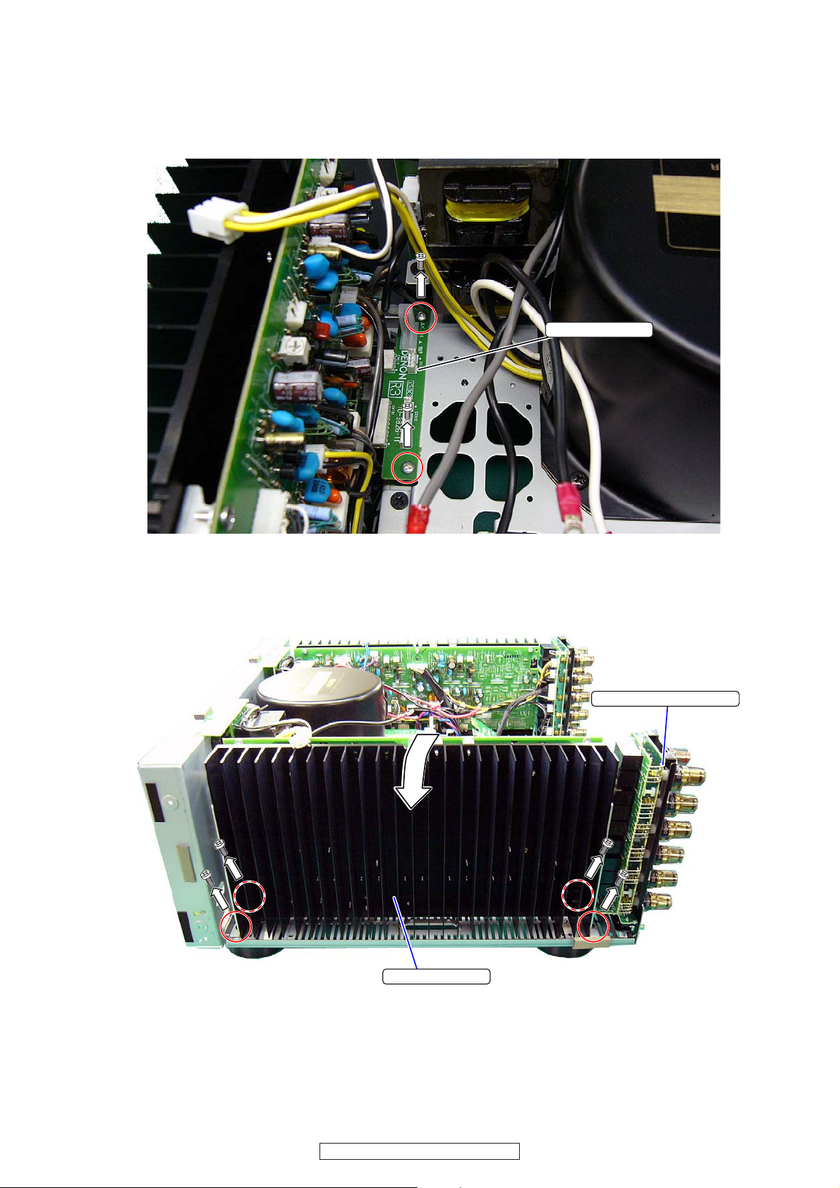
4. 1U-3837 DIGITAL REG. UNIT
(1) Disconnect 5 wires on the 1U-3823-1 : PRE OUT
UNIT and 3 wires on the 1U-3821-1 CPU UNIT.
(2) Disconnect 2 FFC cables. Detach the 1U-3821-2 :
CPU FRONT UNIT.
(3) Disconnect 5 wires on the 1U-3 837-2 : SW REG UNIT.
( □ parts)
1U-3837-2
4. 1U-3837DIGITALREG.UNIT
(1) 1U-3823-1:PREOUTUNITのワイヤー5本 ,1U-3821-
1:CPUUNIT のワイヤー 3 本をはずします。
(2) FFC ケーブル2本をはずし、1U-3821-2:CPUFRONT
UNIT をはずします。
(3) 1U-3837-2:SWREGUNITのワイヤー5本をはずしま
す。(□部分)
1U-3823-1
1U-3821-1
1U-3821-2
FFC Cable
(4) Remove 8 screws fixing the 1U-3837-2 : SW REG
UNIT.
(5) Detach the 1U-3837-2 : SW REG UNIT in the direction
of the arrow. (Board to Board connector for 1U-38371 : PRIMARY UNIT)
Board to Board
(4) 1U-3837-2:SWREGUNIT のねじ 8 本をはずします。
(5) 矢印方向に 1U-3837-2:SWREGUNIT を引き抜きま
す。(1U-3837-1:PRIMARYUNIT との BoardtoBoard
コネクターをはずします。)
1U-3837-1
1U-3837-2
10
AVR-5308CI / AVC-A1HD
Page 11
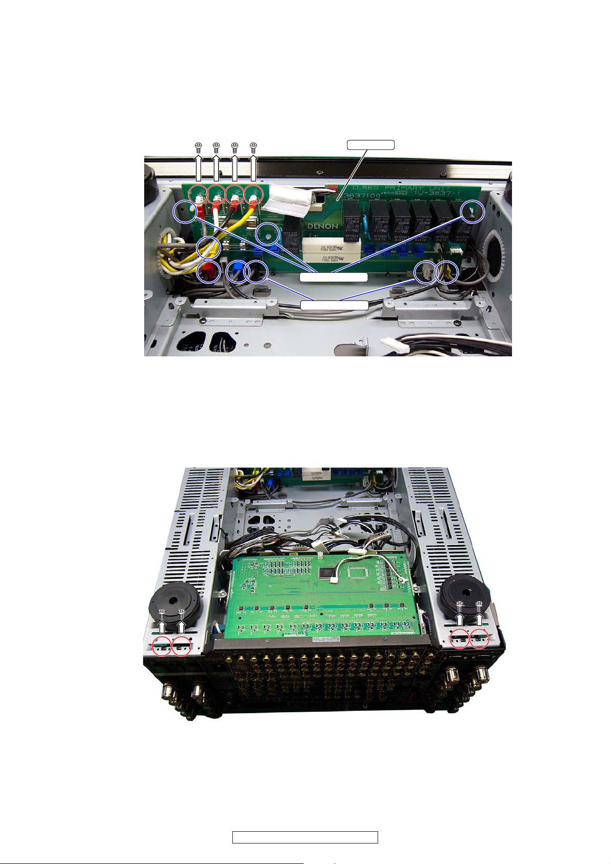
(6) Disconnect 6 VH wire connectors on the 1U-3837-1 :
PRIMARY UNIT.
(7) Remove 4 screws of Powered wire (3T LUG terminal).
(8) Unlock the CARD SPACER. Detach the 1U-3837-1 :
PRIMARY UNIT.
(6) VH ワイヤーを 6ヶ所はずします。
(7) 電源ワイヤー (3T ラグ端子 ) のねじを 4ヶ所はずしま
す。
(8) CARDSPACER のロックをはずし、1U-3837-1:PRI-
MARYUNIT をはずします。
1U-3837-1
CARD SPACER
VH wire
(9) Remove 4 screws fixing the SPEAKER TERMINAL
ASS’Y of bottom side .
(9) SPEAKERTERMINALASS'Y を固定している底面のね
じを 4 本はずします。
(Left side)
11
AVR-5308CI / AVC-A1HD
Page 12
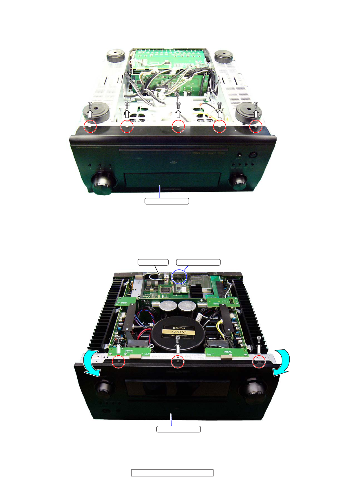
5. FRONT PANEL ASS’Y
(1) Remove 5 screws of bottom side.
5. FRONTPANELASS'Y
(1) 底面のねじを 5 本をはずします。
Front panel
(2) Disconnect the CX530 5P-SHIELD WIRE on the 1U-
3819 : ETHERNET UNIT.
(3) Remove 3 screws of top side.
(4) Tip the Front panel in the direction of the arrow.
1U-3819
(2) 1U-3819:ETHERNETUNITの CX5305P- シールドワ
イヤーをはずします。
(3) 天面のねじを 3 本をはずします。
(4) 矢印の方向にフロントパネルを傾けます。
CX530 5P-wire
Front panel
12
AVR-5308CI / AVC-A1HD
Page 13
(5) Draw the 5P-shield wire in the arrow direction.
(6) Disconnect the CX134,CX802 connector on the 1U-
3825-1 : FLD UNIT.
(7) Disconnect FFC cable.
(8) Disconnect VH connector for Power switch. Detach
the FRONT PANEL Ass’y.
(5) 5P シールドワイヤーを矢印方向に引き出します。
(6) 1U-3825-1:FLDUNIT のコネクター (CX134,CX802)
をはずします。
(7) FFC ケーブルをはずします。
(8) 電源スイッチの VH コネクターをはずして FRONT
PANELAss'y をはずします。
1U-3825-1
CX134,CX802
VH wire
FRONT PANEL Ass'y
6. BACK PANEL ASS’Y
(1) Remove 4 screws △ of top side.
(2) Disconnect the Wire connector.
(3) Remove 2 Push Rivet. Detach the Screw Cover.
(4) Remove screw of the backside of Screw Cover. (Refer
to the following page.)
(5) Remove 6 screws ○ fixing the Back Panel.
(6) Remove 2 screws ◇ fixing the AC INLET.
(7) Draw BACK PANEL Ass’y slowly.
Wire connector
5P-Shield wire
FFC cable
6. BACKPANELASS'Y
(1) △ねじ 4 本をはずします。
(2) WireConnector をはずします。
(3) PushRivet を 2ヶ所はずし、ScrewCover を取り外し
ます。
(4) 次ページを参考に ScrewCover の裏側のねじをはず
します。
(5) ○ねじ 6 本をはずします。
(6) ACINLET の◇ねじ 2 本をはずします。
(7) BACKPANELAss'y をゆっくり引き出します。
Push Rivet
Screw Cover
Push Rivet
Screw Cover
BACK PANEL Ass'y
13
AVR-5308CI / AVC-A1HD
Page 14
The position of the screw of the backside of Screw Cover.
(Right and left remove three screws together.)
ScrewCover の裏側のねじの位置
(左右ともにねじ 3 本をはずします。)
(8) Put up a set aside. Metal holder maintaining AC INLET
go over P.W.B. board.
AC INLET
(9) Disconnect the Wire connector on the 1U-3821-1 :
CPU UNIT.
1U-3821-1
(8) セットを横に立てて ACINLET を保持している金具
が基板の上を通るようにします。
(9) 1U-3821-1:CPUUNIT のワイヤーコネクターをはず
します。
Wire connector
14
AVR-5308CI / AVC-A1HD
Page 15
(10) Pull out Back Panel to lift it halfway.
INSULATING COVER
INSULATING COVER
1U-3828-8
1U-3828-9
(10) BackPanel は途中から持ち上げるように抜き取りま
す。
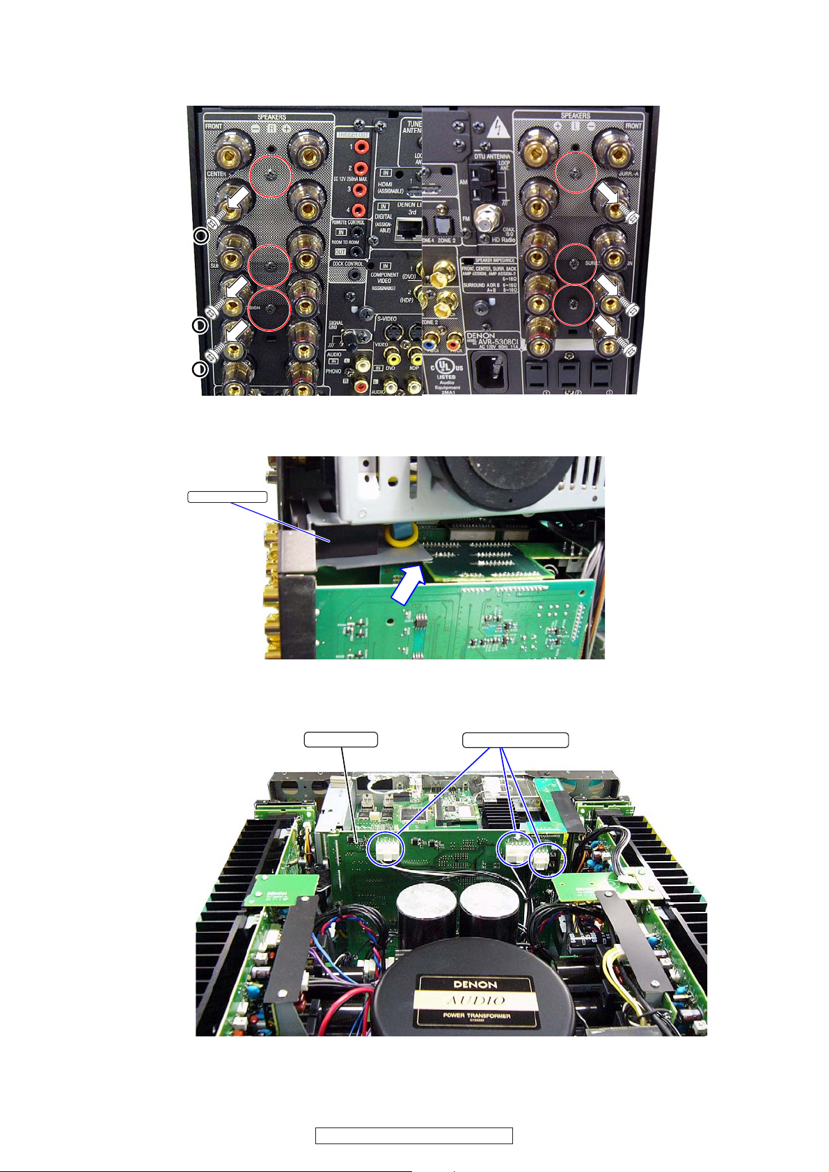
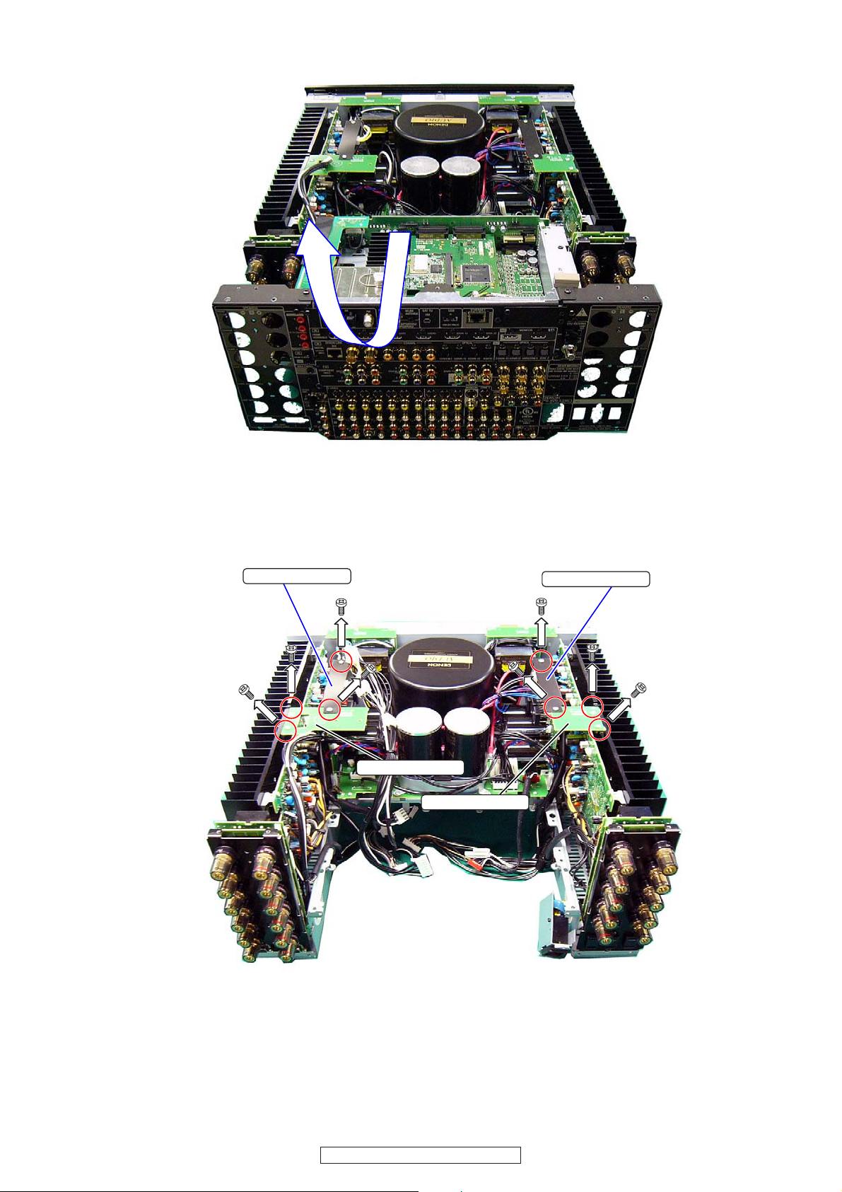
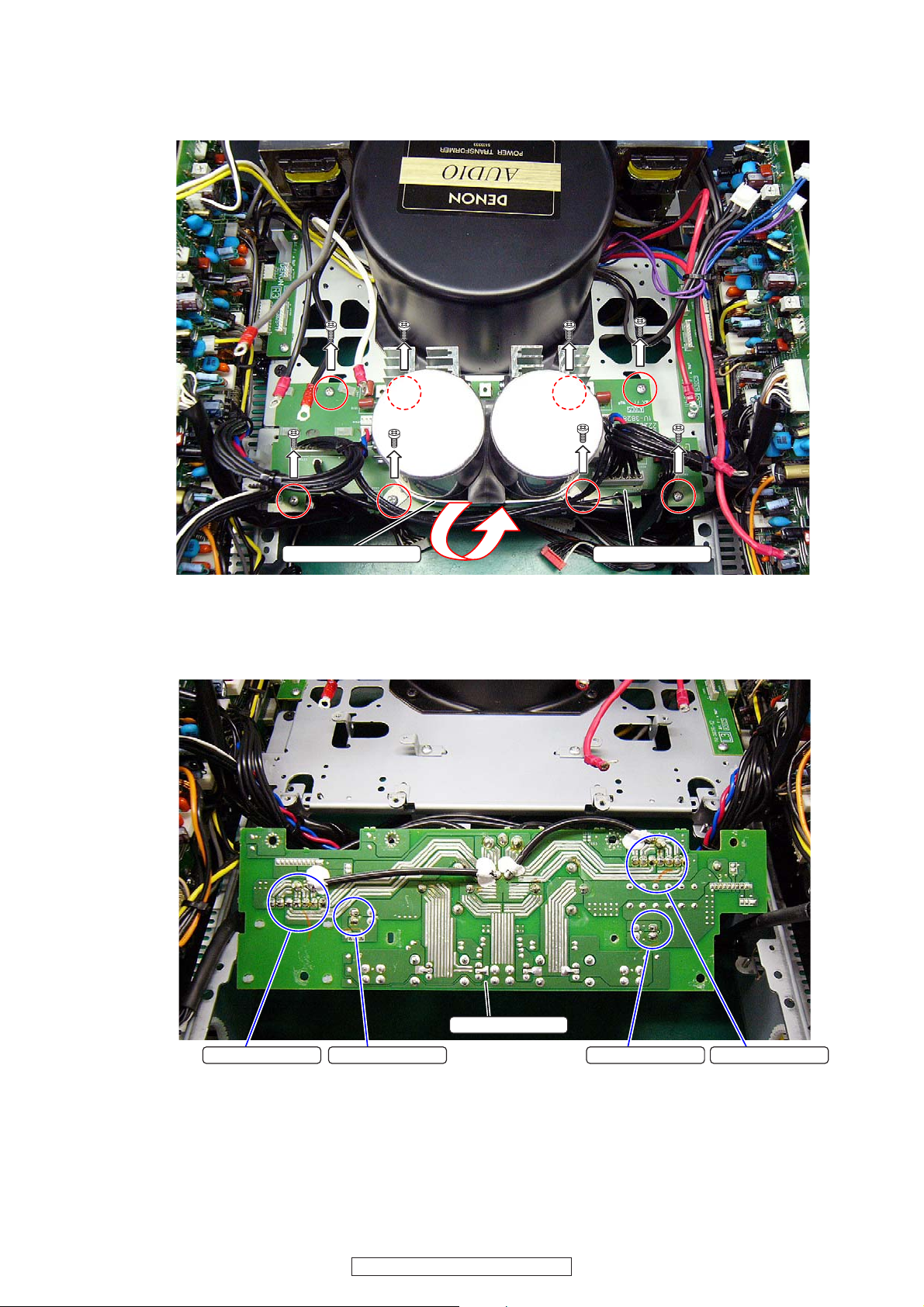
7. AMP (L) UNIT and AMP (R) UNIT
(1) Remove 8 screws. Detach the INSULATING COVER
and 1U-3828-8 :R-SUPPLY JOINT UNIT ,1U-3828-9
:L-SUPPLY JOINT UNIT.
7. AMP(L)UNIT,AMP(R)UNIT
(1) ねじ 8 本をはずして INSULATINGCOVER と接続基板
1U-3828-8:R-SUPPLYJOINTUNIT,1U-3828-9:L-SUP-
PLYJOINTUNIT をはずします。
15
AVR-5308CI / AVC-A1HD
Page 16
(2) Disconnect 4 Wire connectors.
(3) Remove 4 screws. Detach the PWB HOLDER L and
R.
PWB Holder L PWB Holder R
(2) ワイヤーコネクター 4 本をはずします。
(3) ねじ4本をはずして PWBHOLDERL,R を取り外しま
す。
Wire connector
(4) Remove 2 screws.
(5) Detach the 1U-3826-1 : R BLOCKCON UNIT and 1U-
3826-2 : L BLOCKCON UNIT in the direction of the arrow.
Wire connector
(4) ねじ 2 本をはずします。
(5) 1U-3826-1:RBLOCKCONUNIT,1U-3826-2:LBLOCK-
CONUNIT を上に引き抜きます。
1U-3826-1
1U-3826-2
16
AVR-5308CI / AVC-A1HD
Page 17
(6) Remove 3 screws fixing the wire .
(7) Remove Push Rivet. Detach the INSULATING COV-
ER.
INSULATING COVER
(6) ワイヤーを固定しているねじを 3 本はずします。
(7) PushRivet をはずして、INSULATINGCOVER を取り
外します。
Push Rivet
(8) Remove 2 screws fixing the wire .
(9) Unlock the 4 CARD SPACER. Detach the 1U-3828-11
: M3 UNIT.
1U-3828-11
(8) ワイヤーを固定しているねじを 2 本はずします。
(9) CARDSPACERのロックを 4ヶ所はずして、1U-3828-
11:M3UNIT をはずします。
CARD SPACERCARD SPACER
CARD SPACER
17
AVR-5308CI / AVC-A1HD
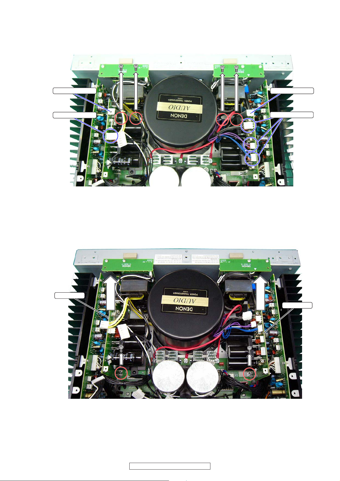
Page 18
(10) Remove 8 screws fixing the 1U-3828-1 : AMP
1U-3828-1
CZ208 CZ732CZ221CZ738
BLOCKCON UNIT and Condenser holder . Reverse
the 1U-3828-1 .
(10) 1U-3828-1:AMPBLOCKCONUNIT とコンデンサーホ
ルダーを固定しているねじ 8 本をはずして基板を裏
返します。
Condenser Holder
(11) I Remove soldering of connec-
tor(CZ738,CZ221,CZ731 and CZ208). Detach the 1U3828-1 : AMP BLOCKCON UNIT.
1U-3828-1
(11) CZ738,CZ221,CZ731,CZ208 の半田をとってはずして
1U-3828-1:AMPBLOCKCONUNIT 基板をはずしま
す。
18
AVR-5308CI / AVC-A1HD
Page 19
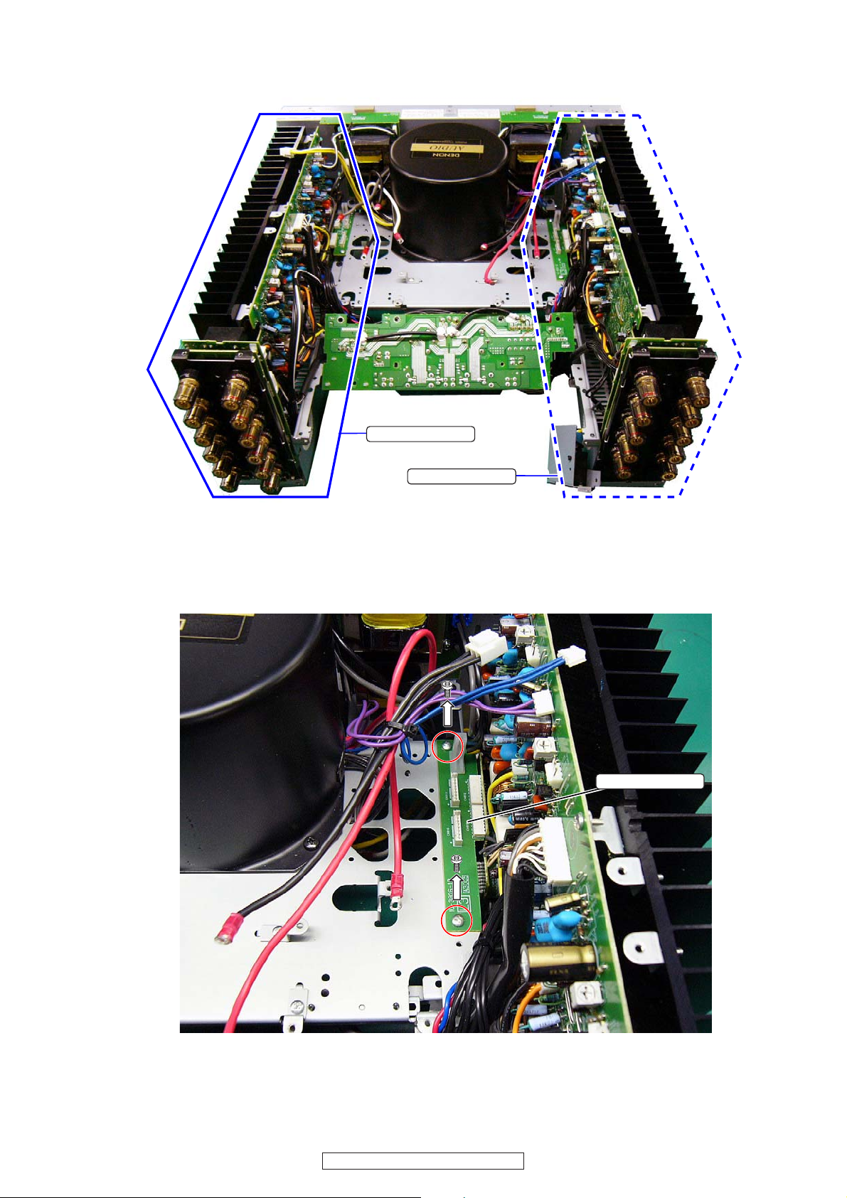
Figure of AMP (L) UNIT/AMP (R) UNIT .
1U-3826-12
AMP(L)UNIT/AMP(R)UNITの形状
AMP(R) UNIT
AMP(L) UNIT
(12) Detach the AMP(L) UNIT.
(12-1) Remove 2 screws fixing the 1U-3826-12 : L
SUPPLY JOINT-3 UNIT. (The board does not yet
come off.)
(12) AMP(L)UNIT をはずします。
(12-1)1U-3826-12:LSUPPLYJOINT-3UNIT を固定して
いるねじ 2 本をはずします。(基板はまだはずれませ
ん。)
19
AVR-5308CI / AVC-A1HD
Page 20
(12-2) Remove 4 screws . Remove RADIATOR UNIT
and SPEAKER TERMINAL UNIT at the same time.
SPEAKER TERMINAL UNIT
(12-2)ねじ 4 本をはずし、RADIATORUNITと
SPEAKERTERMINALUNITを同時に取り外します。
RADIATOR UNIT
(12-3)Detachthe2PWireofACOUTLET.
AC OUTLET
(12-3)ACOUTLETの 2P ワイヤーをはずします。
2P WIRE
20
AVR-5308CI / AVC-A1HD
Page 21
(13) Detach the AMP(R) UNIT.
(13-1) Remove 2 screws fixing the 1U-3826-11 :R
SUPPLY JOINT-1 UNIT.(The board does not yet
come off.)
(13) AMP(R)UNIT をはずします。
(13-1)1U-3826-11:RSUPPLYJOINT-1UNIT を固定し
ているねじ 2 本をはずします。(基板はまだはずれま
せん。)
1U-3826-11
(13-2) Remove 4 screws. Remove RADIATOR UNIT
and SPEAKER TERMINAL UNIT at the same time.
(13-2)ねじ 4 本をはずし、RADIATORUNITと
SPEAKERTERMINALUNITを同時に取り外します。
SPEAKER TERMINAL UNIT
RADIATOR UNIT
21
AVR-5308CI / AVC-A1HD
Page 22
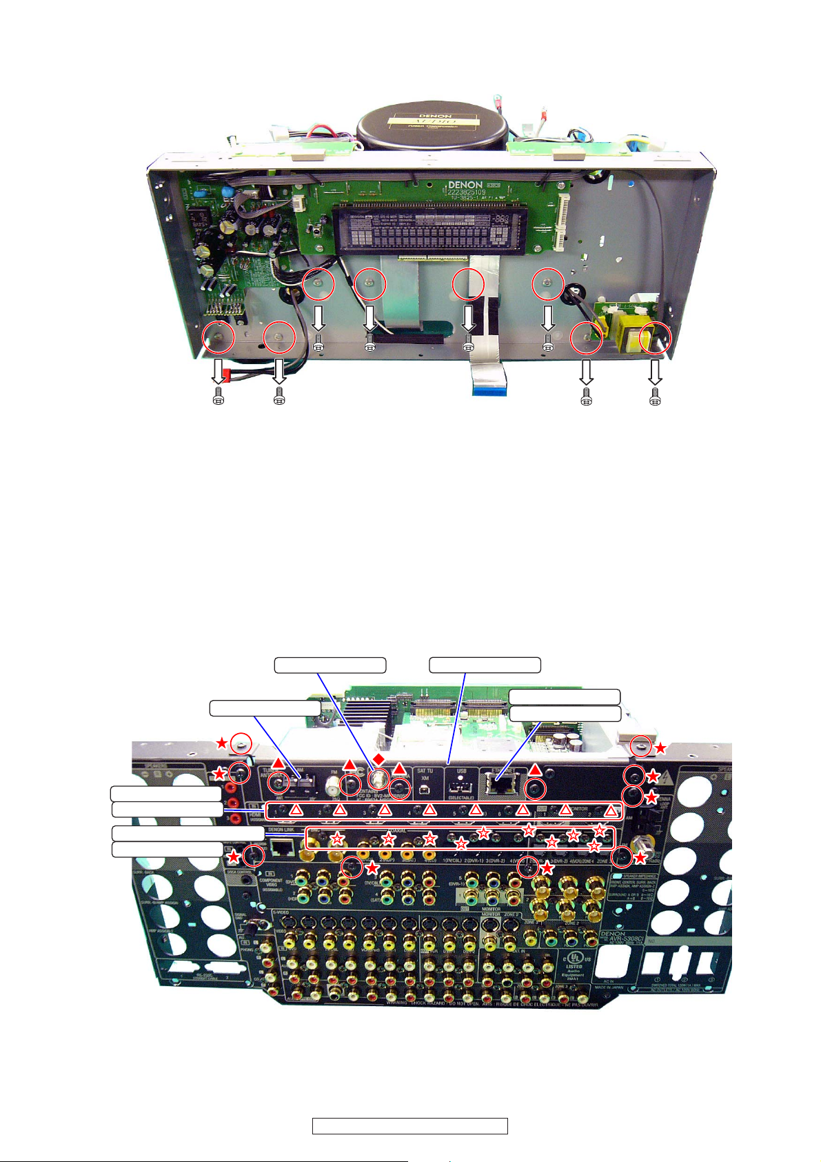
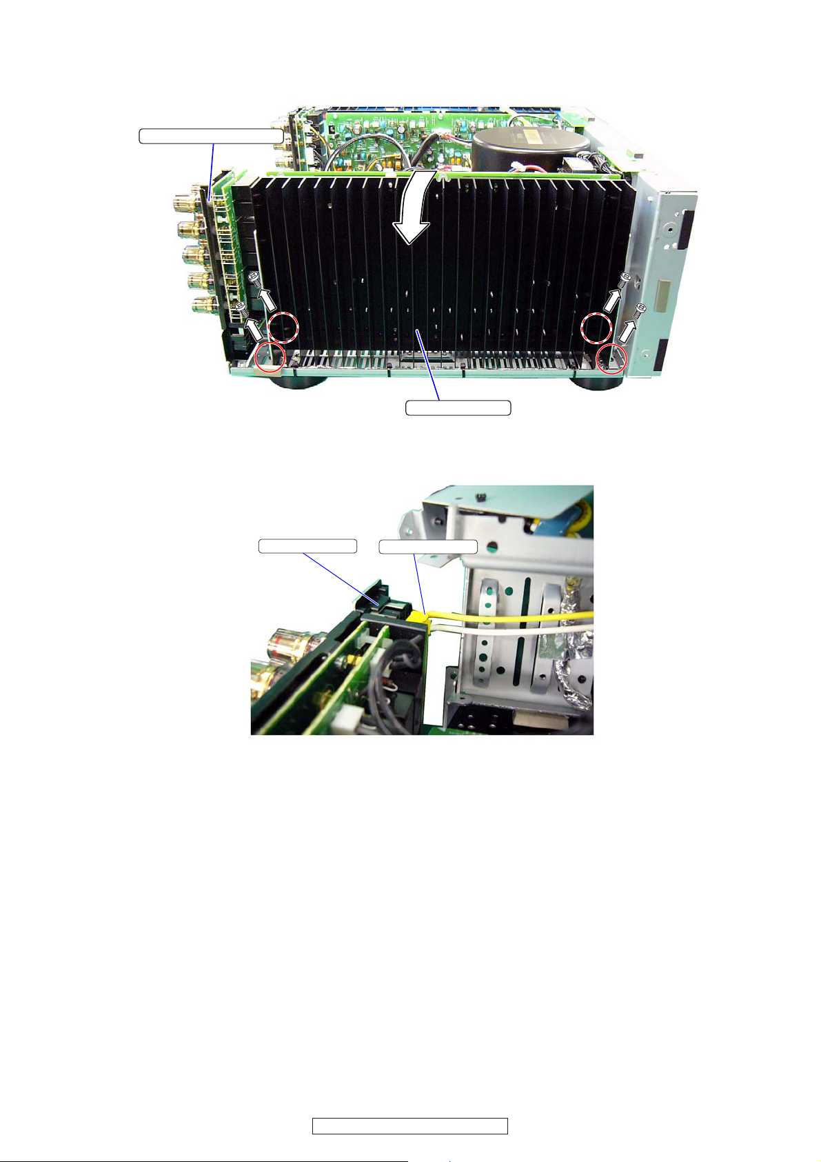
8. FRONT CHASSIS SUB ASS’Y
(1) Remove 8 screws fixing the FRONT CHASSIS.
8. FRONTCHASSISSUBASS'Y
(1) ねじ 8 本をはずし、FRONTCHASSISをはずします。
9. BACK PANEL SUB ASS’Y
(1) Remove 9 screws fixing the REAR PLATE.
(2) Remove 2 screws ▲ fixing the TUNER. Remove 2
screws ▲ fixing the 1U-3819 : ETHERNET UNIT. Re-
move Nut ◆ fixing the WLAN Antenna.
(3) Remove 8 screws △ fixing the HDMI Terminals.
(4) Remove 11 screws ★ fixing the Digital Audio Termi-
nals.
(5) Detach the REAR PLATE.
(6) Pull out the 1U-3819 : ETHERNET UNIT,1U-3833 :
DIGITAL VIDEO UNIT and 1U-3818 : DIGITAL AUDIO
UNIT.
WLAN ANT.
TUNER
1U-3833
HDMI TERMINAL
DIGITAL AUDIO TERMINAL
1U-3818
9. BACKPANELSUBASS'Y
(1) REARPLATEを固定しているねじ 9 本をはずします。
(2) TUNER 固定ねじ▲ 2 本、1U-3819:ETHERNETUNIT
固定ねじ▲ 2 本、WLAN アンテナのナット◆をはず
します。
(3) HDMI 端子のねじ△ 8 本をはずします。
(4) DigitalAudio 端子のねじ★ 11 本をはずします。
(5) REARPLATE をはずします。
(6) 1U-3819:ETHERNETUNIT,1U-3833:DIGITALVIDEO
UNIT,1U-3818:DIGITALAUDIOUNIT 基板を抜き取り
ます。
REAR PLATE
1U-3819
ETHERNET UNIT
22
AVR-5308CI / AVC-A1HD
Page 23
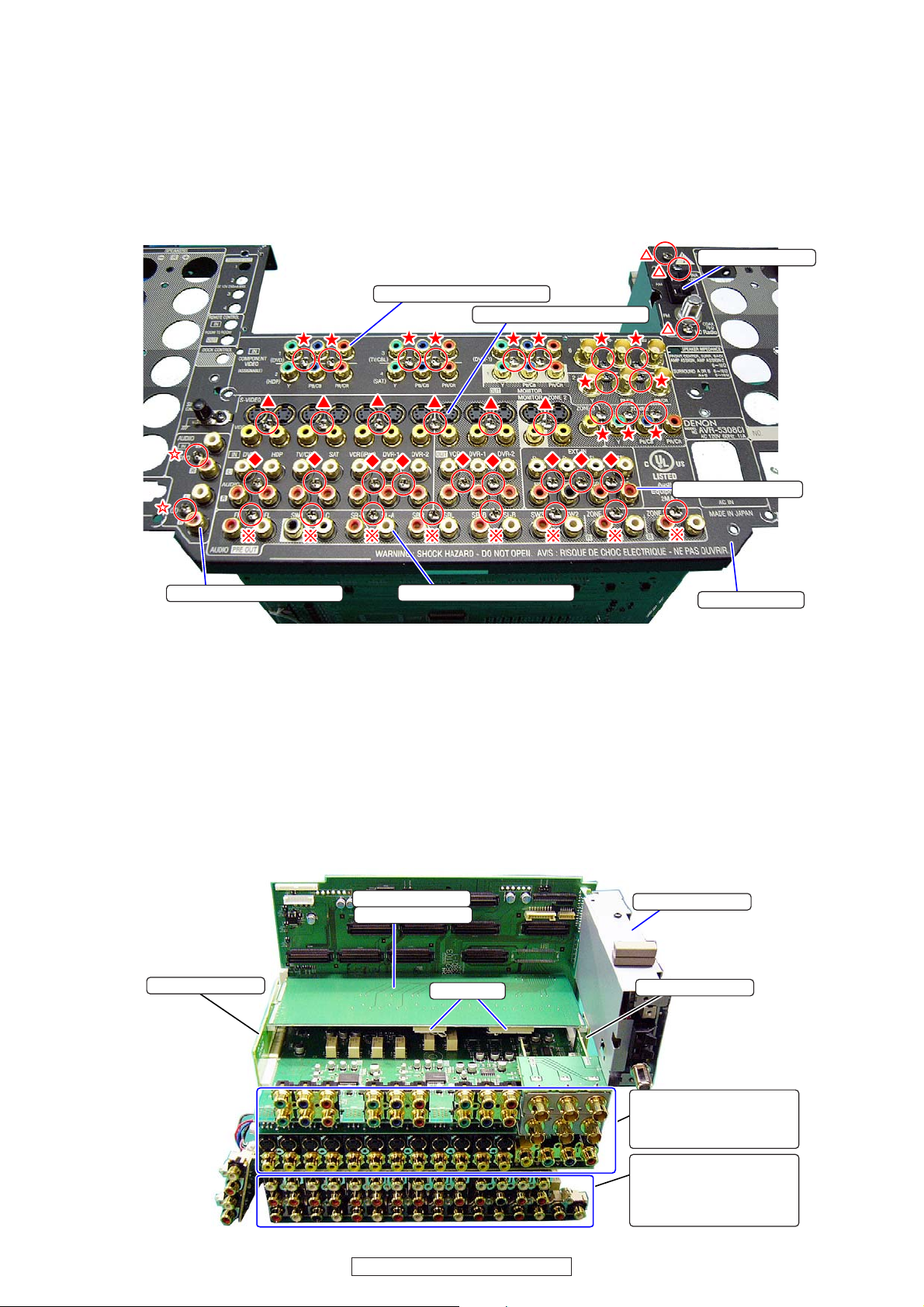
(7) Remove 3 screws △ fixing the HD RADIO.
(8) Remove 13 screws★ fixing the COMPONENT VIDEO
Terminals.
▲
(9) Remove 6 screws
nals.
(10) Remove 9 screws
nals.
(11)Remove 8 screws ※ fixing the PRE OUT Terminals.
(12)Remove 2 screws ☆ fixing the PHONO/CD Terminals.
(13)Detach the BACK PANEL.
fixing the ANALOG VIDEO Termi-
◆
fixing the ANALOG AUDIO Termi-
COMPONENT VIDEO TERMINAL
(7) HDRADIO を固定しているねじ△ 3 本をはずします。
(8) COMPONENTVIDEO端子のねじ★ 13 本をはずしま
す。
(9) ANALOGVIDEO 端子のねじ▲ 6 本をはずします。
(10) ANALOGAUDIO 端子のねじ◆ 9 本をはずします。
(11) PREOUT端子のねじ※ 8 本をはずします。
(12) PHONO/CD 端子のねじ☆ 2 本をはずします。
(13) BACKPANELをはずします。
HD RADIO
VIDEO TERMINAL
AUDIO TERMINAL
PHONO/CD TERMINAL
(14) Detach the HD RADIO UNIT.
(15) Detach the 1U-3821-3 : DAC MUTE UNIT.
(15-1) Detach the 1U-3826-14 and 1U-3826-15.
(15-2) Disconnect 2 Wire connector. Detach the 1U-
3821-3 : DAC MUTE UNIT.
(16) Detach the P.W.B. Ass’y of 1U-3822-1 : COMPO-
NENT UNIT,1U-3822-2 : S&CVBS UNIT and 1U3825-10/-11/-12.
(17)Remove 2 screws of the backside of 1U-3821-1 : CPU
UNIT.
(18) Detach the P.W.B. Ass’y of 1U-3823-1 : PRE OUT
UNIT,1U-3823-2 : AUDIO IN UNIT,1U-3824-1 : VOLUME UNIT and 1U-3824-2 : ZONE VOLUME UNIT.
PRE OUT TERMINAL
1U-3821-3
DAC MUTE UNIT
1U-3826-14
BACK PANEL
(14) HDRADIOUNIT をはずします。
(15) 1U-3821-3:DACMUTEUNIT をはずします。
(15-1)1U-3826-14,1U-3826-15 をはずします。
(15-2)ワイヤー2 本をはずして 1U-3821-3:DACMUTE
UNIT をはずします。
(16) 1U-3822-1:COMPONENTUNIT,1U-3822-2:S&CVBS
UNIT,1U-3825-10/-11/-12 の基板 ASS'Y をはずしま
す。
(17) 1U-3821-1:CPUUNITの裏側のねじ 2 本をはずしま
す。
(18) 1U-3823-1:PREOUTUNIT,1U-3823-2:AUDIOIN
UNIT,1U-3824-1:VOLUMEUNIT,1U-3824-2:ZONE
VOLUMEUNITの基板 ASS'Y をはずします。
HD RADIO UNIT
WIRE
1U-3826-15
23
AVR-5308CI / AVC-A1HD
1U-3822-1 COMPONENT
1U-3822-2 S&CVBS
1U-3825-10/11/12
1U-3823-1 PRE OUT
1U-3823-2 AUDIO
1U-3824-1 VOLUME
1U-3824-2 ZONE.VOLUME
Page 24
●Mattersthatrequireattentionof
the assembling at the time of the
repair.
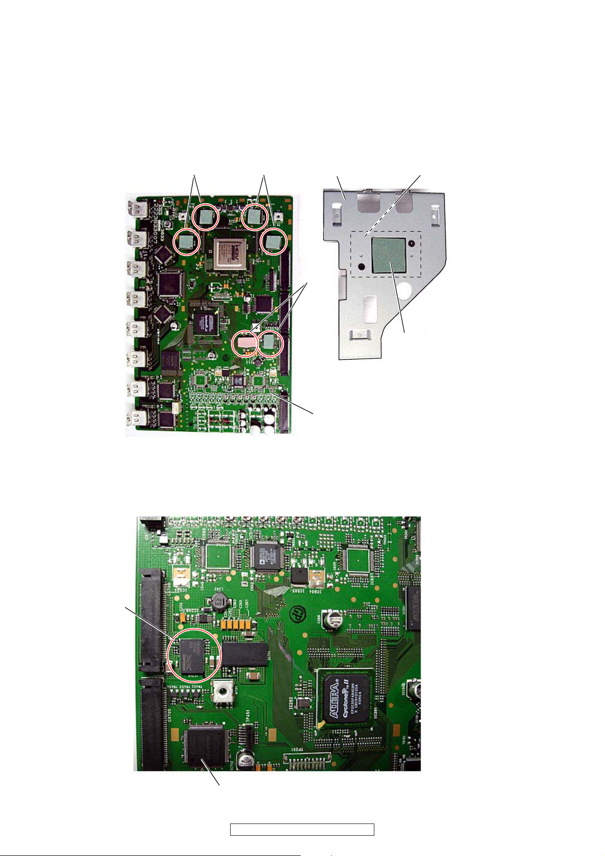
1. Attention when assemble RADIATOR
HOLDER on 1U-3833:DIGITAL VIDEO
UNIT.
(1) Paste up the PAD for heat conduction on the IC and
the RADIATOR.
※ Check nothing is dust on the surface of the PAD.
PADPAD
●修理時の組み立て注意点
1. 1U-3833 : DIGITAL VIDEO 基板に RADI-
ATOR HOLDER を取り付ける時の注意
(1) IC と RADIATOR に熱伝導用 PAD が貼ってあること。
※ PAD の表面に異物の付着が無いこと。
RADIATOR HOLDER
PAD
RADIATOR
PAD
(2) Check nothing is chink between the PAD and the
parts, after attach the RADIATOR HOLDER to the 1U3833 :DIGITAL VIDEO UNIT.
(3) It is a regular state that is short-circuited No.30 pin and
GND (No.29 or No.31 pin) of the IC710 on the 1U3833:DIGITAL VIDEO UNIT .
IC710
1U-3833
DIGITAL VIDEO UNIT
(2) 1U-3833:DIGITALVIDEO 基板に RADIATORHOLDER
を取り付けた後に PAD と部品に隙間がないか確認の
こと。
(3) 1U-3833:DIGITALVIDEO 基板:IC710 の No.30 ピン
と GND(No.29 または No.31 ピン ) が短絡されている
のは正規な状態です。
1U-3833
DIGITAL VIDEO UNIT
24
AVR-5308CI / AVC-A1HD
Page 25
2. Attention when assemble 1U3818:DIGITAL AUDIO UNIT and 1U3833:DIGITAL VIDEO UNIT on 1U-38211:CPU UNIT.
(1) Hold the 1U-3821-1:CPU UNIT so that the connector
CX713 on the 1U-3821-3:DAC MUTE UNIT is unstable. Then connect the 1U-3818:DIGITAL AUDIO UNIT
and the 1U-3833:DIGITAL VIDEO UNIT to connector.
2. 1U-3818:DIGITALAUDIO 基板と 1U3833:DIGITALVIDEO基板を 1U-3821-1
:CPU基板に取り付ける時の注意
(1) 1U-3821-3:DACMUTE 基板のコネクター CX713 に
浮きが発生しないように 1U-3821-1:CPU基板を押
えながら 1U-3818:DIGITALAUDIO 基板と 1U-3833:
DIGITALVIDEO 基板をコネクターに差し込んでくだ
さい。
1U-3821-3
DAC MUTE UNIT
HOLD
DIGITAL VIDEO UNIT
1U-3818
DIGITAL AUDIO UNIT
1U-3821-1
CPU UNIT
CX713
1U-3833
25
AVR-5308CI / AVC-A1HD
Page 26
CHECK WITH TEST MODE
µcom/DSP Error Display Mode
1. Operation Spec
µcom version display mode:
When the following conditions are satisfied at its starting state, error information is displayed before version information.
Starting method (same as µcom version display):
While pressing 2 buttons, "STATUS " and "MONITOR SELECT ", turn on Power switch.
Then, press "STATUS" button to display the following information on the FL Display.
2. Display Order
Error information →Destination information →Main-µcom version information → Sub-µcom version information
→ DSP version information
3. Display
Any one of the following list is displayed, in the priority of qwerty..
Condition State Display
Sub-µcom NG
q
w DIR NG
e DSP1 NG
r DSP2 NG
t DSP3 NG
y
Both SUB/DSP
OK
No response from Sub-µcom
No response from DIR
When DSP boot, executing DSP reset makes no change to BUSY port "L".
No change to BUSY port "L" before issuing DSP command.
When DSP data read, executing WRITE="L" makes no change to ACK="H".
When DSP data read, executing REQ="L" makes no change to ACK="L".
When DSP data write, executing WRITE="H" makes no change to ACK="H".
When DSP data write, executing REQ="L" makes no change to ACK="L".
When DSP special code boot, executing DSP reset makes no change to
BUSY port "L".
No change to BUSY port "L" before issuing DSP special read command.
No change to BUSY port "L" before DSP version read.
" □ SUB □□ ERROR □01□ "
" □ DIR □□ ERROR □01□ "
"□DSP1 □ ERROR □01□ "
"□DSP1 □ ERROR □02□ "
"□DSP1 □ ERROR □03□ "
"□DSP1 □ ERROR □04□ "
"□DSP1 □ ERROR □05□ "
"□DSP1 □ ERROR □06□ "
"□DSP1 □ ERROR □11□ "
"□DSP1 □ ERROR □12□ "
"□DSP1 □ ERROR □13□ "
"□DSP2 □ ERROR □01□ "
"□DSP2 □ ERROR □02□ "
"□DSP2 □ ERROR □03□ "
"□DSP2 □ ERROR □04□ "
"□DSP2 □ ERROR □05□ "
"□DSP2 □ ERROR □06□ "
"□DSP2 □ ERROR □11□ "
"□DSP2 □ ERROR □12□ "
"□DSP2 □ ERROR □13□ "
"□DSP3 □ ERROR □01□ "
"□DSP3 □ ERROR □02□ "
"□DSP3 □ ERROR □03□ "
"□DSP3 □ ERROR □04□ "
"□DSP3 □ ERROR □05□ "
"□DSP3 □ ERROR □06□ "
"□DSP3 □ ERROR □11□ "
"□DSP3 □ ERROR □12□ "
"□DSP3 □ ERROR □13□ "
(No error display, version display only)
26
AVR-5308CI / AVC-A1HD
Page 27
テストモードによるチェック方法
マイコン・DSP エラー表示モード
1. 動作仕様
マイコンバージョン表示モード :
起動状態にて下記の条件に該当した場合は、バージョン情報表示の前にエラー情報を表示します。
起動方法 ( マイコンバージョン表示と同様 ):
"STATUS","MONITORSELECT" の 2 つのボタンを押した状態で、電源スイッチを押して電源を入れます。
その後、"STATUS" ボタンを押すと下表の内容が FLDisplay に表示されます。
2. 表示順序
エラー情報→仕向地表示→メインマイコンバージョン情報→サブマイコンバージョン情報
→DSP バージョン情報
3. 表示条件
下表のいずれかを表示します。表示の優先順は、qwerty。
条件 状態 表示内容
q
SUB
マイコンが
wDIR が NG
eDSP 1がNG
rDSP 2がNG
tDSP 3がNG
ySUB/DSP 共に
OK
NG
SUB マイコンからの応答がない
DIR からの応答がない
DSP コードブート時、DSP リセットを実行しても BUSY ポートが "L" にならない
DSP コマンド発行前に、BUSY ポートが "L" にならない " □ DSP1 □ ERROR □02□ "
DSP データリード時、WRITE="L" としても ACK="H" とならない " □ DSP1 □ ERROR □03□ "
DSP データリード時、REQ="L" としても ACK="L" とならない " □ DSP1 □ ERROR □04□ "
DSP データライト時、WRITE="H" としても ACK="H" とならない " □ DSP1 □ ERROR □05□ "
DSP データライト時、REQ="L" としても ACK="L" とにならない " □ DSP1 □ ERROR □06□ "
DSP スペシャルコードブート時、DSP リセットを実行しても
BUSY ポートが "L" にならない
DSP スペシャルリードコマンド発行前に、BUSY ポートが "L" にならない " □ DSP1 □ ERROR □12□ "
DSP バージョンリード前に、BUSY ポートが "L" にならない " □ DSP1 □ ERROR □13□ "
DSP コードブート時、DSP リセットを実行しても BUSY ポートが "L" にならない
DSP コマンド発行前に、BUSY ポートが "L" にならない " □ DSP2 □ ERROR □02□ "
DSP データリード時、WRITE="L" としても ACK="H" とならない " □ DSP2 □ ERROR □03□ "
DSP データリード時、REQ="L" としても ACK="L" とならない " □ DSP2 □ ERROR □04□ "
DSP データライト時、WRITE="H" としても ACK="H" とならない " □ DSP2 □ ERROR □05□ "
DSP データライト時、REQ="L" としても ACK="L" とにならない " □ DSP2 □ ERROR □06□ "
DSP スペシャルコードブート時、DSP リセットを実行しても
BUSY ポートが "L" にならない
DSP スペシャルリードコマンド発行前に、BUSY ポートが "L" にならない " □ DSP2 □ ERROR □12□ "
DSP バージョンリード前に、BUSY ポートが "L" にならない " □ DSP2 □ ERROR □13□ "
DSP コードブート時、DSP リセットを実行しても BUSY ポートが "L" にならない
DSP コマンド発行前に、BUSY ポートが "L" にならない " □ DSP3 □ ERROR □02□ "
DSP データリード時、WRITE="L" としても ACK="H" とならない " □ DSP3 □ ERROR □03□ "
DSP データリード時、REQ="L" としても ACK="L" とならない " □ DSP3 □ ERROR □04□ "
DSP データライト時、WRITE="H" としても ACK="H" とならない " □ DSP3 □ ERROR □05□ "
DSP データライト時、REQ="L" としても ACK="L" とにならない " □ DSP3 □ ERROR □06□ "
DSP スペシャルコードブート時、DSP リセットを実行しても
BUSY ポートが "L" にならない
DSP スペシャルリードコマンド発行前に、BUSY ポートが "L" にならない " □ DSP3 □ ERROR □12□ "
DSP バージョンリード前に、BUSY ポートが "L" にならない " □ DSP3 □ ERROR □13□ "
"□SUB□ □ ERROR □01□ "
"□DIR□ □ ERROR □01□ "
" □ DSP1 □ ERROR □01□ "
" □ DSP1 □ ERROR □11□ "
" □ DSP2 □ ERROR □01□ "
" □ DSP2 □ ERROR □11□ "
" □ DSP3 □ ERROR □01□ "
" □ DSP3 □ ERROR □11□ "
( 表示せずにバージョン表示を行う )
27
AVR-5308CI / AVC-A1HD
Page 28

ADJUSTMENT
調整
AUDIO Section
IDLING CURRENT (1U-3827-1,6)
Required measurement equipment: DC Voltmeter
1. PREPARATION
(1) Avoid direct blow from an air conditioner or an electric
fan, and adjust the unit at normal room temperature 15
°C ~ 30 °C (59 °F ~ 86 °F).
(2) Presetting
• POWER (Power source switch) OFF
• SPEAKER (Speaker terminal) No load
(Do not connect speaker, dummy resistor, etc.)
2. ADJUSTMENT
(1 ) Remove Top co ver .
Set VR201,203,204 on 1U-3827-1 : P.AMP(L) Unit
and VR401,402,403,404 on 1U-3827-6 : P.AMP(R)
Unit at fully counterclockwise (
(2) Connect DC Voltmeter to test points (q epin of
TP201,202,203 and TP401,402,403,404).
(3) Connect power cord to AC Line, and turn power switch
"ON".
(4) Turn power switch "ON" with pressing [STANDARD]
and [HOME THX CINEMA] buttons in the door of front
panel.
(5) Presetting.
・MASTER VOLUME :
・SPEAKER (Speaker terminal) : No load
(Do not connect speaker, dummy resistor, etc.)
MODE : 9CH STEREO
FUNCTION : CD
(6) Allow 2 minutes, and turn VR201 clockwise (
adjust the TEST POINT voltage to
3.5 mV ± 0.2 mV DC.
(7) After 10 minutes from preset, turn VR201 to set the
voltage to
4.0 mV ± 0.2 mV DC.
(8) Adjust the Variable Resistors of other channels in the
same way.
c ).
"---" counterclockwise (
cmin.)
x ) to
オーディオセクション
アイドリング電流の調整 (1U-3827-1,6)
調整に必要な測定器 : DCVoltmeter
1. 準備
(1) セットをクーラ、扇風機のそばなど風通しの良い場
所を避け、通常の使用状態に置きます。セットの周
囲温度は 15〜30 ℃、湿度は常湿とします。
(2) プリセット
・電源スイッチ OFF
・スピーカー端子 無負荷
( スピーカー・ダミー抵抗器などを接続しない。)
2. 調整
(1) トップカバーをはずし、1U-3827-1:P.AMP(L) ユニッ
トの VR201,203,204 と 1U-3827-6:P.AMP(R) ユニッ
トの VR401,402,403,404 を反時計方向 (
切った状態にセットします。
(2) テストポイント (TP201,202,203 と
TP401,402,403,404 の q epin)に DCVoltmeterを接
続します。
(3) 電源コードを AC ライン(95〜105Vの範囲であるこ
と)に接続し、電源スイッチを "ON"にします。
(4) フロントパネルのドア内にある「STANDARD」ボタ
ンと「HOMETHXCINEMA」ボタンを押しながら電
源スイッチを "ON"にします。
(5) ON後、次のようにセットします。
・MASTERVOLUME(音量調節つまみ)→反時計方向
(
c)に回す、最小の状態にする。
・SPEAKER(スピーカー端子)→無負荷
(スピーカー、ダミー抵抗器などを接続しない。)
MODE:9CHSTEREO
FUNCTION:CD
(6) 2分以内に VR201を時計方向 (
イントの電圧を次のように調整します。
3.5mV ±0.2mVDC
(7) 予備調整から 10分後 VR201を回し、次のように電
圧を設定します。
4.0mV± 0.2mVDC
(8) 同じ方法で各チャネルの可変抵抗を調整します。
x) に回しテストポ
c)に回し
(9) After 5 minutes from (7), turn VR201 to set the voltage
to
4.0 m ± 0.2 mV DC.
(10)Adjust the Variable Resistors of other channels in the
same way.
AVR-5308CI / AVC-A1HD
(9) (7) 項設定から 5分後 VR201を回し、次のように電
圧を設定します。
4.0mV± 0.2mVDC
(10) 同じ方法で各チャネルの可変抵抗を調整します。
28
Page 29
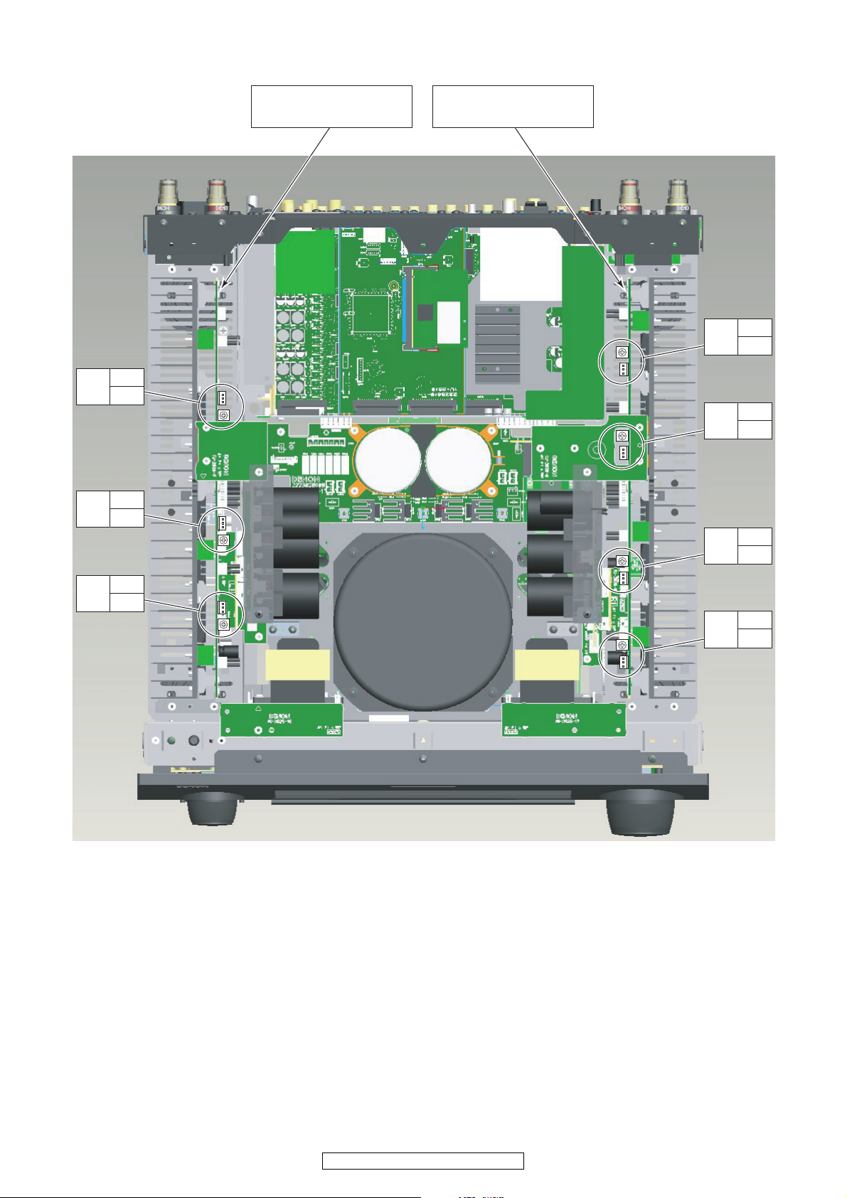
Position of Test point and Adjustment volume.
テストポイントと調整ボリュームの位置
FL
SL
TP203
VR204
TP202
VR203
P.AMP(L) UNIT
P.AMP(R) UNIT
1U-3827-1 1U-3827-6
C
FR
SR
VR401
TP401
VR403
TP402
VR404
TP403
SBL
TP201
VR201
SBR
VR402
TP404
29
AVR-5308CI / AVC-A1HD
Page 30

VIDEO Section
. MAIN ZONE
I
1. SETTING
(1) Connect the oscilloscope to the Y-signal and C-signal
of S MONITOR OUT terminal and each terminate at
75 Ohms.
(2) Connect the oscilloscope to the Y-signal, P
B-signal, PR-signal and CR-signal of COMPO-
and C
NENT MONITOR OUT2 terminal and each terminate
at 75 Ohms.
※ Use the 75 Ohms resistance must be 1%
(3) DVD test disc : DVDT-S01 or VT-502
(4) COMPONENT VIDEO OUT of DVD player is connect-
ed to COMPONENT IN-5.
2. BEFORE ADJUSTMENT
2.1. Setting the Oscilloscope as below.
(1) PB/CB, PR/CR, C
(a) TIME/DIV : 10μs
(b) VOLT/DIV : 100mV (Use the probe : x10 )
(2) Y
(a) TIME/DIV : 10μs
(b) VOLT/DIV : 200mV (Use the probe : x10 )
Power on. Power Supply : 120V(U.S.A.)
230V(Europe)
100V(Japan)
2.2. Setup the DVD player and confirmation of the stators
(1) Set to "INTERLACED" mode at the COMPONENT
OUT.
(2) Confirm the DVD player’s out put level is equal as the
item 2.4. in following.
2.3. Preparation
(1) Connect power cord to AC Line, and turn power switch
"ON".
(2) Turn the FUNCTION knob to select "VCR/iPOD" input.
(3) Push [OPEN/CLOSE] button of DVD player, then
open the Disc Tray.
Set DVD test disc on the Disc Tray, and then push
[CLOSE] button.
(4) DVD player FL display appear "STOP", push [PLAY]
button to playback DVD.
(5) Push the [DISPLAY] button of remote control of DVD
player unit and then appear the ON-Screen Display
(GUI) on the monitor TV.
(6) [DVD test disc : DVDT-S01]
P u s h t h e [ + 1 0 ] a n d [ 2 ] b u t t o n , s e l e c t T i t l e 1 2 o f D V D .
[DVD test disc : VT-502]
Push the [0] and [3] button, select Title 3 of DVD.
(7) [DVD test disc : DVDT-S01]
Push the [ENTER] button, playback Title 12.
(color bar 75%)
[DVD test disc : VT-502]
Push the [ENTER] button, playback Title 3.
(color bar 100%)
B-signal
ビデオセクション
I.MAINZONE
1. セッティング手順
(1) セットの SMONITOROUT 端子から Y 信号と C 信号
をそれぞれオシロスコープ(終端抵抗:75Ω)に接
続します。
(2) セットの COMPONENTMONITOROUT2 の端子(Y,
B/CB,PR/CR)をそれぞれオシロスコープ(終端抵
P
抗:75Ω)に接続します。
※ 75Ω 抵抗は 1%品を使用する事。
(3) DVD テストディスク:DVDT-S01 または VT-502 を
用意します。
(4) DVD プレーヤーの COMPONENTVIDEOOUT を
COMPONENTIN-5 に接続します。
2. 調整のまえに
2.1. オシロスコープを下記に設定
(1) PB/CB,PR/CR,C
(a) TIME/DIV : 10μs
(b) VOLT/DIV : 100mV(プローブ x10 使用)
(2) Y
(a) TIME/DIV : 10μs
(b) VOLT/DIV : 200mV(プローブ x10 使用)
電源電圧:100V(日本)
2.2. DVD プレーヤの設定と確認
(1) COMPONENTOUT の設定を " インターレース " にしま
す。
(2) DVD プレーヤーの出力が以下 2.4. に合っていること
を確認します。
2.3. 準備手順
(1) 電源コードを AC ラインに接続し、電源スイッチを
"ON"にします。
(2) FUNCTION ノブを回し、入力を "VCR/iPOD" に切り替
えます。
(3) DVD プレーヤーの「OPEN/CLOSE」ボタンを押しト
レイを開き、トレイ上に DVD テストディスクをセッ
ト後、「CLOSE」ボタンを押します。
(4) DVD プレーヤーの表示管上に "STOP" が表示されて
から、「PLAY」ボタンを押し、ディスクを再生しま
す。
(5) DVD プレーヤーのリモコンの「DISPLAY」ボタンを
押しグラフィカル・ユーザー・インターフェイス
(GUI) 画面を出します。
(6) [DVD テストディスク:DVDT-S01 の場合]番号ボタ
ンの「 +10 」 , 「 2 」ボタンを押し、Title12 を選択しま
す。 [DVD テストディスク:VT-502 の場合]番
号ボタンの「0 」, 「 3 」ボタンを押し、Title3 を選択しま
す。
(7) [DVD テストディスク:DVDT-S01 の場合]
「ENTER」ボタンを押し、Title12 を再生します。
(75%カラーバー信号)
[DVD テストディスク:VT-502 の場合]
「ENTER」ボタンを押し、Title3 を再生します。
(100%カラーバー信号)
30
AVR-5308CI / AVC-A1HD
Page 31

2.4. Procedure
(1) Adjust the signal of S MONITOR OUT by the wave of
oscilloscope.
(a) Target, Y-signal
Point : 1U-3833-1 VR504
Adjustment Value : 714 ± 14mV
Waveform
2.4. 手順
(1) セットの SMONITOROUT の信号レベルをオシロス
コープ上の波高値で調整します。
(a) Y 信号レベル
調整個所 : 1U-3833-1VR504
調整値 : 714 ± 14mV
波形
Y
Y-signal of S MONITOR OUT
(b) Target, C-signal
Point : 1U-3833-1 VR505
Adjustment Value : 286 ± 5mV
Waveform
C
C-signal of S-MONITOR
(2) Adjust the signal of COMPONENT OUT by the wave
of oscilloscope.
(a) Target, Y-signal
Point : 1U-3833-1 VR506
Adjustment Value : 714 ± 14mV
Waveform
Y
SMONITOROUT の Y 信号レベル
(b) C 信号レベル
調整個所 : 1U-3833-1VR505
調整値 : 286 ± 5mV
波形
C
SMONITOR の C 信号レベル
(2) COMPONENTOUTの信号レベルをオシロスコープ上
の波高値で調整します。
(a) Y 信号レベル
調整個所 : 1U-3833-1VR506
調整値 : 714 ± 14mV
波形
Y
Y-signal COMPONENT OUT
(b) Target, P
Point : 1U-3833-1 VR507
Adjustment Value :
*700 ± 14mV (VT-502)
Waveform
B/CB-signal
*525 ±10mV (DVDT-S01)
PB/CB
PB/CB-signal COMPONENT OUT
AVR-5308CI / AVC-A1HD
31
Y
COMPONENTOUT の Y 信号レベル
B/CB 信号レベル
(b) P
調整個所 : 1U-3833-1VR507
調整値 : 525 ± 10mV(DVDT-S01)
700 ± 14mV(VT-502)
波形
PB/CB
COMPONENTOUT の PB/CB 信号レベル
Page 32

(c) Target, PR/CR-signal
Point : 1U-3833-1 VR508
Adjustment Value : *525 ±10mV (DVDT-S01)
*700 ± 14mV (VT-502)
Waveform
(c) PR/CR 信号レベル
調整個所 : 1U-3833-1VR508
調整値 : 525 ± 10mV(DVDT-S01)
700 ± 14mV(VT-502)
波形
PR/CR
PR/CR-signal COMPONENT OUT
* : 486 ± 10mV for U.S.A. & Canada model (DVDT-S01)
* : 648 ± 13mV for U.S.A. & Canada model (VT-502)
1U-3833-1 DIGITAL VIDEO UNIT
VR508 PR/CR
VR507 CB/PB
VR506 Y
VR505 C
PR/CR
COMPONENTOUT の PR/CR 信号レベル
VR504 Y
32
AVR-5308CI / AVC-A1HD
Page 33

TROUBLE SHOOTING
トラブルシューティング
1. POWER
1.1. Power not turn on
Power not turn on
YES
Is the ON/STANDBY indicator
on the front panel flashing red?
YES
Is the fuse blown?
YES
Does the power turn on when
the POWER switch is turned off
then back on?
YES YES YES
Check the primary circuitry
parts including the POWER
switch (for poor contacts, etc.),
and replace any defective
parts.
Are there any incomplete connections in the connectors con-
NO
necting between the various
circuit boards?
YES YES
Connect the connectors properly.
NO
Refer to Fuse is blown
Is a DC 6V voltage being supplied from the 1U-3825-6 board
NO
(CY809 pin 3) to the microprocessor?
Check the 1U-3821-1 board's
microprocessor periphery circuitry and replace any defective parts.
Is there a short circuit between
NO
the speaker terminals and the
ground?
Check for damage in the power
amplifier circuitry parts and
replace any defective parts.
Is a DC 6V voltage output when
the cord supplying the power
NO
from the 1U-3825-6 board to
the microprocessor (CY809) is
unplugged?
Check the circuitry and parts
from CY809 on the 1U-3825-6
board to the microprocessor for
damage and short-circuits, and
replace any defective parts.
Correct the short circuit
NO
between the speaker and the
ground.
Check the parts from IC105
and IC106 to the primary cir-
NO
cuitry and replace any defective parts.
1. 電源
1.1. 電源が入らない
電源が入らない
YES
フロントパネルの
ON/STANDBY インジ
ケータが赤色点滅していませ
んか?
YES
ヒューズは断線していません
か?
YES
POWERSW を OFF にして、再
度 POWERSW を ON にすると
電源が入りますか?
YES YES YES
POWERSW等を含む1 次回路部
品 ( 接触不良等 ) を確認し、不
良部品を交換してください。
各基板間を接続しているコネ
NO
クターに不完全な接続部分は
ありますか?
YES YES
コネクターを正しく接続して
ください。
NO
ヒューズが断線しているを参
照してください。
1U-3825-6 基板(CY809 の 3 番
NO
ピン)からマイコンに DC6V が
供給されていますか?
1U-3821-1 のマイコン周辺回路
を確認し、不良部品を交換して
ください。
NO
SP 端子と GND 間が短絡してい
ませんか?
POWERAMP 回路の部品の破損
を確認し、不良部品を交換して
ください。
1U-3825-6 基板からマイコンヘ
NO
電源を供給しているコード
(CY809)を抜いて DC6V が出力
されていますか?
1U-3825-6 基板の CY809 以降
からマイコン電源までの回路
および部品の破損や短絡を確
認し、不良部品を交換してく
ださい
NO
SP 端子と GND 間の短絡を取り
除いてください。
IC105,IC106 〜 1 次回路までの
NO
部品を確認し、不良部品を交換
してください。
1.2. Fuse is blown
YES YES YES
Check for leaks or short circuits
in the primary side parts, and
replace any defective parts.
YES YES YES
Fuse is blown
Check for short circuits in the
rectifier diodes and circuitry of
the secondary side rectifying
circuits, and replace any defective parts.
After repairing, also replace the fuse.
Check for short circuits in the
power stabilizer unit's regulator output terminal and the
ground, and replace any defective parts.
1.2. ヒューズが断線している
YES YES YES
1 次側の部品にリークまたは短
絡を確認し、不良部品を交換し
てください。
YES YES YES
ヒューズが断線している
2 次側のそれぞれの整流回路
で、整流ダイオードおよび回路の
短絡を確認し、不良部品を交換
してください。
修理後、FUSE も交換してください。
電源安定化部のレギュレータ
の出力端子と GND の短絡を確
認し、短絡している場合は、不
良部品を交換してくだい。
33
AVR-5308CI / AVC-A1HD
Page 34

2. Analog video
2.1. MONITOR OUT (CVBS) output NG
2. アナログビデオ
2.1. MONITOROUT(CVBS)出力NG
MONITOR OUT (CVBS/S/COMPONENT)
Checking the video convert ON/OFF settings
Input
CVBS
output NG
Video convert ON
Input
S
A Interlace
Interlace
Input
COMPONENT
Progressive
B
o r
Progressive
no output
※ When checking operation, select
DVD for the function.
(COMPONENT1 input)
MONITOROUT(CVBS/S/COMPONENT)
出力NG
ビデオコンバートON/OFFの設定確認
ビデオコンバートON
入力
CVBS
Aへ インターレース
入力
S
※ 動作を確認する時はファンクショ
ンを DVD に選択してください。
(COMPONENT1入力 )
入力
COMPONENT
or
プログレッシブ
インターレースBへプログレッシブ
出力されません
34
AVR-5308CI / AVC-A1HD
Page 35

A
CVBS/S出力 COMPONENT出力
リレー及びその周辺回路の
ハンダ付け確認
シグナルDETの確認
コネクト基板のコネクト接触不良
及びハンダ付け確認
(CW/CX139,CW/CX138)
もしくは
出力セレクタ及びその周辺回路の
ハンダ付け確認
1U-3833D.VIDEOUNIT
VideoEncoder後
ドライバ(IC511)出力確認
本体-MONITOR間のケーブル
もしくはMONITOR確認
OK
出力Cr: IC205-9pin
IC205-11pin
リレー:
RL205,RL206
NG
出力段AMPの出力確認
出力Y: IC205-13pin
出力Cb:
出力Y:
出力Cb:
出力Cr:
C536+側
C540+側
C535+側
出力Y:
出力Cb:
出力Cr:
NG
DIGITALUNITの不具合
入力セレクタ:
NG
H(+5V)
コネクト基板のコネクト接触不良
及びハンダ付け確認
(CW/CX119,CW/CX115,
CW/CX711)
VR506
1U-3833D.VIDEOUNIT
VideoEncoder後
出力確認
SCPU+5V
A
VR508
VA±5,SCPU+5Vの確認
CX902-1pin
1U-3833D.VIDEOUNIT
VideoDecoder信号入力の確認
H(+5V)V:CW171-3pin:
入力 CVBS/S
1.1電源異常時の
トラブルシューティングへ
NG
CX902-8,9pin
CX902-4,5pin
VA+5:
VA-5:
OK
入力セレクタ及び初段ビデオアンプ、
その周辺回路のハンダ付け確認
もしくは
μCOMUNITの不具合
入力V: IC508-73pin
NG
OK
OK
出力Y:
出力C: CC536
出力Y: C538+側
出力C:
OK
IC511及び周辺回路の
ハンダ付け確認
本体-MONITOR間のケーブル
もしくはMONITOR確認
NG
出力V: IC405-7pin
出力セレクタ:
IC427,IC430
IC406-7pin
NG
OK
OK
VR504
出力Y: IC406-1pin
出力段AMPの出力確認
出力C: VR505
出力V: C539+側
VR507
IC412,IC415,418
ビデオアンプ:
IC432,IC433
Y:CW171-4pin:
入力Y: IC508-71pin
入力C: IC508-75pin
Input
CVBS/S
Check VA±5䋬SCPU+5V
VA+5: CX902-8,9pin
VA-5: CX902-4,5pin
NG
To troubleshooting 1.1
Power not turn on.
SCPU+5V CX902-1pin
OK
1U-3833 D.VIDEO UNIT
Check input of video decoder
signal.
Input V: IC508-73pin
NG
Input Y: IC508-71pin
Input C: IC508-75pin
Check output of driver(IC511)
after 1U-3833 D.VIDEO UNIT
Video Encoder.
Output V: C539 +side Output Y: VR504
Output Y: C538 +side Output C: VR505
OK
Output C: CC536
Output Y:
Output Cb: C540 +side Output Cr:
C536 +side Output Cb:
Output Cr: C535 +side
NG
Check signal DET
V:CW171-3pin: H(+5V)
Y:CW171-4pin: H(+5V)
OK
Check poor contacts of
Conecting board and soldering.
(CW/CX119,CW/CX115,
CW/CX711)
Check output after 1U-3833
D.VIDEO UNIT
Video Encoder.
Output Y: VR506
VR507
VR508
OK
Check input of input selector
NG
and Video AMP, surrounding
circuitry soldering.
IC412,IC415,418
Input:
Video AMP: IC432,IC433
or μCOM UNIT flaw.
NG
DIGITAL UNIT flaw.
CVBS/S output
Check output of AMP
Output V: IC405-7pin
Output Y: IC406-1pin
OK
Output C: IC406-7pin
Check cable between main unit
and monitor or Check monitor.
※ Unless specified, 1U-3822 A.VIDEO UNIT part.
OK
Check soldering of IC511 and
surrounding parts.
NG
Check poor contacts of
Conecting board and soldering.
(CW/CX139,CW/CX138)
or check soldering
outputselector and surrunding
circuitry.
IC427,IC430
Output
Check soldering of relay and
sorrunding circuitry.
RL205,RL206 Output Cb: IC205-11pin
relay:
COMPONENT output
NG
Check output of AMP
Output Y: IC205-13pin
Output Cr: IC205-9pin
OK
Check cable between main unit
and monitor or Check monitor.
※ 特に記載がない場合は 1U-3822A.VIDEOUNITの部品です。
35
AVR-5308CI / AVC-A1HD
Page 36

B
CVBS/S出力 COMPONENT出力
シグナルDETの確認
リレー及びその周辺回路の
ハンダ付け確認
コネクト基板のコネクト接触不良
及びハンダ付け確認
(CW/CX139,CW/CX138)
もしくは
出力セレクタ及びその周辺回路の
ハンダ付け確認
IC427,IC430
出力C:
OK
リレー:
RL205,RL206
出力C: CC536
出力Y: IC406-1pin
出力Cr: C535+側
出力段AMPの出力確認
NG
出力V: IC405-7pin
1.1電源異常時の
トラブルシューティングへ
NG
IC508-72pin
OK
T
R213コレクタ側: H(+5V)
B
入力COMPONENT
1U-3833D.VIDEOUNIT
VideoEncoder後
ドライバ(IC511)出力確認
+9V:
VA+5:
VA-5:
SCPU+5V
1U-3833D.VIDEOUNIT
VideoEncoder後
出力確認
VR505
VR507
出力Cr: VR508
NG
C243+側
VA±5,SCPU+5,+9V
SCPU+5Vの確認
CX902-8,9pin
CX902-4,5pin
CX902-1pin
出力Cb:
出力Cb:
出力C:
NG
ビデオアンプ:
もしくは
μCOMUNITの不具合
入力Y: IC508-76pin
入力Cb: IC508-74pin
OK
入力Cr:
出力セレクタ:
出力Y: C538+側
VR506
C540+側
出力Y:
IC511及び周辺回路の
ハンダ付け確認
OK
出力Y: C536+側
NG
DIGITALUNITの不具合
NG
出力段AMPの出力確認
出力Y: IC205-13pin
OK
1U-3833D.VIDEOUNIT
VideoDecoder信号入力の確認
NG
出力V: C539+側 出力Y: VR504
IC406-7pin
出力Cr:
出力Cb:
本体-MONITOR間のケーブル
もしくはMONITOR確認
OK
IC205-9pin
OK
本体-MONITOR間のケーブル
もしくはMONITOR確認
入力セレクタ及びリレー
初段ビデオアンプ、
その周辺回路のハンダ付け確認
リレー:
IC203
IC205-11pin
入力セレクタ:
IC201
RL201,RL202
コネクト部
及びハンダ付け確認
(CW/CX711)
Input
COMPONENT
Check VA±5䋬SCPU+5䋬+9V
SCPU+5V
VA+5: CX902-8,9pin
VA-5: CX902-4,5pin
SCPU+5V CX902-1pin
+9V: C243+side
OK
NG
To troubleshooting 1.1
Power not turn on.
1U-3833 D.VIDEO UNIT
Check input of video decoder
signal.
Input Y: IC508-76pin
Input Cb: IC508-74pin
Input Cr:
1U-3833 D.VIDEO UNIT
IC508-72pin
OK
Check output of driver(IC511)
after Video Encoder.
Output V: C539 +side Output Y: VR504
Output Y: C538 +side
Output C: CC536 Output Y:
Output Y: C536 +side Output Cb:
Output Cb: C540 +side Output Cr: VR508
Output Cr: C535 +side
NG NG
Check signal DET
TR213 collector side: H(+5V)
OK
Check connect part and
soldering.
Output C:
OK
(CW/CX711)
VR505
VR506
VR507
1U-3833 D.VIDEO UNIT
NG
Check output after Video
Encoder
Check soldering of input selector
and relay, Video AMP and
surrunding circuitry.
Relay:
IC201
RL201,RL202
IC203
Input selector:
Video AMP:
or μCOM UNIT flaw
NG
DIGITAL UNIT flaw.
Check soldering of IC511 and
CVBS/S output
Output V: IC405-7pin
Output Y: IC406-1pin
Output C: IC406-7pin
OK
Check output of AMP
OK
surrounding parts.
NG
Check poor contacts of
Conecting board and soldering.
(CW/CX139,CW/CX138)
or check soldering
outputselector and surrunding
circuitry.
IC427,IC430
Output
COMPONENT output
Check cable between main unit
and monitor or Check monitor.
※ Unless specified, 1U-3822 A.VIDEO UNIT part.
Check soldering of relay and
sorrunding circuitry.
RL205,RL206 Output Cb: IC205-11pin
relay:
NG
Check output of AMP
Output Y: IC205-13pin
Output Cr: IC205-9pin
OK
Check cable between main unit
and monitor or Check monitor.
※ 特に記載がない場合は 1U-3822A.VIDEOUNITの部品です。
36
AVR-5308CI / AVC-A1HD
Page 37

2.2. ZONE2 MONITOR OUT (CVBS) Output NG
2.2. ZONE2MONITOROUT(CVBS)出力 NG
ZONE2 MONITOR OUT (CVBS/S)
Input
CVBS
ZONE2 MONITOR OUT (COMPONENT)
Output NG.
Check ZONE2 is power on. Turn on ZONE2 and check again.
OK
Input
S
C No output
Output NG.
Input
COMPONENT
※ When checking operation, select
DVD for the function.
NG
※ When checking operation, select
DVD for the function.
ZONE2MONITOROUT(CVBS/S)
出力 NG
ZONE2 が POWERON になっていることを確認
OK
入力
CVBS
Cへ 出力されません
ZONE2MONITOROUT(COMPONENT)
入力
S
出力 NG
入力
COMPONENT
※ 動作を確認する時はファンクショ
ンを DVD に選択してください。
NG
ZONE2 を POWERON にして
再確認
※ 動作を確認する時はファンクショ
ンを DVD に選択してください。
Check ZONE2 is power on. Turn on ZONE2 and check again.
OK
Input
CVBS
No output No output D
Input
S
Input
COMPONENT
NG
ZONE2 が POWERON になっていることを確認
OK
入力
CVBS
出力されません 出力されません Dへ
入力
S
入力
COMPONENT
NG
ZONE2 を POWERON にして
再確認
37
AVR-5308CI / AVC-A1HD
Page 38

C
OSD出力バッファ、
出力セレクタ及びそれらの
周辺回路のハンダ付け確認
IC710,IC711
IC701,IC702
IC428,IC431
出力C: IC408-7pin
OK
本体-MONITOR間のケーブル
もしくはMONITOR確認
出力バッファ:
出力セレクタ:
OK
AMPの出力確認
IC712
NG
出力Y: IC407-1pin
もしくは
μCOMUNITの不具合
出力V: IC407-7pin
入力セレクタ及び初段ビデオアンプ、
OSDドライバ、及びそれらの
周辺回路のハンダ付け確認
OSDドライバ:
NG
OSD入力セレクタ及び
その周辺のハンダ付け確認
入力セレクタ: IC413,IC416,IC419
ビデオアンプ: IC434,IC435
シグナルDETの確認
もしくは
μCOMUNITの不具合
Y:CW171-6pin: H(+5V)
OK
NG
V:CW171-5pin: H(+5V)
1.1電源異常時の
トラブルシューティングへ
NG
OSDドライバの入出力確認
入力: IC712-15pin
出力: IC712-13pin
C
入力 CVBS/S
VA±5,SCPU+5Vの確認
OK
VA+5: CX902-8,9pin
VA-5: CX902-4,5pin
SCPU+5V: CX902-1pin
Input
CVBS/S
Check VA±5,SCPU+5V
VA+5 : CX902-8,9pin
VA-5 : CX902-4,5pin
SCPU+5V CX902-1pin
OK
Check the input/output of OSD
Input : IC712-15pin
Output : IC712-13pin
OK
Check the output of AMP
Output V : IC407-7pin
Output Y : IC407-1pin
Output C : IC408-7pin
OK
Check the cable of between
main unit - MONITOR or
MONITOR
NG
To troubuleshooting 1.1
Power not turn on.
NG
NG
Check the signal DET
V : CW171-5pin : H(+5V)
Y : CW171-6pin : H(+5V)
OK
Check soldering of OSD
selector and sorrunding
circuitry
or μCOM UNIT flaw
Check the soldering of OSD
output baffer, output selector and
surrunding circuitry
Output baffer :
Output selector
IC710,IC711
IC701,IC702
IC428,IC431
Check soldering of input selector
NG
and Video AMP, OSD driver and
surrunding circuitry
IC413,IC416,IC419
Input
Video AMP
OSD driver
or μCOM UNIT flaw
IC434,IC435
IC712
※ Unless specified, 1U-3822 A.VIDEO UNIT part.
※ 特に記載がない場合は 1U-3822A.VIDEOUNITの部品です。
38
AVR-5308CI / AVC-A1HD
Page 39

D
T
R214コレクタ側: H(+5V)
もしくは
μCOMUNITの不具合
入力セレクタ: IC202
シグナルDETの確認
入力セレクタ及びリレー
その周辺回路のハンダ付け確認
VA-5: CX902-4,5pin
SCPU+5
V
CX902-1pin
D
入力 COMPONENT
VA+5: CX902-8,9pin
VA±5,SCPU+5,+9V
SCPU+5Vの確認
NG
NG
出力Cb: IC206-11pin
出力Y: IC206-13pin
NG
1.1電源異常時の
トラブルシューティングへ
本体-MONITOR間のケーブル
もしくはMONITOR確認
出力Cr: IC206-9pin
OK
μCOMUNITの不具合
AMPの出力確認
OK
リレー: RL203,RL204
+9V: C243+側
OK
Input
COMPONENT
Check VA±5,SCPU+5,
+9V SCPU+5V
VA+5 : CX902-8,9pin
VA-5 : CX902-4,5pin
SCPU+5V CX902-1pin
+9V : C243+ side
OK
NG
To troubuleshooting 1.1
Power not turn on.
Check output of AMP
Output Y : IC206-13pin Check the signal DET
Output Cb : IC206-11pin TR214 corrector side: H(+5V)
Output Cr : IC206-9pin
OK
Check the cable of between
main unit - MONITOR or
MONITOR
NG NG
OK
μCOM UNIT flaw
※ Unless specified, 1U-3822 A.VIDEO UNIT part.
Check soldering of input
selector, relay and surrunding
circuitry
IC202
Input
RL203,RL204
relay :
or μCOM UNIT flaw
※ 特に記載がない場合は 1U-3822A.VIDEOUNITの部品です。
39
AVR-5308CI / AVC-A1HD
Page 40

2.3. VCR/DVR MONITOR OUT(CVBS) Output NG
2.3. VCR/DVRMONITOROUT(CVBS) 出力 NG
VCR/DVR MONITOR OUT(CVBS) Output NG.
Check ZONE3 is power on. Turn on ZONE3 and check again.
OK
Input
CVBS
E
VCR/DVR1/DVR2 MONITOR OUT(CVBS/S)
Input
S
Output NG.
OK
NG
Input
COMPONENT
No output
※ When checking operation, select
DVD for the function.
※ When checking operation, select
DVD for the function.
Z3MONITOROUT 出力 NG ※ 動作を確認する時はファンクショ
ZONE3 が POWERON になっていることを確認
OK
入力
CVBS
E へ 出力されません
VCR/DVR1/DVR2MONITOROUT(CVBS/S)
入力
S
出力 NG
OK
NG
入力
COMPONENT
ンを DVD に選択してください。
ZONE3 を POWERON にして再確認
※ 動作を確認する時はファンクショ
ンを DVD に選択してください。
Input
CVBS
VCR/DVR1/DVR2:F
Input
S
Input
COMPONENT
No output No output
入力
CVBS
VCR/DVR1/DVR2:F
入力
S
出力されません 出力されません
入力
COMPONENT
40
AVR-5308CI / AVC-A1HD
Page 41

E
DVR2
出力V: IC404-7pin
出力Y: IC404-1pin
出力C: IC405-1pin
出力Y: IC403-1pin
出力C: IC403-7pin
本体-MONITOR間のケーブル
もしくはMONITOR確認
VCR
出力V:
出力Y:
出力C:
IC401-7pin
IC401-1pin
IC402-1pin
DVR1
出力V:
E
入力セレクタ:OKIC414,IC417,IC420
ビデオアンプ: IC436,IC437
出力セレクタ:
IC429
OK
IC402-7pin
出力段AMPの出力確認
NG
出力V:
OK
NG
本体-MONITOR間のケーブル
もしくはMONITOR確認
入力 CVBS/S
VA±5,SCPU+5Vの確認
入力 CVBS/S
VA±5,SCPU+5Vの確認
NG
VA+5: CX902-8,9pin
μCOMUNITの不具合
NG
入力セレクタ:
1.1電源異常時の
トラブルシューティングへ
入力セレクタ及び初段ビデオアンプ、
出力セレクタ及びそれらの
周辺回路のハンダ付け確認
H(+5V)V:CW171-7pin:
IC414,IC417,IC420
OK
ビデオアンプ:
CX902-4,5pin
SCPU+5V CX902-1pin
Y:CW171-8pin:
出力段AMPの出力確認 NG
IC408-1pin
VA-5:
シグナルDETの確認
IC436,IC437
出力セレクタ:
IC429
H(+5V)
入力セレクタ及び初段ビデオアンプ、
出力セレクタ及びそれらの
周辺回路のハンダ付け確認
VA+5:
F
CX902-8,9pin
1.1電源異常時の
トラブルシューティングへ
CX902-1pin
OK
VA-5: CX902-4,5pin
SCPU+5V
Input
CVBS/S
Check VA±5䋬SCPU+5V
CX902-8,9pin
VA+5:
VA-5:
CX902-4,5pin
SCPU+5V
CX902-1pin
NG
To troubleshooting 1.1
Power not turn on.
OK
Check output of AMP
Output V:
IC408-1pin
OK
Check cable between main unit and
monitor or Check monitor.
F
Check signal DET
NG
V:CW171-7pin:
Y:CW171-8pin:
OK
μCOM UNIT flaw
H(+5V)
H(+5V)
Check soldering of input selector and
NG
Video AMP, output selector and
surrunding circuitory.
Input selector: IC414,IC417,IC420
Video AMP: IC436,IC437
Outputselector:
IC429
Input
CVBS/S
Check VA±5䋬SCPU+5V
VA+5: CX902-8,9pin
VA-5: CX902-4,5pin
NG
To troubleshooting 1.1
Power not turn on.
SCPU+5V CX902-1pin
VCR
DVR1
DVR2
Check cable between main unit and
monitor or Check monitor.
※ Unless specified, 1U-3822 A.VIDEO UNIT part.
OK
Check output of AMP
Output V: IC401-7pin
Output Y:
Output C: IC402-1pin
Output V:
IC401-1pin
IC402-7pin
Output Y: IC403-1pin
Output C: IC403-7pin
Output V: IC404-7pin
Output Y: IC404-1pin
Output C: IC405-1pin
OK
Check soldering of Input selector and
NG
Video AMP, output selector and
surrunding circuitory.
Input selector: IC414,IC417,IC420
Video AMP: IC436,IC437
Outputselector:
IC429
※ 特に記載がない場合は 1U-3822A.VIDEOUNITの部品です。
41
AVR-5308CI / AVC-A1HD
Page 42

3. HDMI/DVI
3.1. No picture or sound is output
3. HDMI/DVI
3.1. 映像と音声が出力されない
No picture or sound is output
YES
Check the HDMI/DVI cable connection
YES
Is the HDMI/DVI cable properly
connected?
YES
Are you using an HDMI/DVI selector,
repeater or a device for improving picture
quality?
NO
Are you using a certified HDMI cable (one
with the HDMI stamp)?
YES
Are you using an HDMI/DVI cable less
than 5 meters in length?
YES
Are the picture and sound output when
another HDMI/DVI cable is used?
NO
Checking the DVD player
YES
Is the DVD player's HDMI output setting
correct?
There may be a problem with the HDMI/
NO
DVI cable. Check the connection.
Disconnect everything and connect only
YES
the HDMI/DVI cable to check.
Use a certified HDMI cable (one with the
NO
HDMI stamp).
Replace the HDMI/DVI cable with one
NO
that is less than 5 meters in length (2
meters recommended) to check.
YES
The HDMI/DVI cable is defective.
Check the HDMI output setting, referring
YES
to the DVD player's operating
instructions.
映像と音声が出力されない
YES
HDMI/DVIケーブルの接続を確認する
YES
HDMI/DVI ケーブルは正しく接続され
ていますか?
YES
HDMI/DVI セレクター、リピーターや
画質改善装置を使用していますか?
NO
HDMI 認証品(HDMI 刻印がある)の
HDMI ケーブルを使用していますか?
YES
HDMI/DVI ケーブルは 5m 以下のもの
を使用していますか?
YES
別のHDMI/DVI ケーブルに交換すると
画像と音声が出力されますか?
NO
DVD プレーヤーを確認する
YES
DVD プレーヤーの HDMI 出力設定は
正しいですか?
YES
HDMI/DVI ケーブルは勘合がよくない
NO
ことがあります。接続を確認してくだ
さい。
YES
すべて取り外して HDMI/DVI ケーブル
のみを接続して確認してください。
NO
HDMI ケーブルは HDMI 認証品(HDMI
刻印がある)を使用してください。
HDMI/DVI ケーブルを 5m 以下 ( 推奨
NO
は2 m) に交換して確認してくださ
い。
YES
HDMI/DVI ケーブルが不良です。
DVD プレーヤーの取扱説明書を見て
NO
HDMI 出力を正しく設定してくださ
い。
YES
When using a DENON DVD player, is the fluorescent display tube's
"HDMI" indicator lit?
If using a non-DENON DVD player, proceed to "YES".
YES
NO
Is sound output from the set's speaker terminals when the TV's power is
turned off or the connection cable between the TV and the set is
disconnected?
Are the picture and sound output when
the DVD player's resolution is changed?
NO
NO
Are the picture and sound output when a
different DVD player is used?
NO
Set the DVD player's output resolution
YES
to a resolution with which the TV is
compatible.
The DVD player may not be compatible
YES
with HDCP repeaters. Ask the DVD
player's manufacturer.
YES
The DVD player is defective.
DENON の DVDプレーヤーを使用している場合、FL 管の "HDMI" インジ
ケータが点灯していますか?
他社の DVDプレーヤーを使用している場合は "YES" に進んでください。
NO
TV の電源を切った時や TV と本機間の接続ケーブルをはずした時に、本機
のスピーカー端子から音声を出力しますか?
42
AVR-5308CI / AVC-A1HD
YES
DVDプレーヤーの解像度を変えて画
像と音声が出力されますか?
NO
NO
別の DVDプレーヤーに交換すると画
像と音声が出力されますか?
NO
DVDプレーヤーの出力解像度を、TV
YES
の対応可能な解像度に設定してくだ
さい。
DVDプレーヤーが HDCP リピーター
YES
に対応していない可能性があります。
DVDプレーヤーのメーカーに確認し
てください。
YES
DVDプレーヤーが不良です。
Page 43

Check the TV
TV を確認する
Is the TV HDCP-compatible?
YES
Is the TV compatible with resolutions of 1080P?
YES
Is the TV's input set to HDMI?
YES
Are the picture and sound output when a different TV is used?
YES
Check the set (AVP-A1HDCI/AVP-A1HD)
Is the set's input set to HDMI?
YES
Is the TV information
properly displayed on
the "Monitor info."
display menu?
The set does not recognize the TV.
Is IC333 or IC363 pin 51 on 1U-3833 "H"
NO
(3V-5V)? With the TV connected, check
the voltage of the IC on the side on which
the TV is connected.
Use an HDCP-compatible TV. PC TVs
NO
cannot be used.
If the TV is not compatible with
resolutions of 1080P, no picture will be
NO
output, even if the DVD player's
resolution is set to 1080P.
Check the TV's input setting, referring to
NO
the TV's operating instructions.
NO
The TV is defective.
Check the set's input setting, referring to
NO
the set's operating instructions.
The pattern and circuit from the HDMI
NO
connector (JK331 or JK332) to the IC
(IC333 or IC363) is defective.
TV は HDCP に対応していますか?
YES
TV は 1080P に対応していますか?
YES
TV の入力設定が HDMI 入力になっていますか?
YES
別の TV に交換すると画像と音声が出力されますか?
YES
本機を確認する
本機の入力設定が HDMI 入力になっていますか?
YES
本機が TV を認識していません
Monitorinfo. 表示メニュー
で TV の情報が正しく表示さ
れていますか?
1U-3833のIC333またはIC363の51pin
NO
が "H"(3V-5V) となっていますか?
TV を接続している状態で、TV を接続
している側の IC の電圧を確認してく
ださい。
HDCP に対応している TV を使用して
NO
ください。PC 用の TV は使用できませ
ん。
TV が 1080P に対応していない場合、
NO
DVD プレーヤーを 1080P に設定して
も、画像は出力されません。
NO
TV の取扱説明書を見て入力設定を確
認してください。
NO
TV が不良です。
NO
本機の取扱説明書を見て入力設定を
確認してください。
HDMI コネクター(JK331 または
NO
JK332) から IC(IC333 または IC363) ま
でのパターンおよび回路が不良です。
YES YES
Does the set's wallpaper image appear on the TV when the HDMI/DVI
cable between the DVD player and the set is disconnected?
YES
When using a
DENON DVD player,
is the fluorescent
display tube's "HDMI"
indicator lit?
If using a nonDENON DVD player,
proceed to "NO".
YES YES
The HDMI output circuitry is defective.
(IC101/IC131/IC151/IC201 and surrounding circuitry)
The DVD player does not recognize the
connection with the set.
Is the HDMI connector (JK101/JK102/
NO
JK103/JK104/JK105/JK106) pin 19 on
1U-3833 "H" (5V)? With the DVD player
connected, check the voltage of the HDMI
connector for the input on the side on
which the DVD player is connected.
Are the picture and sound output from
NO
other Monitor Out terminals (VIDEO out,
S-VIDEO out or Component out)?
The pattern and circuit from the HDMI
connector (JK101/JK102/JK103/
NO
JK104/JK105/JK106) to the IC151 is
defective.
NO
The HDMI output
circuitry is
defective.
YES
(IC333/IC363/IC301
and surrounding
circuitry)
YES YES
DVD プレーヤーと本機間の HDMI/DVI ケーブルを取り外した時、TV に本
機の壁紙の画像が表示されますか?
YES
DVD プレーヤーが本機との接続を認
DENON の DVD プレーヤー
を使用している場合、FL 管
の"HDMI"インジケータが点
灯していますか?
他社の DVD プレーヤーを使
用している場合は "NO" に進
んでください。
YES YES
HDMI 入力系の回路が不良です。
(IC101/IC131/IC151/IC201 周辺回路 )
識していません
1U-3833 の HDMI コネクター
(JK101/JK102/JK103/JK104/JK105/
NO
JK106) の 19pin が "H"(5V) となってい
ますか?
DVD プレーヤーを接続している状態
で、DVD プレーヤーを接続している
入力の HDMIコネクターの電圧を確
認してください。
他の MonitorOut(VIDEOout/S-VIDEO
NO
out/Componentout) からは出力され
ますか?
HDMI コネ クター (JK101/JK102/
NO
JK103/JK104/JK105/JK106) か ら
IC151までのパターンおよび回路が不
良です。
NO
HDMI出力系の回路が
YES
不良です。
(IC333/IC363/IC301
周辺回路 )
43
AVR-5308CI / AVC-A1HD
Page 44

4. Network/USB
4.1. Cannot connect to network
4. ネットワーク /USB
4.1. ネットワークに接続できない
For a wired LAN For a wireless LAN
Is the LAN cable properly connected?
YES
Check the LAN cable properly
NO
then turn the power back on.
Checking the environment
Is a LAN cable connected?
Is the wireless LAN antenna
connected?
Is the channel of the wireless
LAN you are attempting to connect to independent from the
channels of other wireless
LANs?
Can other devices (computers,
etc.) be connected to the network in the location where the
AVP-A1HDCI/AVP-A1HD is
installed?
NO
YES
YES
Disconnect the LAN cable then
turn the power back on. Do not
YES
connect a LAN cable when
connecting to a wireless LAN.
Connect the included wireless
NO
LAN antenna to the back panel.
Set the channel of the wireless
LAN to which you are attempt-
NO
ing to connect so that it is not
redundant with the channels of
other wireless LANs.
Check the signal conditions
(strength). If the signal is weak,
try installing the AVP-A1HDCI/
NO
AVP-A1HD in a place where it
is strong, changing the position
of the router, installing an
access point, etc.
有線 LAN の場合 無線 LAN の場合
LANケーブルは正しく接続され
ていますか?
YES
NO
LAN ケーブルを正しく接続し、
電源を入れ直して下さい。
ネットワーク環境の確認
LANケーブルが接続されていま
せんか?
無線LANアンテナは接続されて
いますか?
接続しようとしている無線の
チャンネルが他の無線ネット
ワークから独立しています
か?
本機の設置場所で、他の機器
(PC 等 ) がネットワークに接続
できますか?
NO
YES
YES
LAN ケーブルを抜き、電源を入
れ直して下さい。
YES
無線LANネットワークに接続す
る場合は、LAN ケーブルを接続
しないで下さい。
NO
付属の無線LANアンテナをバッ
クパネルに接続して下さい
接続しようとしている無線LAN
ネットワークのチャンネルを、
NO
他の無線 LAN ネットワークの
チャンネルと重複しないよう
に設定して下さい。
無線の電波状況 ( 強度 ) を確認
して下さい。電波が弱い場合
NO
は、電波の強い位置に本機を設
置するか、ルータの位置を変え
るか、アクセスポイントを設置
するなどして下さい。
Are the AVP-A1HDCI/AVP-A1HD's network settings correct?
YES
Are the router, hub and other peripherals properly connected?
YES
Are the router's settings correct?
YES
Checking the settings
Set the IP address and other parameters properly. For a fixed IP setting,
check whether the IP address is redundant with that of other devices,
NO
and check whether the subnet mask setting is correct. For a wireless
LAN, also check the SSID and security settings.
NO
Connect properly to peripherals.
Check the router's operating instructions and set properly. Check
NO
whether there are connection restrictions due to the MAC address, etc.
YES
本機のネットワークの設定は正しいですか?
YES
ルータ、ハブ等の周辺機器の接続は正しいですか?
YES
ルータの設定は正しいですか?
YES
ネットワーク設定の確認
IP アドレス等を正しく設定して下さい。
NO
固定 IP 設定の場合、IP アドレスが他の機器と重複していないか、サブ
ネットマスクの設定が正しいかを確認してください。
無線 LAN の場合、SSID、セキュリティの設定も確認して下さい。
NO
周辺機器と正しく接続してください。
NO
ルーターの取扱説明書を見て正しく設定して下さい。
MAC アドレス等による接続制限がされていないかを確認ください。
YES
44
AVR-5308CI / AVC-A1HD
Page 45

Checking the set (AVP-A1HDCI/AVP-A1HD)
本機の確認
Can you connect to the network by wireless LAN?
NO
Is a voltage being outputted between CX715 pins 1-30(GND) to 3160(3.3V)?
Is the IC406 output voltage (1.9V) being outputted?
The circuit from IC101 to
YES
JK101 is defective.
YES
NO
Is the wireless LAN module
properly connected?
YES
Is the antenna cable connected
to the wireless LAN module?
YES
Can you connect with a different wireless LAN module?
NO
Can you connect to the network by wired LAN?
The circuit from AC inlet to CX715 or 3.3V device circuitry is defec-
NO
tive.
NO
The IC406 periphery or IC105 periphery circuitry is defective.
Connect the wireless LAN
NO
module properly into CX124.
Connect the antenna cable to
NO
J1 on the wireless LAN module.
The wireless LAN module is
YES
defective.
The circuit of CX124 is defec-
YES
tive.
無線LANでネットワークに接続
できますか?
NO
CX715 の 1 〜 30 ピン (GND)-31 〜 60 ピン (3.3V) 間に電圧は出力され
ていますか?
IC406 の出力電圧 (1.9V) は出力されていますか?
YES
IC101 から JK101 までの回路が
不良です。
YES
NO
無線LANモジュールは正しく接
続されていますか?
YES
無線LANモジュールにアンテナ
ケーブルが接続されています
か?
YES
無線LANモジュールを交換して
接続できますか?
NO
有線LANでネットワークに接続
できますか?
NO
AC インレットから CX715 までの回路、もしくは 3.3V 系デバイスの回
路が不良です。
NO
IC406 周辺もしくは IC105 周辺の回路が不良です。
NO
無線 LAN モジュールを CX124
に正しく接続して下さい。
アンテナケーブルを無線LANモ
NO
ジュールの J1 に接続してくだ
さい。
YES
無線 LAN モジュールが不良で
す。
YES
CX124 周辺の回路が不良です。
YES
Is the wire properly connected between CX974 and CY974?
YES
Is operation normal when the 1U-3819 circuit board is replaced?
YES
The 1U-3821-1 circuit board may be defective.
NO
Connect the wire properly.
NO
The ETHERNET circuitry is defective.
YES
CX974-CY974 間のワイヤは正しく接続されていますか?
YES
1U-3819 基板を交換して正しく動作しますか?
YES
1U-3821-1 基板が不良の可能性があります。
NO
正しく接続して下さい。
NO
ETHERNET 回路が不良です。
45
AVR-5308CI / AVC-A1HD
Page 46

4.2. USB device is not recognized
4.2. USB を接続しても認識されない
Are the USB port settings correct?
YES
Are you using a USB hub?
NO
Is the USB device compatible with the set?
YES
Checking the set (AVP-A1HDCI/AVP-A1HD)
Is the wire properly connected between CX530 and CY530?
Checking the settings
NO
Set the front and rear properly.
Checking the USB device
YES
You do not use the USB hub.
Only mass storage devices in FAT16 or FAT32 formats or MTP-compat-
NO
ible devices are supported.
NO
Connect the wire properly.
USB ポートは正しく設定されていますか?
YES
USB ハブを使用していますか?
NO
USB デバイスは本機に対応可能ですか?
YES
CX530-CY530 間のワイヤーは正しく接続されていますか?
設定の確認
NO
使用している USB 機器の確認
YES
USB ハブは使用しないで下さい。
NO
FAT16 もしくは FAT32 でフォーマットされたマスストレージクラ
ス、もしくは MTP 対応デバイスのみサポートしています。
本機の確認
NO
ワイヤーを正しく接続してください。
Front/Rear を正しく設定して下さい。
YES
Is a voltage (5V) being supplied between pins 1 and 4 of JK102 (back
panel USB connector) and JK903 on the 1U-3822-6 circuit board (front
panel USB connector)?
YES
Is the USB device not recognized for both the front and rear connectors?
NO
YES
Is the IC102 pin 15 output level "L"?
YES
The circuit from IC105 to IC102 is defective.
NO
The IC410 periphery circuitry is defective.
Rear is not recognized
NO
The circuit from IC102 to JK102 is defective.
Front is not recognized
The circuitry from IC102 to JK903 on the 1U-3822-6 circuit board is
defective.
The circuitry from IC905 on the 1U-3821-1 circuit board to IC102 on
NO
the 1U-3819 circuit board is defective.
YES
JK102( バックパネル USB コネクタ ),1U-3822-6 基板の JK903( フロント
パネル USB コネクタ ) の 1 ピン -4 ピン間の電圧 (5V) は供給されていま
すか ?
YES
Front/Rear 共に認識されない状態ですか ?
YES
IC102 の 15 ピンの出力レベルは L になっていますか ?
YES
IC105 から IC102 までの回路が不良です。
NO
NO
IC410 周辺の回路が不良です。
Rear が認識されない
NO
IC102 から JK102 までの回路が不良です。
Front が認識されない
IC102 から 1U-3822-6 基板の JK903 までの回路が不良です。
NO
1U-3821-1 基板の IC905 から 1U-3819 基板の IC102 までの回路が不良
です。
46
AVR-5308CI / AVC-A1HD
Page 47

4.3. No picture or sound is output
4.3. 映像と音声が出力されない
Checking the set (AVP-A1HDCI/AVP-A1HD):(If no picture is output)
Is the wire properly connected CX714 to CW714?
YES
Are video signals output from CX714 pin 16 (Y) and pin 15 (C)?
YES
Check the analog video circuit.
Checking the set (AVP-A1HDCI/AVP-A1HD):(If no sound is output)
Are S/PDIF signals output from IC105 pin 39?
YES
Check the Digital audio circuit.
NO
Connect the wire properly.
NO
The circuit from IC105 to IC404 is defective.
NO
The IC105 is defective.
本機の確認 ( 映像が出力されない場合 )
CX714-CW714 は正しく接続されていますか?
YES
CX714 の 16 ピン (Y)15 ピン (C) からビデオ信号は出ていますか?
YES
アナログビデオ回路を確認して下さい。
本機の確認 ( 音声が出力されない場合 )
IC105 の 39 ピンから S/PDIF 信号が出力されていますか?
YES
デジタルオーディオ回路を確認して下さい。
NO
正しく接続してください。
NO
IC105 から IC404 までの回路が不良です。
NO
IC105 の周辺回路が不良です。
47
AVR-5308CI / AVC-A1HD
Page 48

5. Power AMP (1U-3827)
5. パワーアンプ (1U-3827)
No sound is output
The protector operates.
YES
Is the power transistor open or short
circuit?
MN1715
MP1715
NO
Is the emitter resistance of the power
transistor open?
0.22Ω
NO
Is the base resistance of the power
transistor open?
4.7Ω NB
NO
Is the zener diode and diode which are
connected with the base of a power
transistor short-circuited?
HZS6C-1
15S270A
NO
Is other transistor trouble?
YES
Replace the power transistor.
YES
Replace the emitter resistance.
YES
Replace the base resistance.
Replace the Zener diode and the
YES
diode.
YES
Replace the transistor.
音が出ない。
プロテクタが作動している。
YES
パワートランジスタが開放または短絡して
いますか?
MN1715
MP1715
NO
パワートランジスタのエミッタ抵抗が開放
していますか?
0.22Ω
NO
パワートランジスタのベース抵抗が開放し
ていますか?
4.7ΩNB
NO
パワートランジスタのベースにつながる
ツェナーダイオードおよびダイオードが短
絡していますか?
HZS6C-1
15S270A
NO
その他トランジスタが故障していますか?
YES
パワートランジスタを交換してくだ
さい。
YES
エミッタ抵抗を交換してください。
YES
ベース抵抗を交換してください。
YES
ツェナーダイオードおよびダイオー
ドを交換してください。
YES
トランジスタを交換してください。
NO
Is other resistance trouble?
Turn on power, check that voltage of the section is normal and that idling electric current
is flowing.
YES
Replace the resistance.
NO
その他抵抗が故障していますか?
電源を入れて各部の電圧が正しいこと、アイドリング電流が流れていることを確認してく
ださい。
YES
抵抗を交換してください。
48
AVR-5308CI / AVC-A1HD
Page 49

6. Analog audio
6.1. 1U-3823, 1U-3824
6. アナログオーディオ
6.1. 1U-3823, 1U-3824
No sound is output
YES
Is the voltage of ± 15V supplied to 1U3823 CW114?
YES
Is the voltage of 12V from relay supplied
to 1U-3823 CW174 14pin?
YES
Is the serial data for fancushion switching
transmitted to 1U-3823 CW156?
YES
Is the serial data for electronic volume
transmitted to 1U-3823 CW156?
YES
The power supply of ± 15V is
NO
repaired.
NO
The power supply of 12V is repaired.
Is the connector correctly connected
NO
with microprocessor board (1U-
3821)?
Does the output relay of preout
operate normally
Once more, checking the connection of the connector.
When can specify the trouble of the channel and function, replace IC where it
corresponds. (Input selector and electronic volume etc.)
?
YES
NO
Connect the connectors properly.
The microprocessor board (1U-3821) is
YES
repaired.
音が出ない。
YES
1U-3823CW114 に± 15V の電圧が供給
されていますか?
YES
1U-3823CW17414pin にリレーからの
12V の電圧が供給されていますか?
YES
1U-3823CW156にファンクッション切替
用シリアルデータが送信されています
か?
YES
1U-3823CW156に電子ボリウム用シリア
ルデータが送信されていますか?
YES
プリアウトの出力リレーが正常に動作し
ていますか?
YES
再度コネクタの接続を確認してください。
故障した ch および機能が特定できる場合は、該当する IC を交換してください。( 入力
セレクタ、電子ボリウムなど )
NO
± 15V の電源を修理してください。
NO
12V の電源を修理してください。
NO
マイコン基板(1U-3821) にコネクタ
が正しく接続されていますか?
NO
コネクタを正しく接続してください。
YES
マイコン基板を修理してください。
49
AVR-5308CI / AVC-A1HD
Page 50

7. Digital Audio
音声が出力されない
ソースとの接続を確認する
DVDプレーヤー等のソース機
器と下記のいずれかで接続さ
れていますか?
・アナログピンケーブル
・COAXIALケーブル
・OPTICALケーブル
・DENONLINKケーブル
・HDMIケーブル
NO
ソース機器の出力端子に合わせて
本機と接続して下さい。
Network/USB機器の場合はそちら
のセクションを先に確認して下さ
い。
YES
本機の設定を確認する
入力ファンクション選択は
合っていますか?
NO ソース機器を接続したファンク
ションを選択して下さい。
YES
アナログ入力以外の接続の場
合、Assign設定は合っていま
すか?
NO SourceSelect-Assignの設定内容を
確認して下さい。
YES
InputMode設定は合っていま
すか?
NO ソース機器の接続に合わせてInput
Modeを選択して下さい。
YES
本機の動作を確認するへ
No sound is output
Check the source connection
Is set(AVP-A1HD) connected with
the source equipment (DVD player
etc.) by either the following cable?
・Analog pin cable
・COAXIAL cable
・OPTICAL cable
ȷDENON LINK cable
・HDMI cable
Check the AVP-A1HD's setting
Is the input function properly
selected?
Is the Assign settng properly set t
the connections other than the
analog?
Is the Input Mode setting properly
selected?
Check the AVP-A1HD's action
Connect with the output terminal of
source equipment. Check the
NO
Network/USB section before
connecting with the Network/USB
YES
YES
YES
YES
equipment.
NO Select the fanction of connecting
source equipment
NO Check the content of Source Select-
Assign
NO Select Input Mode according to the
conection of the source equipment
7. デジタルオーディオ
50
AVR-5308CI / AVC-A1HD
Page 51

Check the AVP-A1HD's action
※
本機の動作を確認する
※サラウンドモードは7chSTEREOに設定する。
CX704の各出力pinにアナログ信
号は出力されていますか?
YES 後段アナログ回路またはシステム
マイコンの不良です。
NO
IC802〜807,902〜9071,2pinに
データは入力されていますか?
YES IC802〜807,902〜9077pinにク
ロックは入力されていますか?
YES IC802〜807,902〜907D/Aコン
バータ部の不良です。
NO
NO IC611PLLIC部の不良です。
DSP3からデータは出力されてい
ますか?
(H02〜D02)
YES
NO
DSP3にデータは入力されていま
すか?
(K02〜E02)
YES IC501DSP3(ADSP-21367)部の不
良です。
NO
DSP2からデータは出力されてい
ますか?
(H02〜D02)
YES
NO
DSP2にデータは入力されていま
すか?
(K02〜E02)
YES IC401DSP2(ADSP-21367)部の不
良です。
IC601FPGA(EP2C35)またはサ
ブマイコン(1U-3821,IC806)部
の不良です。
NO
DSP1からデータは出力されてい
ますか?
(J14〜P10)
YES
NO
DSP1にデータは入力されていま
すか?
(F14〜P12)
YES IC301DSP1(ADSP-21366)部の不
良です。
NO
入力信号に応じて下記のいずれかへ
アナログ入力の場合
・・・【A】へ
HDMIマルチチャンネル入力の場
合
・・・【B】へ
左記以外の入力の場合
(HDMI2ch入力を含む)
・・・【C】へ
Surround mode sets 7ch STEREO.
Is analog signal output to CX704
each output pin?
NO
Is the data input to IC802-807
and IC902-907 1.2 pin?
Is the data output from DSP3?
(H02-D02)
Is the data input from DSP3?
(K02-E02)
Is the data output from DSP2?
(H02-D02)
NO IC611 PLLIC part is defective
NO
NO
YES Analog circuit or system
microprocessor is defective
YES Is the clock input to IC802-807
and IC902-907 7 pin?
NO
YES
YES IC501 DSP3 (ADSP-21367)
part is defective
YES
YES IC802-807 and IC902-907 D/A
converter part is defective
Is the data input to DSP2? (K02E02)
Is the data output from DSP1?
(J14-P10)
Is the data input to DSP1? (F14P12)
Analog input
・・・【A】
NO
NO
NO
NO
YES IC401 DSP2 (ADSP-21367)
part is defective
Advance to either the following according to the input signal
YES
YES IC301 DSP1 (ADSP-21366)
part is defective
HDMI multichannel
・・・【B】
IC601 FPGA(EP2C35) or
submicroprocessor(1U-3821,
IC806) part is defective
Input than the follwing
(include the HDMI 2ch input)
・・・【C】
51
AVR-5308CI / AVC-A1HD
Page 52

Check the AVP-A1HD's action
本機の動作を確認する(続き)
【A】アナログ入力の場合
IC702PCM180415pinから出力デー
タは出ていますか?
YES
IC601FPGA(EP2C35)またはサ
ブマイコン(1U-3821,IC806)部
の不良です。
NO
IC708,7091,7pin(4本全て)にアナロ
グ入力信号は入っていますか?
YES IC702A/Dコンバータ部の不良
です。
NO
CX7049,10pinにアナログ入力信号
は入っていますか?
YES IC708〜710アナログバッファ
部の不良です。
NO
1U-3821-1CPUUNITか
その前段(アナログ部)の不良です。
【B】HDMIマルチチャンネル入力
の場合
RR101〜116にデータは入っていま
すか?
YES
IC601FPGA(EP2C35)またはサ
ブマイコン(1U-3821,IC806)部
の不良です。
NO
HDMIレシーバー(1U-3833,IC151)か
その前段の不良です。
【C】左記以外の入力の場合
(HDMI2ch入力を含む)
IC201LC89057W21pinから出力
データは出ていますか?
YES
IC601FPGA(EP2C35)またはサ
ブマイコン(1U-3821,IC806)部
の不良です。
NO
IC2015pinにデータは入っていますか?YES
IC201DIR部の不良です。
NO
各入力前段の不良です。
COAXIAL,OPTICAL:IC101〜113,IC601(FPGA)
DENONLINK:IC109/119周辺
HDMI2ch:IC115周辺
(continuation)
【A】Analog input
Is the output data output from
IC702 PCM1804 15pin?
NO
Is the analog input signal input to
IC708,709 1,7pin (four all)?
NO
Is the analog input signal input to
CX704 9,10 pin?
NO
1U-3821-1 CPU UNIT or prestage
(analog part) is defecitve
【B】HDMI mulch ch input
Is the data input to RR101-116?
NO
DHMI receiver (1U-388, IC151) or
prestage is defective
IC601 FPGA(EP2C35) or
YES
submicroprocessor(1U-3821,
IC806) part is defective
YES IC702 A/D converter part is
defective
YES IC708-710 analog baffer part is
defective
IC601 FPGA(EP2C35) or
YES
submicroprocessor(1U-3821,
IC806) part is defective
【C】Input than the follwing
(include the HDMI 2ch input)
Is the output data output from
IC201 LC89057W 21pin?
NO
Is the data input to IC201 5pin?
NO
Each preinput defective
COAXIAL,OPTICAL : IC101䌾113, IC601(FPGA)
DENON LINK : IC109/119 surrounding
HDMI 2ch : IC115 surrounding
IC601 FPGA(EP2C35) or
YES
submicroprocessor(1U-3821,
IC806) part is defective
YES
IC201 dir part is defective
52
AVR-5308CI / AVC-A1HD
Page 53

8. DPMS Updatef
8. DPMSアップデートf
8.1. AboutthedisplayontheFLDisplay
Display State Measure
Upper Login failed
1
Lower
Upper Server is busy
2
Lower
Upper Connection fail
3
Lower
Upper
4
Lower Updating
Upper
5
Lower Updating xx%
Upper Updating failed
6
Lower
Log-in to DPMS has failed.
Line, etc., is busy when logging into DPMS.
Not connected to network.
Status prior to starting update procedure.
Currently updating.
The progress of updating is indicated in % at "xx".
Updating has failed.
Perform the resetting procedure, then perform the
→
update procedure over again.
Then perform the update procedure over again.
→
Check the network connection.
→
Turn the power off then back on. Updating starts
→
automatically.
8.1. FLDisplay 表示に関して
表示内容 状態 対処
上段 Loginfailed
1
下段
上段 Serverisbusy
2
下段
上段 Connectionfail
3
下段
上段
4
下段 Updating
上段
5
下段 Updatingxx%
上段 Updatingfailed
6
下段
DPMS への Login に失敗した。 →
DPMS への Login の際に回線等が混み合っている。 → 再度、Update の操作をおこなってください。
Network に接続していない。 → Network の接続を確認してください。
Update 開始前の状態。
Update 実行中。
xx に Update の進行状況が % で表示されます。
Update に失敗したとき。 →
初期化の操作をおこない、再度、Update の操作をお
こなってください。
電源を入れなおしてください。自動的に Update が
開始されます。
Upper
7
Lower Update retry
Upper Update retry
8
Lower Login failed
Upper Update retry
9
Lower Server is busy
Upper Update retry
10
Lower Connection fail
Please wait・・・
Displayed when updating resumes after it has failed.
Log-in to DPMS after automatic update recovery has
failed.
Line, etc., is busy when logging into DPMS after
automatic update recovery, etc.
Connection to network could not be performed when
connecting to network after automatic update recovery.
Perform the resetting procedure, then perform the
→
update procedure over again.
Turn the power off then back on. Updating starts
→
automatically.
Check the network connection.
→
上段 Pleasewait…
7
下段 Updateretry
上段 Updateretry
8
下段 Loginfailed
上段 Updateretry
9
下段 Serverisbusy
上段 Updateretry
10
下段 Connectionfail
Update 失敗後に、再度 Update が開始される場合に
表示されます。
Update の自動リカバリ実行後に DPMS への Login に
失敗した。
Update の自動リカバリ実行後に DPMS への Login 等
の際に回線等が混み合っている。
Update の自動リカバリ実行後に Network へ接続した
際に Network への接続がおこなえなかった。
初期化の操作をおこない、再度、Update の操作をお
→
こなってください。
電源を入れなおしてください。再度、自動的に
→
Update が開始されます。
→ Network の接続を確認してください。
53
AVR-5308CI / AVC-A1HD
Page 54

BLOCK DIAGRAMS (1/3)
ANALOG AUDIO BLOCK DIAGRAM
54
AVR-5308CI / AVC-A1HD
Page 55

BLOCK DIAGRAMS (2/3)
DIGITAL AUDIO BLOCK DIAGRAM
55
AVR-5308CI / AVC-A1HD
Page 56

BLOCK DIAGRAMS (3/3)
VIDEO BLOCK DIAGRAM
56
AVR-5308CI / AVC-A1HD
Page 57

LEVEL DIAGRAMS (1/11)
57
AVR-5308CI / AVC-A1HD
Page 58

LEVEL DIAGRAMS (2/11)
58
AVR-5308CI / AVC-A1HD
Page 59

LEVEL DIAGRAMS (3/11)
59
AVR-5308CI / AVC-A1HD
Page 60

LEVEL DIAGRAMS (4/11)
60
AVR-5308CI / AVC-A1HD
Page 61

LEVEL DIAGRAMS (5/11)
61
AVR-5308CI / AVC-A1HD
Page 62

LEVEL DIAGRAMS (6/11)
62
AVR-5308CI / AVC-A1HD
Page 63

LEVEL DIAGRAMS (7/11)
63
AVR-5308CI / AVC-A1HD
Page 64

LEVEL DIAGRAMS (8/11)
64
AVR-5308CI / AVC-A1HD
Page 65

LEVEL DIAGRAMS (9/11)
65
AVR-5308CI / AVC-A1HD
Page 66

LEVEL DIAGRAMS (10/11)
66
AVR-5308CI / AVC-A1HD
Page 67

LEVEL DIAGRAMS (11/11)
67
AVR-5308CI / AVC-A1HD
Page 68

--MEMO--
68
AVR-5308CI / AVC-A1HD
Page 69

SEMICONDUCTORS
Only major semiconductors are shown, general semiconductors etc. are omitted to list.
The semiconductor which described a detailed drawing in a schematic diagram are omitted to list.
主な半導体を記載しています。汎用の半導体は記載を省略しています。
回路図の中に詳細図がある半導体は記載を省略しています。
1. IC’s
Note : Abbreviation ahead of IC No. indicates the name of P.W.B. UNIT.
注 ): ICNo. の前の記号は、基板の名称を表します。
CPU : CPU P.W.B. UNIT VOL/REG : FRONT P.W.B. UNIT
A.VIDEO : AUDIO VIDEO P.W.B. UNIT FRONT : AUDIO/CPU P.W.B. UNIT
A.AUDIO : ANALOG AUDIO P.W.B. UNIT D.REG : DIGITAL POWER P.W.B. UNIT
HD JOINT : HD JOINT P.W.B. UNIT
M3087BFLBGP (CPU: IC905)
69
AVR-5308CI / AVC-A1HD
Page 70

M3087BFLBGP Terminal Function
Pin Pin Name Symbol I/O Type
1 P96/TXD4 (POA LINK TXD) O C
2 P95/CLK4 GRNLED O C
3 P94/CTS4 TU/RDS CLK/(MPLD CLK) O C
4 P93/CTS3
5 P92/TXD3 232C-2 TXD O C
6 P91/RXD3 232C-2 RXD O(I) 7 P90/CLK3 GUI REQ O C
8 P146/INT8
9 P145/INT7
10 P144/INT6
11 P143 ZONE2 OSD_STB O C
12 P142 ZONE2 OSD_DATA O C
13 P141 ZONE2 OSD_CLK O C
14 P140 EEPROM DIN I 15 BYTE BYTE - -
16 CNVss CNVSS I -
17 P87/XCIN X2 VOLTAGE DET I 18 P86/XCOUT REDLED O C
19 RESET
20 XOUT X2 O 21 VSS VSS - 22 XIN X1 I 23 VCC VCC1 - 24 P85/NMI
25 P84/INT2
26 P83/INT1
27 P82/INT0
28 P81 MPLD WRITE I/O 29 P80/RXD5 iPod RXD MIIO I 30 P77/CLK5 RDS DATAOUT I 31 P76/TXD5 iPod TXD MOII O C
32 P75/(ISRXD1(UART)) TU STB/(MPLD MS) O C
33 P74/(ISCLK1) TU DOUT/(MPLDTDI_M) I -
34 P73/(ISTXD1(UART)) EEPROM CS O C
35 P72/CLK2 GUI CLK O C
36 P71/RXD2 GUI RX I 37 P70/TXD2 GUI TX O N
38 P67/TXD1 TXD MO232I O C
39 VCC VCC - 40 P66/RXD1 RXD MI232O I 41 VSS VSS - 42 P65/CLK1(SCLK) SCLK O C
43 P64/CTS1
44 P63/TXD0 E_RXDMOEI O C
45 P62/RXD0 E_TXDMIEO I 46 P61/CLK0 EEPROM CLK O C
47 P60/CTS0
48 P137 GUI ACK I -
49 P136/ISCLK2(SPI) CLKMO O C
50 P135/ISRXD2(SPI) SOMI I -
51 P134/ISTXD2(SPI) MOSI O C
52 P57/RDY
53 P56/ALE ALE O C
54 P55/HOLD
55 P54/HLDA
(BUSY) BUSY O C
/EPM HOLD/FLASH EPM I-Lv3V Eu Z O/L O/L
TU/RDS DIN O C
REMOTE DET I (MOLD TDO) I PROTECTION I-
RESET I-Lv5V Eu L I I Reset input (reset : L)
_NMI I--5V - - - - Not used (Fixed to H)
B.DOWN IPOWER KEY IREMOCON I -
EEPROM DOUT O C
RDY I-Lv3V Eu Z O/L O/L External memory access pin
HLDA OC
VCC Op(Ext.) Res STBY stop Function
Det
5V Ed Z O/L O/L (AVP-POA LINK comm. control pin for AVPA1HD)
-
5V Ed Z O/L O/L POWER/STANDBY LED control pin (ON : H)
-
-
-
-
-
E↓&H
E↓&H
E↓&L
-
-
-
-
-
-
E↓&L
-
-
-
-
-
E↓&L
E↓&L
E↑&L
-
-
E↓&L
-
-
Lv
-
-
-
-
-
-
-
-
-
-
-
-
-
-
E↓&L
-
-
-
-
Lv
5V - Z O/L O/L
5V - Z O/L O/L PLL & RDS control pin (LC72131 & LC72720)
5V Z O/L O/L 232C-2 control
5V - Z O/L O/L 232C-2 control
5V - Z O/L O/L GUI control pin
5V - Z O/L O/L ROOM TO ROOM Signal detect pin (Detected : H)
5V Ed Z I I (MAIN PLD rewrite control pin)
5V Ed Z I I PROTECTION detect pin
5V - Z O/L O/L ZONE2 OSD control pin
5V - Z O/L O/L ZONE2 OSD control pin
5V - Z O/L O/L ZONE2 OSD control pin
5V - Z I O/L EEPROM control pin (M95128)
- - - - - GND (Ext. data bus bit width switching, 16bit : L)
5V Ed Z I I
5V Eu Z O/L O/L Voltage detection control pin
5V Ed Z O/L O/L POWER/STANDBY LED control pin (ON : H)
5V - - O/L O/L Clock output
5V - - - - GND
5V - - I I Clock input
5V - - - - +5V
5V Eu Z I I Power down detect (Power down : L)
5V Eu I I Interrupt port for WAIT mode cancel
5V Ed Z I I Remote control signal input
5V Eu Z I I Normal:input port "Z",MAIN CPU PLD rewrite:output "L"
5V - Z I O/L IPOD comm. control pin
5V Eu - O/L O/L RDS data input (LC72720)
5V - Z O/L O/L IPOD comm. control pin
5V - Z O/L O/L
5V Ed - O/L O/L
5V - Z O/L O/L EEPROM control pin (M95128)
5V - Z O/L O/L GUI control pin
5V - Z I O/L GUI control pin
5V Eu Z O/L O/L GUI control pin
5V - Z O/L O/L Data transfer output to outside (AMX)
5V - - - - +5V
5V Ed Z I O/L Data receive input from outside (AMX)
-----GND
5V Ed Z O/L O/L For emulator
5V Ed Z O/L O/L For emulator
5V - Z O/L O/L ETHERNET comm. control pin
5V - Z I O/L ETHERNET comm. control pin
5V - Z O/L O/L EEPROM control pin (M95128)
5V - Z O/L O/L EEPROM control pin (M95128)
3V - Z O/L O/L GUI control pin
3V - Z O/L O/L
3V - Z I O/L
3V Z O/L O/L
3V Z O/L O/L External memory access pin
3V Eu Z O/L O/L External memory access pin
PLL & RDS control pin (LC72131 & LC72720)/MAIN PLD
rewrite control pin
Single-chip / Micro-processor mode switching (Normal singlechip : L,Rewrite boot program start : H input set)
TUNER PLL control pin (LC72131)/MAIN PLD rewrite control
pin
TUNER PLL control pin (LC72131)/MAIN PLD rewrite control
pin
MAIN-SUB
MAIN-SUB
MAIN-SUB
External memory access pin/Rewrite boot program start : L
input set
μ
μ
μ
com comm. control pin
com comm. control pin
com comm. control pin
70
AVR-5308CI / AVC-A1HD
Page 71

Pin Pin Name Symbol I/O Type
56 P133 ACK SOMI I 57 VSS VSS - -
58 P132 REQ SIMO O C
59 VCC VCC2 - 60 P131 RST SUB O C
61 P130 POWER/AC/TRIGGER RL O C
62 P53 CLKOUT O C
63 P52/RD
64 P51/BHE
65 P50/WRL
66 P127 E_RESET O C
67 P126 E SPI MIEO I 68 P125 E SPI REQ I 69 P47/CS0
70 P46/CS1
71 P45/CS2
72 P44/CS3
73 P43/A19 A19 O C
74 VCC VCC - 75 P42 A18 O C
76 VSS VSS - 77 P41/A17 A17 O C
78 P40/A16 A16 O C
79 P37/D15 A15 O C
80 P36/D14 A14 O C
81 P35/D13 A13 O C
82 P34/D12 A12 O C
83 P33/A11 A11 O C
84 P32/D10 A10 O C
85 P31/D9 A9 O C
86 P124 MCPU TRANS RL O C
87 P123/CTS6/RST6 ROM/RAM POWER O C
88 P122/RXD6 RXD MIXMO I 89 P121/CLK6 RUSH RL O C
90 P120/TXD6 TXD MOXMI O 91 VCC VCC - 92 P30/A8 A8 O C
93 VSS VSS - 94 P27/AN27/A7 A7 O C
95 P26/AN26/A6 A6 O C
96 P25/AN25/A5 A5 O C
97 P24/AN24/A4 A4 O C
98 P23/AN23/A3 A3 O C
99 P22/AN22/A2 A2 O C
100 P21/AN21/A1 A1 O C
101 P20/AN20/A0 A0 O C
102 P17/INT5
103 P16/INT4
104 P15/INT3
105 P14/D12 D12 I/O C
106 P13/D11 D11 I/O C
107 P12/D10 D10 I/O C
108 P11/D9 D9 I/O C
109 P10/D8 D8 I/O C
110 P07/AN07/D7 D7 I/O C
111 P06/AN06/D6 D6 I/O C
112 P05/AN05/D5 D5 I/O C
113 P04/AN04/D4 D4 I/O C
114 P114 E POWER RL O C
115 P113 SCPU POWER O C
/WR/CE WR/FRASH CE O C
/A23 CS0 OC
/A22 CS1 OC
/A21 CS2 OC
/A20 CS3 OC
/D15 D15 I/O C
/D14 D14 I/O C
/D13 D13 I/O C
RD OC
BHE OC
VCC Op(Ext.) Res STBY stop Function
Det
3V Ed Z I O/L
E↓&L
-----GND
-
3V Ed Z O/L O/L
-
3V - - - - +3.3V
-
3V Ed Z O/L O/L SUB-Éþcom reset output
-
3V Ed Z O/L O/L
-
3V - Z O/L O/L External memory access pin
-
3V - Z O/L O/L External memory access pin
-
3V - Z O/L O/L External memory access pin
-
3V - Z O/L O/L External memory access pin
-
3V Ed Z O/L O/L ETHERNET comm. control pin
-
3V Ed Z I O/L ETHERNET comm. control pin
E↓&L
3V Ed Z I O/L ETHERNET comm. control pin
E↓&L
3V - Z O/L O/L External memory access pin
-
3V - Z O/L O/L External memory access pin
-
3V - Z O/L O/L External memory access pin
-
3V - Z O/L O/L External memory access pin
-
3V - Z O/L O/L External memory access pin
-
3V - - - - +5V
-
3V - Z O/L O/L External memory access pin
-
3V - - - - GND
-
3V - Z O/L O/L External memory access pin
-
3V - Z O/L O/L External memory access pin
-
3V - Z O/L O/L External memory access pin
-
3V - Z O/L O/L External memory access pin
-
3V - Z O/L O/L External memory access pin
-
3V - Z O/L O/L External memory access pin
-
3V - Z O/L O/L External memory access pin
-
3V - Z O/L O/L External memory access pin
-
3V - Z O/L O/L External memory access pin
-
3V Ed Z O/L O/L
-
3V Ed Z O/L O/L 3.3V control pin for ROM/RAM,PLD
-
3V - - I O/L XM RADIO control pin
-
3V Ed Z O/L O/L Power relay for Rush prevention
-
3V Eu Z O/L O/L XM RADIO control pin
-
3V - - - - +5V
-
3V - Z O/L O/L External memory access pin
-
-----GND
-
3V - Z O/L O/L External memory access pin
-
3V - Z O/L O/L External memory access pin
-
3V - Z O/L O/L External memory access pin
-
3V - Z O/L O/L External memory access pin
-
3V - Z O/L O/L External memory access pin
-
3V - Z O/L O/L External memory access pin
-
3V - Z O/L O/L External memory access pin
-
3V - Z O/L O/L External memory access pin
-
3V - Z O/L O/L External memory access pin
-
3V - Z O/L O/L External memory access pin
-
3V - Z O/L O/L External memory access pin
-
3V - Z O/L O/L External memory access pin
-
3V - Z O/L O/L External memory access pin
-
3V - Z O/L O/L External memory access pin
-
3V - Z O/L O/L External memory access pin
-
3V - Z O/L O/L External memory access pin
-
3V - Z O/L O/L External memory access pin
-
3V - Z O/L O/L External memory access pin
-
3V - Z O/L O/L External memory access pin
-
3V - Z O/L O/L External memory access pin
-
3V Ed Z O/L O/L ETHERNET POWER ON/OFF switching (H : ON)
-
3V Ed Z O/L O/L SUB CPU POWER ON/OFF switching (H : ON)
-
MAIN-SUB
MAIN-SUB
MAIN POWER/TRIGGER POWER relay control output (ON :
H)
SUB TRANS Relay control pin (POWER ON : H) (ETHER=ON
or CEC ON (STANDBY : H))
μ
com comm. control pin
μ
com comm. control pin
71
AVR-5308CI / AVC-A1HD
Page 72

Pin Pin Name Symbol I/O Type
116 P112/ISRXD1(UART) HDRADIO MIHDO I 117 P111/ REMOTE/232C POWER O C
118 P110/ISTXD1(UART) HDRADIO MOHDI O C
119 P03/AN03/D3 D3 I/O C
120 P02/AN02/D2 D2 I/O C
121 P01/AN01/D1 D1 I/O C
122 P00/AN00/D0 D0 I/O C
123 P157/AN157 FL CLK O C
124 P156/AN156 FL DATA O C
125 P155/AN155 FL CE1 O C
126 P154/AN154 FL RST O C
127 P153/AN153 VSEL A I 128 P152/AN152/ISRXD0 E SPI CS O C
129 P151/AN151/ISCLK0 E SPI CLK O C
130 VSS VSS - 131 P150/AN150/ISTXD0 E SPI MOEI O C
132 VCC VCC - 133 P107/AN7/KI3
134 P106/AN6/KI2
135 P105/AN5/KI1
136 P104/AN4/KI0
KEY4 I KEY3 I KEY2 I -
KEY1 I 137 P103/AN3 ISEL B I 138 P102/AN2 ISEL A I 139 P101/AN1 VSEL B I 140 AVSS AVSS - 141 P100/AN0 MODE I 142 VREF VREF - 143 AVCC AVCC - 144 P97/ADTRG
/RXD4 (POA LINK RXD) I -
VCC Op(Ext.) Res STBY stop Function
Det
3V - - I O/L HD RADIO control
Lv
3V Ed Z O/L O/L REMOTE POWER/232C POWER control pin (ON : H)
-
3V - Z O/L O/L HD RADIO control
-
3V - Z O/L O/L External memory access pin
-
3V - Z O/L O/L External memory access pin
-
3V - Z O/L O/L External memory access pin
-
3V - Z O/L O/L External memory access pin
-
5V - Z O/L O/L FL DRIVER control pin
-
5V - Z O/L O/L FL DRIVER control pin
-
5V - Z O/L O/L FL DRIVER control pin
-
5V Ed Z O/L O/L FL DRIVER control pin
-
5V Eu Z O/L O/L Master Volume rotation detect input (Rotary encoder)
Lv
5V Ed Z O/L O/L ETHERNET comm. control pin
-
5V Ed Z O/L O/L ETHERNET comm. control pin
-
-----GND
-
5V Ed Z O/L O/L ETHERNET comm. control pin
-
5V - - - - +5V
-
5V Eu Z I I Button input4
Lv
5V Eu Z I I Button input3
Lv
5V Eu Z I I Button input2
Lv
5V Eu Z I I Button input1
Lv
5V Eu Z O/L O/L Input selector rotation detect input (Rotary encoder)
Lv
5V Eu Z O/L O/L Input selector rotation detect input (Rotary encoder)
Lv
5V Eu Z O/L O/L Master Volume rotation detect input (Rotary encoder)
Lv
- - - - - Analog GND
-
5V - Z I O/L Destination switching input
Lv
5V - - - - Ref. power supply input +5V
-
5V - - - - Analog Power supply +5V
-
5V - Z I O/L (AVP-POA LINK comm. control pin for AVPA1HD)
-
Note: Pin No. : Terminal number of microcomputer.
Port Name : The name entered in the data sheet of microcomputer.
Symbol : Symbolized interface function.
I/O : Input or out of part.
Type : Composition of port in case of output port.
Op : Pull up/Pull down selection information.
Det : Indicates judging state of input port. Level detection is “LV”; Edge detection is “Ed”; Detection by both shifting is “E&L”;
Res : State at reset.
STBY : State of port when STANDBY mode.
Stop : State of port when Stop mode.
“I” = Input port
“O” = Output port
“C” = CMOS output
“N” = NMOS open drain output
“P” = PMOS open drain output
“Iu” = Inner microcomputer pull up
“Id” = Inner microcomputer pull down
“Eu” = External microcomputer pull up
“Ed” = External microcomputer pull down
Serial data detection is “S” (Serial data output is also “S”).
“H” = Outputs High Level at reset
“L” = Outputs Low Level at reset
“Z” = Becomes High impedance mode at reset
“O/L” = Output port and “L”
“I” = Input port
“O/L” = Output port and “L”
“I” = Input port
72
AVR-5308CI / AVC-A1HD
Page 73

EPM570F256C5N (CPU: IC951)
EPM570F256C5N Terminal Function
Extended PLD
Pin Symbol I/O
A1GND - - ---GND
A2 FUNC DATA/XMDIT DIN O - Z O/L O/L FUNCTION SW control pin
A3 SW3.3V - - - - - +3.3V
A4 FUNC STB AIN O - Z O/L O/L FUNCTION SW control pin
A5 VOL STB1 O - Z O/L O/L VOLUME control
A6 SIGDET SBR I Eu Z I O/L For SIGNAL DET SBR
A7 SIGDET SL I Eu Z O/L O/L For SIGNAL DET SL
A8 LIMIT DET I Eu Z O/L O/L Signal detect input (Detected : L)
A9 FUNC STB VIN O - Z O/L O/L FUNCTION SW control pin
A10 VOL STBSW O - Z O/L O/L EXT.IN SW VOLUME control pin (AVR5308/AVCA1HD:0dB)
A11 VOL STBZONE O - Z O/L O/L VOLUME control
A12 SIGDET SBL I Eu Z O/L O/L For SIGNAL DET SBL
A13 LIMIT O Ed Z O/L O/L LIMIT control (7ch ST:H , EXT.IN:H , LIMIT DET=45sec"L":H)
A14SW3.3V - - ---+3.3V
A15 HIGH B RL O Ed Z O/L O/L HIGH B power pntrol pin
A16 GND - - - - - GND
B1 CPUD0 I/O - Z O/L O/L External memory access pin
B2GND - - ---GND
B3 FUNC STB B O - Z O/L O/L FUNCTION SW control pin
B4 (FUNC STB D) O - Z O/L O/L (FUNCTION SW control pin for AVPA1HD)
B5 VOL DATA O - Z O/L O/L VOLUME control
B6 VOL STB3 O - Z O/L O/L VOLUME control
B7 SIGDET C I Eu Z O/L O/L for SIGNAL DET C
B8 SIGDET SR I Eu Z O/L O/L for SIGNAL DET SR
B9 VOL CLK O - Z O/L O/L VOLUME control
B10 VOL STB2 O - Z O/L O/L VOLUME control
B11 SIGDET FR I Eu Z O/L O/L for SIGNAL DET FR
B12 SIGDET FL I Eu Z O/L O/L for SIGNAL DET FL
B13 A+B LIMIT O Ed Z O/L O/L A+B LIMIT control (SURROUND SPEAKER A+B:H)
B14 FAN DET I Eu Z O/L O/L Temperature detect control pin(Detected : L)
B15 GND - - - - - GND
B16 RDY I/O Z O/L O/L MAIN CPU access pin
C1 SW3.3V - - - - - +3.3V
C2 CPUD1 I/O - Z O/L O/L External memory access pin
C3 CPUD8 I/O - Z O/L O/L External memory access pin
C4 CPUA4 I/O - Z O/L O/L External memory access pin
C5 CPUA2 I/O - Z O/L O/L External memory access pin
C6 CPUA1 I/O - Z O/L O/L External memory access pin
C7 CPUA0 I/O - Z O/L O/L External memory access pin
C8 CPUD4 I/O - Z O/L O/L External memory access pin
C9 CPUD5 I/O - Z O/L O/L External memory access pin
C10 CPUD6 I/O - Z O/L O/L External memory access pin
C11 CPUD7 I/O - Z O/L O/L External memory access pin
C12 FUNC STB A O - Z O/L O/L FUNCTION SW control pin
C13 (DIGITAL RL) O - Z O/L O/L Not used
C14 H/P DET I Eu Z O/L O/L HEADPHONE detect input (Detected : H)
C15 ALE I/O - Z O/L O/L MAIN CPU access pin
C16SW3.3V - - ---+3.3V
D1 CPUD3 I/O - Z O/L O/L External memory access pin
D2 CPUD2 I/O - Z O/L O/L External memory access pin
D3 CPUD9 I/O - Z O/L O/L External memory access pin
D4 RAMCS2 I/O - Z O/L O/L External memory access pin
D5 CPUA3 I/O - Z O/L O/L External memory access pin
D6 NC O - Z O/L O/L NC
D7 NC O - Z O/L O/L NC
D8 NC O - Z O/L O/L NC
D9 NC O - Z O/L O/L NC
Op(Ext.)
Res
STBY
stop Function
73
AVR-5308CI / AVC-A1HD
Page 74

Pin Symbol I/O
D10 NC O - Z O/L O/L NC
D11 FUNC CLK/XMDIT CLK O - Z O/L O/L FUNCTION SW control pin
D12 (FUNC STB C
D13 NC O - Z O/L O/L NC
D14 MIC DET I Eu Z O/L O/L Microphone detect input (Detected : H)
D15 HOLD I/O - Z O/L O/L MAIN CPU access pin
D16 HLDA I/O - Z O/L O/L MAIN CPU access pin
E1 CPUD12 I/O - Z O/L O/L External memory access pin
E2 CPUD13 I/O - Z O/L O/L External memory access pin
E3 CPUD11 I/O - Z O/L O/L External memory access pin
E4 CPUD10 I/O - Z O/L O/L External memory access pin
E5 NC O - Z O/L O/L NC
E6 NC O - Z O/L O/L NC
E7 NC O - Z O/L O/L NC
E8 NC O - Z O/L O/L NC
E9 NC O - Z O/L O/L NC
E10 NC O - Z O/L O/L NC
E11 NC O - Z O/L O/L NC
E12 NC O - Z O/L O/L NC
E13 NC O - Z O/L O/L NC
E14 SIRIUS POWER O Ed Z O/L O/L Power control pin for SIRIUS
E15 CLKOUT I/O - Z O/L O/L MAIN CPU access pin
E16 RD I/O - Z O/L O/L MAIN CPU access pin
F1 CPUA13 I/O - Z O/L O/L External memory access pin
F2 CPUA14 I/O - Z O/L O/L External memory access pin
F3 RAMWR I/O - Z O/L O/L External memory access pin
F4 NC O - Z O/L O/L NC
F5 NC O - Z O/L O/L NC
F6 NC O - Z O/L O/L NC
F7 NC O - Z O/L O/L NC
F8 SW3.3V - - - - - +3.3V
F9 SW3.3V - - - - - +3.3V
F10 NC O - Z O/L O/L NC
F11 NC O - Z O/L O/L NC
F12 NC O - Z O/L O/L NC
F13 AUXRSV2 O - Z O/L O/L Not used
F14 AUXRSV1 O - Z O/L O/L Not used
F15 BHE I/O - Z O/L O/L MAIN CPU access pin
F16 WR I/O - Z O/L O/L MAIN CPU access pin
G1 CPUA11 I/O - Z O/L O/L External memory access pin
G2 CPUA12 I/O - Z O/L O/L External memory access pin
G3 CPUA5 I/O - Z O/L O/L External memory access pin
G4 NC O - Z O/L O/L NC
G5 NC O - Z O/L O/L NC
G6 NC O - Z O/L O/L NC
G7 GND - - - - - GND
G8 GND - - - - - GND
G9 GND - - - - - GND
G10 GND - - - - - GND
G11 NC O - Z O/L O/L NC
G12 NC O - Z O/L O/L NC
G13 NC O - Z O/L O/L NC
G14 AUXRSV3 O - Z O/L O/L Not used
G15 CS0 I/O - Z O/L O/L MAIN CPU access pin
G16 CS1 I/O - Z O/L O/L MAIN CPU access pin
H1 CPUD14 I/O - Z O/L O/L External memory access pin
H2 CPUA10 I/O - Z O/L O/L External memory access pin
H3 CPUA6 I/O - Z O/L O/L External memory access pin
H4 NC O - Z O/L O/L NC
H5 HD POWER O Ed Z O/L O/L HDRADIO POWER control pin
H6 SW3.3V - - - - - +3.3V
) O - Z O/L O/L (FUNCTION SW control pin for AVPA1HD)
Op(Ext.)
Res
STBY
stop Function
74
AVR-5308CI / AVC-A1HD
Page 75

Pin Symbol I/O
H7 GND - - - - - GND
H8 SW3.3V - - - - - +3.3V
H9 GND - - - - - GND
H10SW3.3V - - ---+3.3V
H11SW3.3V - - ---+3.3V
H12 NC O - Z O/L O/L NC
H13 NC O - Z O/L O/L NC
H14 AUX POWER O Ed Z O/L O/L Not used
H15 CS2 I/O - Z O/L O/L MAIN CPU access pin
H16 CS3 I/O - Z O/L O/L MAIN CPU access pin
J1 CPUD15 I/O - Z O/L O/L External memory access pin
J2 RAMCS1 I/O - Z O/L O/L External memory access pin
J3 CPUA7 I/O - Z O/L O/L External memory access pin
J4 NC O - Z O/L O/L NC
J5 RDS CE I Ed - O/L O/L RDS ontrol output(LC72720)
J6 SW3.3V - - - - - +3.3V
J7 SW3.3V - - - - - +3.3V
J8GND - - ---GND
J9 SW3.3V - - - - - +3.3V
J10 GND - - - - - GND
J11SW3.3V - - ---+3.3V
J12 NC O - Z O/L O/L NC
J13 NC O - Z O/L O/L NC
J14 XM POWER2 O Ed Z O/L O/L XM POWER control pin
J15 A18 I/O - Z O/L O/L MAIN CPU access pin
J16 A19 I/O - Z O/L O/L MAIN CPU access pin
K1 RAMRD I/O - Z O/L O/L External memory access pin
K2 CPUA15 I/O - Z O/L O/L External memory access pin
K3 CPUA8 I/O - Z O/L O/L External memory access pin
K4 NC O - Z O/L O/L NC
K5 NC O - Z O/L O/L NC
K6 NC O - Z O/L O/L NC
K7GND - - ---GND
K8GND - - ---GND
K9GND - - ---GND
K10 GND - - - - - GND
K11 NC O - Z O/L O/L NC
K12 NC O - Z O/L O/L NC
K13 NC O - Z O/L O/L NC
K14 XM RST O Ed Z O/L O/L XM RADIO control pin
K15 A16 I/O - Z O/L O/L MAIN CPU access pin
K16 A17 I/O - Z O/L O/L MAIN CPU access pin
L1 CPUA16 I/O - Z O/L O/L External memory access pin
L2 CPUA17 I/O - Z O/L O/L External memory access pin
L3 CPUA19 I/O - Z O/L O/L External memory access pin
L4 CPUA9 I/O - Z O/L O/L External memory access pin
L5 NC O - Z O/L O/L NC
L6 PLDTDO_V O - Z O/L O/L PLD JTAG pin
L7 NC O - Z O/L O/L NC
L8 SW3.3V - - - - - +3.3V
L9 SW3.3V - - - - - +3.3V
L10 NC O - Z O/L O/L NC
L11 NC O - Z O/L O/L NC
L12 NC O - Z O/L O/L NC
L13 XMDIT CE O Ed Z O/L O/L DIR/DIT control pin for XM RADIO
L14 XM LINK ACTIVE I - Z O/L O/L XM RADIO control pin (Normal check : H)
L15 A14 I/O - Z O/L O/L MAIN CPU access pin
L16 A15 I/O - Z O/L O/L MAIN CPU access pin
M1 CPUA18 I/O - Z O/L O/L External memory access pin
M2 ROMRD I/O - Z O/L O/L External memory access pin
M3 CPU ROM RST I/O - Z O/L O/L External memory access pin
Op(Ext.)
Res
STBY
stop Function
75
AVR-5308CI / AVC-A1HD
Page 76

Pin Symbol I/O
M4 ROMWR I/O - Z O/L O/L External memory access pin
M5 PLDTDO_M O - Z O/L O/L PLD JTAG pin
M6 NC O - Z O/L O/L NC
M7 NC O - Z O/L O/L NC
M8 iPod DOCK DET I Eu Z I O/L MINI JACK connected detection pin for DOCK connection (connected : L)
M9 (LINK POWER) O Ed Z O/L O/L (AVP-POA LINK power control pin for AVPA1HD)
M10 NC O - Z O/L O/L NC
M11 NC O - Z O/L O/L NC
M12 NC O - Z O/L O/L NC
M13 XMDIT RST O - Z O/L O/L DIR/DIT control pin for XM RADIO
M14 (TRIGGER RL) O Ed Z O/L O/L OPEN
M15 A12 I/O - Z O/L O/L MAIN CPU access pin
M16 A13 I/O - Z O/L O/L MAIN CPU access pin
N1 ROMCS I/O - Z O/L O/L External memory access pin
N2 (STACK DET) I Eu Z O/L O/L Not used
N3 ROMRDY I/O - Z O/L O/L External memory access pin
N4 PLDTMS_A O - Z O/L O/L PLD JTAG pin
N5 RDS RESET O Ed Z O/L O/L RDS RESET output(LC72720)
N6 NC O - Z O/L O/L NC
N7 NC O - Z O/L O/L NC
N8 NC O - Z O/L O/L NC
N9 NC O - Z O/L O/L NC
N10 NC O - Z O/L O/L NC
N11 NC O - Z O/L O/L NC
N12 NC O - Z O/L O/L NC
N13 XM POWER O Ed Z O/L O/L XM RADIO power control pin
N14 (E POWER) O Ed Z O/L O/L Not used
N15 A10 I/O - Z O/L O/L MAIN CPU access pin
N16 A11 I/O - Z O/L O/L MAIN CPU access pin
P1 SW3.3V - - - - - +3.3V
P2 STEREO
P3 PLDTCK_A O - Z O/L O/L PLD JTAG pin
P4 D1 I/O - Z O/L O/L MAIN CPU access pin
P5 PREEXP OE O - Z O/L O/L Expander control pin for PRE MUTE/RELAY/TRIGGER
P6 PREEXP STB O - Z O/L O/L Expander control pin for PRE MUTE/RELAY/TRIGGER
P7 PREEX PD O - Z O/L O/L Expander control pin for PRE MUTE/RELAY/TRIGGER
P8 PREEXP CLK O - Z O/L O/L Expander control pin for PRE MUTE/RELAY/TRIGGER
P9 (MOAUXCLK) O - Z O/L O/L Not used
P10 (MOAUXI) O - Z O/L O/L Not used
P11 NC O - Z O/L O/L NC
P12 (XM ANT REV) I - Z O/L O/L Not used
P13 (MIAUXO) I - Z O/L O/L Not used
P14 NC I - Z O/L O/L NC
P15 A9 I/O - Z O/L O/L MAIN CPU access pin
P16SW3.3V - - ---+3.3V
R1 TUNED
R2 GND - - - - - GND
R3 D0 I/O - Z O/L O/L MAIN CPU access pin
R4 D3 I/O - Z O/L O/L MAIN CPU access pin
R5 D5 I/O - Z O/L O/L MAIN CPU access pin
R6 D7 I/O - Z O/L O/L MAIN CPU access pin
R7 D9 I/O - Z O/L O/L MAIN CPU access pin
R8 D11 I/O - Z O/L O/L MAIN CPU access pin
R9 D13 I/O - Z O/L O/L MAIN CPU access pin
R10 D15 I/O - Z O/L O/L MAIN CPU access pin
R11 A1 I/O - Z O/L O/L MAIN CPU access pin
R12 A3 I/O - Z O/L O/L MAIN CPU access pin
R13 A5 I/O - Z O/L O/L MAIN CPU access pin
R14 A6 I/O - Z O/L O/L MAIN CPU access pin
R15 GND - - - - - GND
R16 A8 I/O - Z O/L O/L MAIN CPU access pin
Op(Ext.)
I Eu - O/L O/L When TUNER FM stereo receive : L
I Eu - O/L O/L TUNER turned detect (Detected : L)
Res
STBY
stop Function
76
AVR-5308CI / AVC-A1HD
Page 77

Pin Symbol I/O
T1GND - - ---GND
T2 T.MUTE
T3 SW3.3V - - - - - +3.3V
T4 D2 I/O - Z O/L O/L MAIN CPU access pin
T5 D4 I/O - Z O/L O/L MAIN CPU access pin
T6 D6 I/O - Z O/L O/L MAIN CPU access pin
T7 D8 I/O - Z O/L O/L MAIN CPU access pin
T8 D10 I/O - Z O/L O/L MAIN CPU access pin
T9 D12 I/O - Z O/L O/L MAIN CPU access pin
T10 D14 I/O - Z O/L O/L MAIN CPU access pin
T11 A0 I/O - Z O/L O/L MAIN CPU access pin
T12 A2 I/O - Z O/L O/L MAIN CPU access pin
T13 A4 I/O - Z O/L O/L MAIN CPU access pin
T14SW3.3V - - ---+3.3V
T15 A7 I/O - Z O/L O/L MAIN CPU access pin
T16 GND - - - - - GND
Op(Ext.)
O Ed Z O/L O/L TUNER MUTE control(MUTE:L)
Res
STBY
stop Function
M30627FHPGP (CPU: IC806)
77
AVR-5308CI / AVC-A1HD
Page 78

M30627FHPGP Terminal Function
Pin Pin Name Symbol I/O Type
1VREF VREF - 2 AVCC AVCC - 3 P97/SIN4 DSPMISO I 4 P96/SOUT4 DSPMOSI O C
5 P95/CLK4 DSPICLK O C
6 P94 DIRCE5 O C
7 P93 DIRCE1 O C
8 P92/SOUT3 DIRDIN O C
9 P91/SIN3 DIRDOUT I 10 P90/CLK3 DIRCLK O C
11 P141 (DSP5 FLAG0) O 12 P140 (SUP ACK) O C
13 BYTE BYTE - -
14 CNVCS CNVSS - -
15 P87 Z1 VERST O C
16 P86 Z1 VDRST O C
17 RESET SUBRESET
18 XOUT X1 O 19 VSS VSS - 20 XIN X2 I 21 VCC VCC - 22 P85/NMI _NMI
23 P84/INT2 CEC_IN I -
24 P83/INT1 ACKSIMO I -
25 P82/INT0 SUBBDOWN
26 P81 IP RST O C
27 P80 GUI WRITE
28 P77 SUBTDO
29 P76 MPLD CS MAIN/SUBTMS O C
30 P75 MPLD DATA/SUBTDI O C
31 P74 MPLD CLK/SUBTCK O C
32 P73/CTS2 VIDEO POWER O C
33 P72/CLK2 DIGITAL POWER O C
34 P71/RXD2 VSCL I/O C
35 P70/TXD2 VSDA I/O C
36 P67/TXD1
37 VCC1 VCC1 - -
38 P66/RXD1
39 VSS VSS - 40 P65/CLK1 (SUP CLK) O C
41 P64/CTS1 CEC_OUT O C
42 P63/TXD0 SOMI O C
43 P62/RXD0 SIMO I -
44 P61/CLK0 CLKSIMO I -
45 P60/CTS0 REQSOMI O C
46 P137 (DSP6 FLAG0) O 47 P136 ADOVER I 48 P135 (Z2 VERST) O C
49 P134 (Z2 VDRST) O C
50 P57 (DSP5 RST) O C
51 P56 Z1 CFSEL0 O C
52 P55/EPM
53 P54 VSEL CLK O C
54 P133 DEXPCLK O C
TXD/(SUP TxD
)/REALTA_RX SO
RXD/(SUP Rxd)
/REALTA_TX SI
(DSP6 RST)
/(FRASHEPM)
I-
I-
I-
O-
I-
OC
I-
OC
Op(Int.) Op(Ext.) Res Function
Det
- - - AD ref. +3.3V
-
---AD +3.3V
-
- Eu Z DSP control pin(ADSP-21366)/(ADSP-21367)
Lv
- Eu Z DSP control pin(ADSP-21366)/(ADSP-21367)
-
- Eu Z DSP control pin(ADSP-21366)/(ADSP-21367)
-
- - Z DIR selector control pin(LC89057W-VF4A)
-
- - Z DIR selector control pin(LC89057W-VF4A)
-
- - Z DIR selector control pin(LC89057W-VF4A)
-
- Eu Z DIR selector control pin(LC89057W-VF4A)
Lv
- - Z DIR selector control pin(LC89057W-VF4A)
-
- - Z Not used(DSP5 control pin(ADSP-21367))
Lv
- Ed Z Not used
-
- - - GND (Ext. data bus bit width switching, 16bit : L)
-
-
-
-
Lv
-
-
-
-
E↓&L
E↓&L
E↓&L
-
-
-
-
-
-
-
-
-
-
-
-
Lv
-
-
-
-
-
-
-
Lv
-
-
-
-
-
-
-
-
-Ed-
- Eu Z ZONE1 Video encoder reset(ADV7320)
- Eu Z Video decoder reset(ADV7430)
- Eu L Reset input
- - - Oscillator connection
---GND
- - - Oscillator connection
- - - +3.3V
- - - Not used (Fixed to H)
- Eu Z CEC-D signal input pin(SII9185)
-EdZ
Eu Z Power down detect (Power down : L)
- Ed Z IP CONV(FLI2310) reset
- - Z GUI ROM rewrite control(ACTIVE"L")
- Ed Z PLD rewrite control(JTAG)
- - Z MAIN FPGA(PLD) control pin/PLD rewrite control(JTAG)
- - Z MAIN FPGA(PLD) control pin/PLD rewrite control(JTAG)
- - Z MAIN FPGA(PLD) control pin/PLD rewrite control(JTAG)
- Ed Z VIDEO POWER control output (H : ON)
- Ed Z DIGITAL POWER control output (H : ON)
-EuZ
-EuZ
- Eu Z Data transmission output to outside/REALTA rewrite control pin
- - Z +3.3V
- Eu Z Data receive input from outside/REALTA rewrite control pin
--ZGND
- Eu Z Not used
- Eu Z CEC-D signal output pin(SII9185)
--Z
--Z
--Z
--Z
- - Z Not used(DSP6 control pin(ADSP-21367))
- Eu Z A/D OVERLOAD detect
- Eu Z (ZONE2 Video encoder reset(ADV7320) for AVPA1HD)
- Eu Z (Video decoder reset(ADV7430) for AVPA1HD)
- - Z Not used(DSP5(ADSP-21367)reset output pin(reset : L))
- Ed Z ENCODER output set (480i/576i,480p/576p : H)
- Ed Z Not used(DSP6(ADSP-21367)reset output pin(reset : L))/(Rewrite boot : L input)
- - Z GUI built-in VIDEO SW control pin
- - Z Output pin for DIGITAL expander control (TC4094BF)
Single-chip / Micro-processor mode switching (Normal single-chip : L,Rewrite boot
program start : H input set)
μ
MAIN-SUB
VIDEO I2C- IP CONV(FLI2310)/V_ENCODER(ADV7320)/V_DECODER(ADV7430)/
GUI_FPGA control pin
VIDEO I2C- IP CONV(FLI2310)/V_ENCODER(ADV7320)/V_DECODER(ADV7431)/
GUI_FPGA control pin
MAIN-SUB
MAIN-SUB
MAIN-SUB
MAIN-SUB
com comm. Control input pin
μ
com comm. control pin
μ
com comm. control pin
μ
com comm. control pin
μ
com comm. control pin
78
AVR-5308CI / AVC-A1HD
Page 79

Pin Pin Name Symbol I/O Type
55 P132 DEXPDATA O C
56 P131 DEXPSTB O C
57 P130 DEXPOE O C
58 P53 VSEL DATA O C
59 P52 VSEL C1 O C
60 P51 VSEL C2 O C
61 P50/CE
62 P127 DACMS2
63 P126 TMDS SWITCHER RST2 O C
64 P125 HS INT2 I 65 P47 Z2 SSIG.DET I 66 P46 Z2 VSIG.DET I 67 P45 (Z2 CFSEL0) O C
68 P44 HS INT1 I 69 P43 HDMI R INT I 70 P42 HSCL/EDIT SCL I/O C
71 P41 HSDA/EDIT SDA I/O C
72 P40 TMDS SWITCHER RST1 O C
73 P37 HDMI R RST O C
74 P36 HDMI T1 RST O C
75 P35 HDMI T2 RST O C
76 P34 HDMI T1 INT I 77 P33 HDMI T2 INT I 78 P32 DACMDI/ZDACDATA O C
79 P31 DACMC/ZDACCLK O C
80 P124 Z2 SDA I/O C
81 P123 Z2 SCL I/O C
82 P122 (DSP5 ICS) O C
83 P121 (DSP6 ICS) O C
84 P120 DACRST1 O C
85 VCC2 VCC - 86 P30 DACMS1
87 VSS VSS - 88 P27 D.VIDEO POWER O C
89 P26 Z2DACRST O C
90 P25 Z2DACCS O C
91 P24 Z3DACCS O C
92 P23 Z3DACRST O C
93 P22 V.EXPSTB O C
94 P21 V.EXPOE O C
95 P20 V.EXPCLK O C
96 P17/INT5 V.EXPDIN O C
97 P16/INT4 Z1 COMP SDET I 98 P15/INT3 Z1 VSIG.DET I -
99 P14 Z1 SMONIDET I 100 P13 Z1 SSIG.DET I 101 P12 INT6
102 P11 (DSP4 RST)/SUBnCONFIG O C
103 P10 INT5
104 P07/AN07 FPGA WRITE
105 P06/AN06 PLD WRITE
106 P05/AN05 NC I 107 P04/AN04 NC I 108 P03/AN03 INT1
109 P02/AN02 DIRRST6 O C
110 P01/AN01 DIRRST5 O C
111 P00/AN00 DIRRST1 O C
112 P117 Z2 SMONIDET I 113 P116 Z2 COMP SDET I 114 P115 Z3 VSIG.DET I -
CECSEL/(FRASHCE)
/DSP BOOT
I/O C
OC
OC
I-
IOOC
I-
Op(Int.) Op(Ext.) Res Function
Det
- - Z Output pin for DIGITAL expander control (TC4094BF)
-
- - Z Output pin for DIGITAL expander control (TC4094BF)
-
- Ed Z Output pin for DIGITAL expander control (TC4094BF)
-
- - Z GUI built-in VIDEO SW control pin
-
- - Z GUI built-in VIDEO SW control pin
-
- - Z GUI built-in VIDEO SW control pin
-
-
-
-
E↓&L
-
-
E↓&L
E↓&L
-
-
-
-
-
-
Lv
Lv
-
-
-
-
-
-
-
-
-
-
-
-
-
-
-
-
-
-
-
Lv
Lv
-
E↓&L
E↓&L
-
-
-
E↓&L
-
-
-
-
Lv
Lv
-EdZ
- - Z DAC control pin(PCM1791ADBR)
- Eu Z TMDS SWITCHER HDMI IN SEL(SiI9185) reset
- Eu Z HDMI IN SEL(SiI9185) INT output
- Eu Z ZONE2 S-signal detect input (H : S-signal inputted)
- Eu Z ZONE2 VIDEO signal detect input (Detected:H)
- Ed Z (ZONE2 ENCODER output set (480i/576i , 480p/576p : H) for AVPA1HD)
- Eu Z HDMI IN SEL(SiI9185) INT output
- - Z HDMI RECEIVER(SiI9031)INT output
- Eu Z VIDEO I2C/HDMI EDIT(E2PROM) control pin
- Eu Z VIDEO I2C/HDMI EDIT(E2PROM) control pin
- Eu Z TMDS SWITCHER HDMI IN SEL(SiI9185) reset
- Eu Z HDMI RECEIVER(SiI9135) reset
- Eu Z HDMI TRANSMITTER1 (SiI9134) reset
- Eu Z HDMI TRANSMITTER2 (SiI9134) reset
- . Z HDMI OUT signal detect input(HDMI TRANS1 SiI9134)
- - Z HDMI OUT signal detect input(HDMI TRANS2 SiI9134)
- - Z DAC control pin(PCM1791ADBR)/ZONE's DAC control pin(AK4385ET)
- - Z DAC control pin(PCM1791ADBR)/ZONE's DAC control pin(AK4385ET)
- Eu Z Z2 VIDEO I2C control pin
- Eu Z Z2 VIDEO I2C control pin
- - Z Not used (DSP5 control pin(ADSP-21367))
- - Z Not used (DSP5 control pin(ADSP-21367))
- Ed Z DAC control pin(PCM1791ADBR)
- - - +3.3V'
- - Z DAC control pin(PCM1791ADBR)
---GND
- Ed Z DIGITAL VIDEO RELAY & HDMI POWER control output
- Ed Z ZONE2's DAC control pin(AK4385ET)
- - Z ZONE2's DAC control pin(AK4385ET)
- - Z ZONE3's DAC control pin(AK4385ET)
- - Z ZONE3's DAC control pin(AK4386ET)
- - Z STB output for video expander control(BU4094BCFV)
- Ed Z OE output for video expander control(BU4094BCFV)
- - Z CLK output for video expander control(BU4094BCFV)
- - Z DATA output for video expander control(BU4094BCFV)
- Eu Z MAIN ZONE's COMPONENT signal detect input
- Eu Z MAIN ZONE's VIDEO signal detect input (Detected:H)
- Eu Z MAIN ZONE's S-monitor connection detect input (Connected:L )
- Eu Z MAIN ZONE's S-signal detect input (H : S-signal inputted)
- Ed Z DIR control pin(LC89057W-VF4-E)
- - - Not used (DSP4(ADSP-21367)reset output pin(reset : L))/FPGA rewrite control
- Ed Z DIR control pin(LC89057W-VF4-E)
- - Z AUDIO FPGA rewrite contorol (ACTIVE"L")
- Ed Z /FPGA(PLD) rewrite contorol (ACTIVE"L")
- Ed Z Not used
- Ed Z Not used
- Eu Z DIR control pin(LC89057W-VF4-E)
- Ed Z DIR control pin(LC89057W-VF4-E)
- Ed Z DIR control pin(LC89057W-VF4-E)
- Ed Z DIR control pin(LC89057W-VF4-E)
- Eu Z ZONE2 S-monitor connection detect input (Connected:L )
- Eu Z ZONE2 COMPONENT IN signal detect input
- Eu Z ZONE3 VIDEO signal detect input (Detected:H)
CEC output LINE switching/(Rewrite boot : H input/DSP boot control(Rewrite boot :
L input)
79
AVR-5308CI / AVC-A1HD
Page 80

Pin Pin Name Symbol I/O Type
115 P114 Z3 SSIG.DET I 116 P113 (DSP4 ICS) O C
117 P112 (DSP4 FLAG0) O 118 P111 DAC POWER O C
119 P110 DSP3 RST O C
120 P107/AN7 DSP2 RST O C
121 P106/AN6 DSP1 RST O C
122 P105/AN5 DSP1 FLAG0/SUBnCE I -
123 P104/AN4 DSP2 FLAG0/SUBDATA_O I -
124 P103/AN3
DSP3 FLAG0
/SUBCONF_DONE
I-
125 P102/AN2 DSP2 ICS/SUBnCS O C
126 P101/AN1 DSP1 ICS/SUBASDI O C
127 AVSS AVSS - 128 P100/AN0 DSP3 ICS/SUBDCLK O C
Note: Pin No. : Terminal number of microcomputer.
Port Name : The name entered in the data sheet of microcomputer.
Symbol : Symbolized interface function.
I/O : Input or out of part.
Type : Composition of port in case of output port.
Op : Pull up/Pull down selection information.
Det : Indicates judging state of input port. Level detection is “LV”; Edge detection is “Ed”; Detection by both shifting is “E&L”;
Res : State at reset.
STBY : State of port when STANDBY mode.
Stop : State of port when Stop mode.
“I” = Input port
“O” = Output port
“C” = CMOS output
“N” = NMOS open drain output
“P” = PMOS open drain output
“Iu” = Inner microcomputer pull up
“Id” = Inner microcomputer pull down
“Eu” = External microcomputer pull up
“Ed” = External microcomputer pull down
Serial data detection is “S” (Serial data output is also “S”).
“H” = Outputs High Level at reset
“L” = Outputs Low Level at reset
“Z” = Becomes High impedance mode at reset
“O/L” = Output port and “L”
“I” = Input port
“O/L” = Output port and “L”
“I” = Input port
Op(Int.) Op(Ext.) Res Function
Det
- Eu Z ZONE3 S-signal detect input (H : S-signal inputted)
-
- - Z Not used (DSP4 control pin(ADSP-21367))
-
- - Z Not used (DSP4 control pin(ADSP-21367))
Lv
- Ed Z DAC Power control pin
-
- Ed Z DSP3(ADSP-21367)reset output pin(reset : L)
-
- Ed Z DSP2(ADSP-21367)reset output pin(reset : L)
-
- Ed Z DSP1(ADSP-21366)reset output pin(reset : L)
-
-EdZ
Lv
-EdZ
Lv
-EdZ
Lv
-EuZ
-
-EuZ
-
---AD GND
-
- Eu Z DSP3 control pin(ADSP-21367)/FPGA rewrite control
-
DSP1 control pin(ADSP-21366)/FPGA rewrite control(MAIN FPGA&GUI FPGA
combined use)
DSP2 control pin(ADSP-21367)/FPGA rewrite control(MAIN FPGA&GUI FPGA
combined use)
DSP3 control pin(ADSP-21367)/FPGA rewrite control(MAIN FPGA&GUI FPGA
combined use)
DSP2 control pin(ADSP-21367)/FPGA rewrite control(MAIN FPGA&GUI FPGA
combined use)
DSP1 control pin(ADSP-21366)/FPGA rewrite control(MAIN FPGA&GUI FPGA
combined use)
80
AVR-5308CI / AVC-A1HD
Page 81

BU4094BCFV-E2 (CPU: IC801,802,903,904)
(A.VIDEO: IC713,714,715,716,717)
(A.AUDIO: IC501,502,503,505)
V
STROBE 1
V
Q1
Q2
Q3
Q4
SS
2
3
4
5
6
7
8
DAT A
CLOCK
BU4094BCFV-E2 Terminal Function
Extended IC PRE MUTE/RELAY/TRIGGER Signal Control
Used Port : FPREEXP DATA(P33),CLK(P32),OE(P35),STB(P34)
Part Name Pin Name Symbol Function
EXP1 (RST SUB) Not used
EXP2 USER1 LED USER 1 LED control pin (ON : H)
EXP3 USER2 LED USER 2 LED control pin (ON : H)
1U-3821
IC903
1U-3821
IC904
1U-3823
IC701
1U-3823
IC703
1U-3823
IC705
EXP4 USER3 LED USER 3 LED control pin (ON : H)
EXP5 FAN LOW FAN control pin
EXP6 FAN ON FAN control pin
EXP7 TRIGGER 1 TRIGGER OUT 1 control pin
EXP8 TRIGGER 2 TRIGGER OUT 2 control pin
EXP9 TRIGGER 3 TRIGGER OUT 3 control pin
EXP10 TRIGGER 4 TRIGGER OUT 4 control pin
EXP11 GUI RST GUI control pin
EXP12 ZONE2 OSD RST ZONE2 OSD control pin
EXP13 USB SEL USB FRONT/BACK SELECT control pin
EXP14 USB EN USB SELECT control pin (Normal :L, FRONT/REAR SELECT switching=1s : H)
EXP15 NC Not used
EXP16 (RDS TEST) PRODUCT MODE (RDS receive : L)
EXP17 PRE RL FL PRE OUT RELAY control
EXP18 PRE RL FR PRE OUT RELAY control
EXP19 PRE RL C PRE OUT RELAY control
EXP20 PRE RL SW1 PRE OUT RELAY control
EXP21 PRE RL SL PRE OUT RELAY control
EXP22 PRE RL SR PRE OUT RELAY control
EXP23 PRE RL SBL PRE OUT RELAY control
EXP24 PRE RL SBR PRE OUT RELAY control
EXP25 PRE RL SL B PRE OUT RELAY control
EXP26 PRE RL SR B PRE OUT RELAY control
EXP27 PRE RL SW2 PRE OUT RELAY control
EXP28 PRE RL SW3 PRE OUT RELAY control
EXP29 PRE RL Z2 PRE OUT RELAY control
EXP30 PRE RL Z3 PRE OUT RELAY control
EXP31 SP RL ZR B SP OUT RELAY control
EXP32 SP RL FR C SP OUT RELAY control
EXP33 SP RL FL SP OUT RELAY control
EXP34 SP RL SL SP OUT RELAY control
EXP35 SP RL FR SP OUT RELAY control
EXP36 SP RL C SP OUT RELAY control
EXP37 SP RL SBL SP OUT RELAY control
EXP38 SP RL FLB SP OUT RELAY control
EXP39 SP RL SR SP OUT RELAY control
EXP40 SP RL SBR SP OUT RELAY control
16
15
14
13
12
11
10
9
OE
Q5
Q6
Q7
Q8
Q’
Q
DD
S
S
81
AVR-5308CI / AVC-A1HD
Page 82

Part Name Pin Name Symbol Function
EXP41 SP RL SLB SP OUT RELAY control
EXP42 (SP RL ZL) Not used
EXP43 SP RL FRB SP OUT RELAY control
1U-3823
IC702
1U-3823
IC704
1U-3823
IC706
EXP44 SP RL SRB SP OUT RELAY control
EXP45 SP RL FL C SP OUT RELAY control
EXP46 SP RL ZL B SP OUT RELAY control
EXP47 (SP RL ZR) Not used
EXP48 H/P RL H/P RELAY control pin
EXP49 NC NC
EXP50 NC NC
EXP51 NC NC
EXP52 NC NC
EXP53 NC NC
EXP54 NC NC
EXP55 NC NC
EXP56 NC NC
EXP57 NC NC
EXP58 NC NC
EXP59 NC NC
EXP60 NC NC
EXP61 NC NC
EXP62 NC NC
EXP63 NC NC
EXP64 NC NC
Extended IC VIDEO Signal Control
Used Port : V.EXP DATA(P17),CLK(P20),OE(P21),STB(P22)
Part Name Pin Name Symbol Function
EXP1 HPD1 HDMI IN1 pin, HP DET control pin
EXP2 HPD2 HDMI IN2 pin, HP DET control pin
EXP3 HPD3 HDMI IN3 pin, HP DET control pin
1U-3821
IC801
1U-3821
IC802
1U-3822
IC103
1U-3822
IC104
EXP4 HPD4 HDMI IN4 pin, HP DET control pin
EXP5 HPD5 HDMI IN5 pin, HP DET control pin
EXP6 HPD6 HDMI IN6 pin, HP DET control pin
EXP7 REALTA MODE
EXP8 SUP MODE Normal : H, Output for expander control : L
EXP9 DSD ON DSD signal input : H
EXP10 REALTA WRITE Normal : H,Write for REALRA ROM : L
EXP11 (VIDEO TEST) Not used
EXP12 NC NC
EXP13 NC NC
EXP14 NC NC
EXP15 NC NC
EXP16 NC NC
EXP17 Z1 P.SAVE
EXP18 Z2 P.SAVE
EXP19 Z1 MONIDIS MAIN ZONE COMPONENT MONITOR image output DISABLE pin
EXP20 Z2 MONIDIS ZONE2 COMPONENT MONITOR image output DISABLE pin
EXP21 Z1 IN RL MAIN ZONE COMPONENT IN switching control
EXP22 Z2 IN RL ZONE2 COMPONENT IN switching control
EXP23 Z1 MONI RL MAIN ZONE COMPONENT MONITOR switching pin
EXP24 Z2 MONI RL ZONE2 COMPONENT MONITOR switching pin
EXP25 LINEA D pin LINE control pin(JP only)
EXP26 LINEB D pin LINE control pin(JP only)
EXP27 INH_LINE D pin LINE control pin(JP only)
EXP28 ASPECT_H ASPECT ratio level control(JP only)
EXP29 ASPECT_L ASPECT ratio level control(JP only)
EXP30 NC NC
EXP31 NC NC
EXP32 NC NC
Normal : H, Write for REALTA : L
MAIN ZONE COMPONENT
ZONE2 COMPONENT
→
→
CONVERTroute DISABLE pin
→
H
CONVERTroute DISABLE pin
82
AVR-5308CI / AVC-A1HD
Page 83

Part Name Pin Name Symbol Function
EXP33 VINA Image input switching(INPUT selection)
EXP34 VINB Image input switching(INPUT selection)
EXP35 VINC Image input switching(INPUT selection)
1U-3822
IC713
1U-3822
IC714
1U-3822
IC715
1U-3822
IC716
1U-3822
IC717
EXP36 VIND Image input switching(INPUT selection)
EXP37 VINE Image input switching(INPUT selection)
EXP38 VINF Image input switching(INPUT selection)
EXP39 VING Image input switching(INPUT selection)
EXP40 VCR1 INH RECOUT image output switching (VCR1 INH selection)
EXP41 Z2A ZONE2 Image input switching(INPUT selection)
EXP42 Z2B ZONE2 Image input switching(INPUT selection)
EXP43 Z2C ZONE2 Image input switching(INPUT selection)
EXP44 Z2D ZONE2 Image input switching(INPUT selection)
EXP45 Z2E ZONE2 Image input switching(INPUT selection)
EXP46 Z2F ZONE2 Image input switching(INPUT selection)
EXP47 Z2G ZONE2 Image input switching(INPUT selection)
EXP48 VCR2 INH RECOUT image output switching (VCR2 INH selection)
EXP49 Z3A ZONE3 Image input switching(INPUT selection)
EXP50 Z3B ZONE3 Image input switching(INPUT selection)
EXP51 Z3C ZONE3 Image input switching(INPUT selection)
EXP52 Z3D ZONE3 Image input switching(INPUT selection)
EXP53 Z3E ZONE3 Image input switching(INPUT selection)
EXP54 Z3F ZONE3 Image input switching(INPUT selection)
EXP55 Z3G ZONE3 Image input switching(INPUT selection)
EXP56 VCR3 INH RECOUT image output switching (VCR3 INH selection)
EXP57 Z1 SMONIA S MONITOR OUT image output switching
EXP58 Z1 SMONIB S MONITOR OUT image output switching
EXP59 Z1 VMONIA COMPOSIT MONITOR OUT image output switching
EXP60 Z1 VMONIB COMPOSIT MONITOR OUT image output switching
EXP61 Z2 SMONIA ZONE2 S MONITOR OUT image output switching
EXP62 Z2 SMONIB ZONE2 S MONITOR OUT image output switching
EXP63 Z2 VMONIA ZONE2 COMPOSIT MONITOR OUT image output switching
EXP64 Z2 VMONIB ZONE2 COMPOSIT MONITOR OUT image output switching
EXP65 Z3 VMONIA ZONE3 COMPOSIT MONITOR OUT image output switching
EXP66 Z3 VMONIB ZONE3 COMPOSIT MONITOR OUT image output switching
EXP67 Z2 OSDSEL ZONE2 OSD route control
EXP68 OSD MUTE Not used
EXP69 OSDV/Y Not used
EXP70 Z2 OSD IN SEL ZONE2 OSD route control
EXP71 Z2 OSD OUT SEL ZONE2 OSD route control
EXP72 NC NC
Extended IC FGAIN Control
Used Port : D.EXP DATA(P132),CLK(P133),OE(P130),STB(P131)
Part Name Pin Name Symbol Function
EXP1 FGAIN 1 FGAIN control pin(FL/FR 12dB)
EXP2 FGAIN 2 FGAIN control pin(SW1 12dB)
EXP3 FGAIN 3 FGAIN control pin(SLA/SRA 6dB)
1U-3818
IC810
1U-3818
IC811
EXP4 FGAIN 5 FGAIN control pin(SLB/SRB 6dB)
EXP5 FGAIN 6 FGAIN control pin(SW2/SW3 12dB)
EXP6 NC NC
EXP7 NC NC
EXP8 NC NC
EXP9 OSR0 A/D control pin
EXP10 OSR1 A/D control pin
EXP11 RSTADC A/D control pin
EXP12 ADPDWN ZONE2 A/D control pin
EXP13 DSPROMRST DSP memory reset(reset : L)
EXP14 DSP1VPP Normal : H, FLASH write for DSP : L
EXP15 NC NC
EXP16 NC NC
83
AVR-5308CI / AVC-A1HD
Page 84

HIN202EIBNZ-T (A.VIDEO: IC916,917)
1
C1+
2
V+
3
C1-
4
C2+
5
C2-
6
V-
7
T2
OUT
8
R2
IN
16
V
CC
15
GND
14
T1
OUT
13
R1
IN
12
R1
OUT
11
T1
IN
10
T2
IN
9
R2
OUT
R1
R2
0.1 F
0.1 F
T1
T2
OUT
OUT
+5V
16
V
1
C1+
+
3
C1-
4
C2+
+
5
C2-
+5V
400k
11
IN
+5V
400k
10
IN
CC
+5V TO 10V
VOLTAGE INV ERTER
+10V TO -10V
VOLTAGE INV ER TER
T1
T2
R1
R2
GND
0.1 F
+
2
V+
6
V-
5k
5k
0.1 F
+
14
T1
OUT
7
T2
OUT
1312
R1
IN
89
R2
IN
CY7C1049CV33-10ZC (CPU : IC982,983)
TC74VHCT08AFT
(CPU : IC805) (VOL/REG : IC804)
SN74LV08APW-EL2 (HD JOINT : IC101,102)
84
AVR-5308CI / AVC-A1HD
Page 85

NJW1194V (VOL/REG : IC505,514)
32
1
Block Diagram
V+ GN D V-
17
16
Ach Tone Filter
No.
Pin Name
1
InA1
2 InA2 18 T one_Ba1b
3 InA3 19 Tone_Tr1b
4InA4 20GND
5GND 21V-
6DCCAP_A
7 GND 23 A DR0
8 Out A 24 A DR1
9 V DDOUT 25 Out B
10 DA TA 26 GND
11 C LOCK 27 DCCAP_B
12 LATCH 28 GND
13 GND 29 I nB4
14 Tone_Tr1a 30 I nB3
15 Tone_Ba1a 31 I nB2
16 Tone_Ba2a 32 I nB1
LATCH
DATA
CLOCK
ADR0
ADR1
No.
17 Tone_Ba2b
22 V +
V-
Pin Name
In A1
In A2
In A3
In A4
In B1
In B2
In B3
In B4
Bias
Control Logic
Zero Cross Detection
Out A
TONE
OutB
TONE
Bch Tone Filter
85
AVR-5308CI / AVC-A1HD
Page 86

NJW1321FP1 (A.VIDEO : IC201,202)
TC4051BFT (A.VIDEO : IC412,413,414,415,416,417,418,419,420)
TC4052BFT (A.VIDEO : IC427,428,429,430,431)
TC4053BFT (A.VIDEO : IC409,410,411,421,422,423,424,425,426,703)
86
AVR-5308CI / AVC-A1HD
Page 87

NJM2581M-TE1 (A.VIDEO : IC203,205,206)
TC74VHC244FT (CPU : IC901)
CXA1511M (VOL/REG : IC803)
87
AVR-5308CI / AVC-A1HD
Page 88

2. TRNSISTOR
MP1715 (PA: TR202,204,206,208,210,212,214)
MP1715
Base
Collector
Emitter
MN1715 (PA: TR201,203,205,207,209,211,213)
MN1715
Base
Collector
Emitter
3. OTHERS
GP1UM271XKVF (Remote Control Sensor) (FRONT : IC701)
Head
Amp
Limiter
Amp
BPF
Detector &
Comparator
Integrator
Hysteresis
Comparator
VOUT
Vcc
GND
GND
Vcc
Vout
4. OPTICAL
TORX142 (D.AUDIO : IC101-104) TOTX142 (D.AUDIO : IC105-108) GP1FMV31RK0F
(VOL/REG : IC801)
88
AVR-5308CI / AVC-A1HD
Page 89

5. FL DISPLAY
FLD (19-BT-08GINK) (FRONT : FL701)
PIN CONNECTION
GRID ASSIGNMENT
89
AVR-5308CI / AVC-A1HD
Page 90

ANODE CONNECTION
90
AVR-5308CI / AVC-A1HD
Page 91

PRINTED WIRING BOARDS
1U-3818 DIGITAL AUDIO UNIT (1/2)
91
AVR-5308CI / AVC-A1HD
COMPONENT SIDE
Page 92

1U-3818 DIGITAL AUDIO UNIT (2/2)
92
AVR-5308CI / AVC-A1HD
FOIL SIDE
Page 93

1U-3819 ETHERNET UNIT (1/2)
93
AVR-5308CI / AVC-A1HD
COMPONENT SIDE
Page 94

1U-3819 ETHERNET UNIT (2/2)
94
AVR-5308CI / AVC-A1HD
FOIL SIDE
Page 95

1U-3821 CPU UNIT (1/2) d
95
AVR-5308CI / AVC-A1HD
COMPONENT SIDE
Page 96

1U-3821 CPU UNIT (2/2) d
96
AVR-5308CI / AVC-A1HD
FOIL SIDE
Page 97

1U-3822 ANALOG VIDEO UNIT (1/2)
97
AVR-5308CI / AVC-A1HD
COMPONENT SIDE
Page 98

1U-3822 ANALOG VIDEO UNIT (2/2)
98
AVR-5308CI / AVC-A1HD
FOIL SIDE
Page 99

1U-3823 ANALOG AUDIO UNIT (1/2) d
99
AVR-5308CI / AVC-A1HD
COMPONENT SIDE
Page 100

1U-3823 ANALOG AUDIO UNIT (2/2) d
100
AVR-5308CI / AVC-A1HD
FOIL SIDE
 Loading...