

Denon AVC-1630 Service Manual
For U.S.A., Canada, Europe,
Asia, Taiwan R.O.C., Korea
& Japan model
SERVICE MANUAL
Ver. 1
MODEL
AVR-1907/787
AV SURROUND RECEIVER
AVC-1630
AV SURROUND AMPLIFIER
注 意
サービスをおこなう前に、このサービスマニュアルを
必ずお読みください。本機は、火災、感電、けがなど
に対する安全性を確保するために、さまざまな配慮を
おこなっており、また法的には「電気用品安全法」に
もとづき、所定の許可を得て製造されております。
従ってサービスをおこなう際は、これらの安全性が維
持されるよう、このサービスマニュアルに記載されて
いる注意事項を必ずお守りください。
●
For purposes of improvement, specifications and
design are subject to change without notice.
●
Please use this service manual with referring to the
operating instructions without fail.
●
Some illustrations using in this service manual are
slightly different from the actual set.
Denon Brand Company, D&M Holdings Inc.
●
●
●
●
TOKYO ,JAPAN
本機の仕様は性能改良のため、予告なく変更すること
があります。
補修用性能部品の保有期間は、製造打切後8年です。
修理の際は、必ず取扱説明書を参照の上、作業を行っ
てください。
本文中に使用しているイラストは、説明の都合上現物
と多少異なる場合があります。
X0288 V.01 DE/CDM 0606
SAFETY PRECAUTIONS
The following check should be performed for the continued protection of the customer and service technician.
LEAKAGE CURRENT CHECK
Before returning the unit to the customer, make sure you make either (1) a leakage current check or (2) a line to chassis
resistance check. If the leakage current exceeds 0.5 milliamps, or if the resistance from chassis to either side of the power
cord is less than 460 kohms, the unit is defective.
AVR-1907/AVR-787/AVC-1630
CAUTION
Please heed the points listed below during servicing and inspection.
◎ Heed the cautions!
Spots requiring particular attention when servicing, such as
the cabinet, parts, chassis, etc., have cautions indicated on
labels or seals. Be sure to heed these cautions and the cautions indicated in the handling instructions.
◎ Caution concerning electric shock!
(1) An AC voltage is impressed on this set, so touching inter-
nal metal parts when the set is energized could cause
electric shock. Take care to avoid electric shock, by for example using an isolating transformer and gloves when
servicing while the set is energized, unplugging the power
cord when replacing parts, etc.
(2)There are high voltage parts inside. Handle with extra care
when the set is energized.
◎
Caution concerning disassembly and assembly!
Though great care is taken when manufacturing parts from
sheet metal, there may in some rare cases be burrs on the
edges of parts which could cause injury if fingers are moved
across them. Use gloves to protect your hands.
◎ Only use designated parts!
The set's parts have specific safety properties (fire resistance, voltage resistance, etc.). For replacement parts, be
sure to use parts which have the same properties. In particular, for the important safety parts that are marked ! on wiring
diagrams and parts lists, be sure to use the designated parts.
◎ Be sure to mount parts and arrange the
wires as they were originally!
For safety reasons, some parts use tape, tubes or other insulating materials, and some parts are mounted away from the
surface of printed circuit boards. Care is also taken with the
positions of the wires inside and clamps are used to keep
wires away from heating and high voltage parts, so be sure to
set everything back as it was originally.
◎ Inspect for safety after servicing!
Check that all screws, parts and wires removed or disconnected for servicing have been put back in their original positions, inspect that no parts around the area that has been
serviced have been negatively affected, conduct an insulation
check on the external metal connectors and between the
blades of the power plug, and otherwise check that safety is
ensured.
(Insulation check procedure)
Unplug the power cord from the power outlet, disconnect the
antenna, plugs, etc., and turn the power switch on. Using a
500V insulation resistance tester, check that the insulation resistance between the terminals of the power plug and the externally exposed metal parts (antenna terminal, headphones
terminal, microphone terminal, input terminal, etc.) is 1MΩ or
greater. If it is less, the set must be inspected and repaired.
CAUTION
Many of the electric and structural parts used in the set have
special safety properties. In most cases these properties are
difficult to distinguish by sight, and using replacement parts
with higher ratings (rated power and withstand voltage) does
not necessarily guarantee that safety performance will be preserved. Parts with safety properties are indicated as shown
below on the wiring diagrams and parts lists is this service
manual. Be sure to replace them with parts with the designated part number.
(1) Schematic diagrams ... Indicated by the ! mark.
(2) Parts lists ... Indicated by the ! mark.
Concerning important safety parts
Using parts other than the designated parts
could result in electric shock, fires or other
dangerous situations.
注 意
サービス、点検時にはつぎのことにご注意願います。
◎注意事項をお守りください!
サービスのとき特に注意を必要とする個所についてはキャ
ビネット、部品、シャーシなどにラベルや捺印で注意事項を
表示しています。これらの注意書きおよび取扱説明書などの
注意事項を必ずお守りください。
◎感電に注意!
(1) このセットは、交流電圧が印加されていますので通電時
に内部金属部に触れると感電することがあります。従っ
て通電サービス時には、絶縁トランスの使用や手袋の着
用、部品交換には、電源プラグを抜くなどして感電にご
注意ください。
(2) 内部には高電圧の部分がありますので、通電時の取扱に
は十分ご注意ください。
◎分解、組み立て作業時のご注意!
板金部品の端面の『バリ』は、部品製造時に充分管理をして
おりますが、板金端面は鋭利となっている箇所が有りますの
で、部品端面に触れたまま指を動かすとまれに怪我をする場
合がありますので十分注意して作業して下さい。手の保護の
ために手袋を着用してください。
◎指定部品の使用!
セットの部品は難燃性や耐電圧など安全上の特性を持った
ものとなっています。従って交換部品は、使用されていたも
のと同じ特性の部品を使用してください。特に配線図、部品
表に!印で指定されている安全上重要な部品は必ず指定の
ものをご使用ください。
◎部品の取付けや配線の引きまわしは、
元どおりに!
安全上、テープやチューブなどの絶縁材料を使用したり、プ
リント基板から浮かして取付けた部品があります。また内部
配線は引きまわしやクランパーによって発熱部品や高圧部
品に接近しないように配慮されていますので、これらは必ず
元どおりにしてください。
◎サービス後は安全点検を!
サービスのために取り外したねじ、部品、配線などが元どお
りになっているか、またサービスした個所の周辺を劣化させ
てしまったところがないかなどを点検し、外部金属端子部
と、電源プラグの刃の間の絶縁チェックをおこなうなど、安
全性が確保されていることを確認してください。
(絶縁チェックの方法)
電源コンセントから電源プラグを抜き、アンテナやプラグな
どを外し、電源スイッチを入れます。500V 絶縁抵抗計を用
いて、電源プラグのそれぞれの端子と外部露出金属部[アン
テナ端子、ヘッドホン端子マイク端子、入力端子など]との
間で、絶縁抵抗値が1 MΩ 以上であること、この値以下の
ときはセットの点検修理が必要です。
注 意
本機に使用している多くの電気部品、および機構部品は安全
上、特別な特性を持っています。この特性はほとんどの場合、
外観では判別つきにくく、またもとの部品より高い定格(定
格電力、耐圧)を持ったものを使用しても安全性が維持され
るとは、限りません。安全上の特性を持った部品は、この
サービスマニュアルの配線図、部品表につぎのように表示し
ていますので必ず指定されている部品番号のものを使用願
います。
(1) 配線図…
(2) 部品表…
安全上重要な部品について
!マークで表示しています。
!マークで表示しています。
指定された部品と異なるものを使用した場合に
は、感電、火災などの危険を生じる恐れがあり
ます。
2
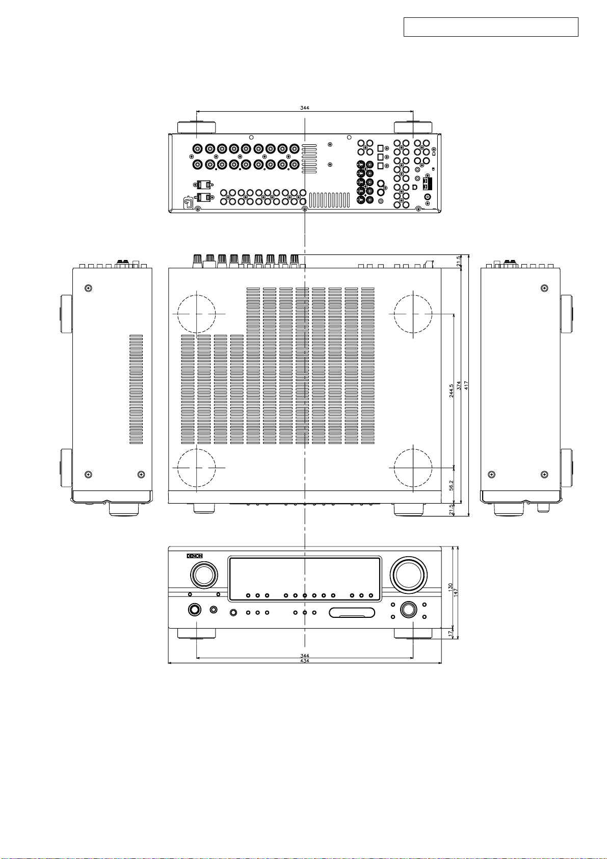
DIMENSION
AVR-1907 / AVR-787 / AVC-1630
3
AVR-1907 / AVR-787 / AVC-1630
CAUTION IN SERVICING
Initializing AV SURROUND RECEIVER
AV SURROUND RECEIVER initialization should be performed
when the µcom, peripheral parts of µcom, and Digital P.W.B. are
replaced.
1. Switch off the unit.
2. Hold the following SPEAKERS-A button and SPEAKERS-B
button, and switch on the unit.
3. Check that the entire display is flashing with an interval of
about 1 second, and release your fingers from the 2 buttons
and the microprocessor will be initialized.
Note:・If step 3 does not work, start over from step 1.
・ All user settings will be lost and this factory setting will
be recovered when this initialization mode.
So make sure to memorize your setting for restoring
after the initialization.
サービス時の注意事項
AVサラウンドアンプの初期化について
マイコンやマイコン周辺部品、Digital 基板等を交換した場合
は、AV サラウンドアンプの初期化を行って下さい。
1. オン/オフボタンを OFF にします。
2. SPEAKERS-A ボタンと SPEAKERS-B ボタンを同時に押しな
がら、オン/オフボタンを押して ON にします。
3. ディスプレイ表示が約 1秒間隔で点滅するのを確認後、2
つのボタンから指を離します。
*マイコンが初期化されます。
注意 :・上記 3 の状態にならない場合は、もう一度操作 1 か
らやり直してください。
・初期化を行うとお客様が設定した内容が工場出荷状
態に戻りますので、あらかじめ設定内容を控えてお
き初期化後再設定してください。
4
AVR-1907 / AVR-787 / AVC-1630
ADJUSTMENT
Audio Section
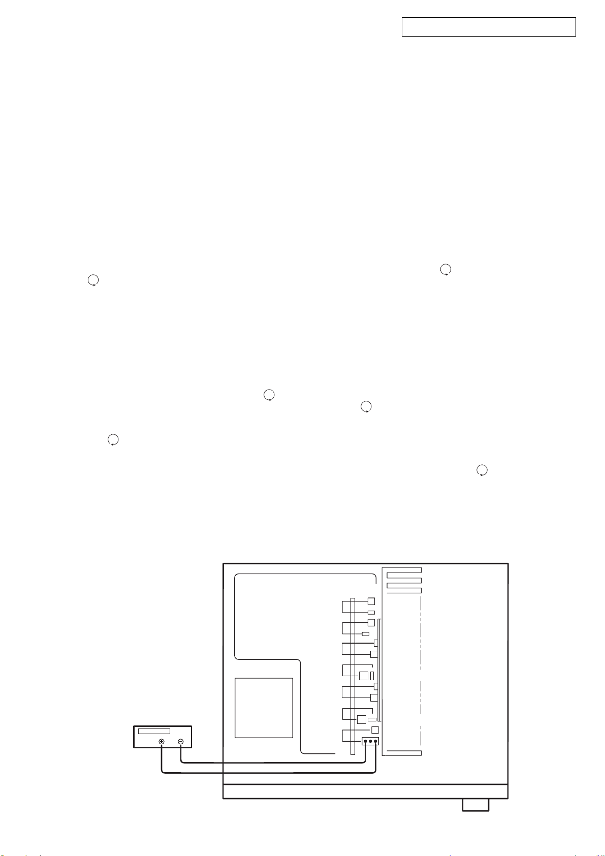
Idling Current
Required measurement equipment: DC Voltmeter
1. Preparation
(1) Avoid direct blow from an air conditioner or an electric
fan, and adjust the unit at normal room temperature 15 °C
~ 30 °C (59 °F ~ 86 °F).
(2) Presetting
• POWER (Power source switch) OFF
• SPEAKER (Speaker terminal) No load
(Do not connect speaker, dummy resistor, etc.)
2. Adjustment
(1) Remove top cover and set VR101, VR102, VR103,
VR104, VR105, on Main Amp. Unit, VR106, VR107 on
2ch-Amp. Unit at fully counterclockwise
( ) position.
(2) Connect DC Voltmeter to test points (FRONT-Lch:
TP104, FRONT-Rch: TP105, CENTER ch: TP103, SURROUND-Lch: TP101, SURROUND-Rch: TP102, SURROUND-BACK Lch: TP106, SURROUND-BACK Rch:
TP107).
(3) Connect power cord to AC Line, and turn power switch
"ON".
(4) Presetting.
MASTER VOLUME : "---" counterclockwise ( min.)
MODE : 7CH STEREO
FUNCTION : CD
(5) Within 2 minutes after the power on, turn VR101 clock-
wise ( ) to adjust the TEST POINT voltage to 1.0 mV
± 0.5 mV DC.
(6) After 10 minutes from the preset above, turn VR101 to
set the voltage to 1.0 mV ± 0.5 mV DC.
(7) Adjust the Variable Resistors of other channels in the
same way.
調整
オーディオセクション
アイドリング電流の調整
調整に必要な測定器 : DCVoltmeter
1. 準備
(1) セットをクーラ、扇風機のそばなど風通しの良い場所
を避け、通常の使用状態に置きます。セットの周囲温
度は 15〜30 ℃、湿度は常湿とします。
(2) プリセット
・電源スイッチ OFF
・スピーカ端子 無負荷
( スピーカ・ダミー抵抗器などを接続しない。)
2. 調整
(1) 上カバーをはずし、メインアンプ基板の VR101,VR102,
VR103,VR104,VR105 及び 2ch- アンプ基板の VR106,
VR107 を反時計方向 ( )に回し切った状態にセット
します。
(2) テストポイント (FRONT-Lch:TP104,FRONT-Rch:
TP105,CENTERch:TP103,SURROUND-Lch:TP101,
SURROUND-Rch:TP102,SURROUND-BACKLch:TP106,
SURROUND-BACKRch:TP107) に DCVoltmeterを接続
します。
(3) 電源コードを AC100V(95〜105Vの範囲でも可)に接
続し、電源スイッチを "ON"にします。
(4) ON後、次のようにセットします。
・MASTERVOLUME(音量調節つまみ)→反時計方向
( )に回す、最小の状態にする。
・SPEAKER(スピーカ端子)→無負荷(スピーカ、
ダミー抵抗器などを接続しない。)
MODE:7CHSTEREO
FUNCTION:CD
(5) 2分以内に VR101を時計方向 ( ) に回しテストポイ
ントの電圧を次のように調整します。
1.0mV ±0.5mVDC
(6) 予備調整から 10分後 VR101を回し、次のように電圧を
設定します。
1.0mV± 0.5mVDC
(7) 同じ方法で各チャネルの可変抵抗を調整します。
DC Voltmeter
F Lch
S Lch
S Back Rch
C ch
S Back Lch
S Rch
F Rch
5
VR104
TP104
VR101
TP101
TP107
VR107
VR103,TP103
TP106
VR106
VR102,TP102
VR105
TP105

AVR-1907 / AVR-787 / AVC-1630
VIDEO Section
(AVR-1907/787 Model)
1. SETTING
(1) Connect the oscilloscope to the Y-signal and C-signal of
S MONITOR OUT terminal and each terminate at 75
Ohms.
(2) Connect the oscilloscope to the Y-signal, P
C
B-signal, PR-signal and CR-signal of COMPONENT
MONITOR OUT terminal and each terminate at 75
Ohms.
※ Use the 75 Ohms resistance must be 1%
(3) DVD test disc : DVDT-S01
(4) COMPOSITE VIDEO OUT of DVD player is connected
to COMPOSITE : DVD.
2. BEFORE ADJUSTMENT
2.1. Setting the Oscilloscope as below.
(1) PB/CB, PR/CR, C
(a) TIME/DIV : 10μs
(b) VOLT/DIV : 100mV
(Use the probe : x10 )
(2) Y (Py)
(a) TIME/DIV : 10μs
(b) VOLT/DIV : 200mV
(Use the probe : x10 )
Power Supply
U.S.A. , Canada & Taiwan R.O.C. : 120V
Europe & Asia : 230V
China & Korea : 220V
2.2. Setup the DVD player and confirmation of the
stators
(1) Set to "INTERLACED" mode at the COMPONENT OUT.
(2) Confirm the DVD player’s out put level is equal as the
item 2.4. in following.
B-signal and
ビデオセクション
(AVC-1630Model)
1. セッティング手順
(1) セットの SMONITOROUT 端子から Y 信号と C 信号を
それぞれオシロスコープ(終端抵抗:75Ω)に接続し
ます。
(2) セットのCOMPONENTMONITOROUTの端子
B/CB,PR/CR)をそれぞれオシロスコープ
(Y,P
(終端抵抗:75Ω)に接続します。
※ 75Ω 抵抗は 1%品を使用する事。
(3) DVD テストディスク:DVDT-S01 を用意します。
(4) DVD プレーヤーの COMPOSITEVIDEOOUT を
COMPOSITE:DVD に接続します。
2. 調整のまえに
2.1. オシロスコープを下記に設定
(1) PB/CB,PR/CR,C
(a) TIME/DIV : 10μs
(b) VOLT/DIV : 100mV
(プローブ x10 使用)
(2) Y(Py)
(a) TIME/DIV : 10μs
(b) VOLT/DIV : 200mV
(プローブ x10 使用)
電源電圧
日本 : 100V
2.2. DVD プレーヤの設定と確認
(1) COMPONENTOUT の設定を " インターレース " にしま
す。
(2) DVD プレーヤーの出力が以下 2.4. 項に合っていること
を確認します。
2.3. Preparation
(1) Turn the FUNCTION knob to select "DVD" input.
(2) Push [OPEN/CLOSE] button of DVD player, then open
the Disc Tray.
Set DVD test disc (DVDT-S01) on the Disc Tray, and
then push [CLOSE] button.
(3) DVD player FL display appear "STOP", push [PLAY] but-
ton to playback DVD.
(4) Push the [DISPLAY] button of remote control of DVD
player unit and then appear the ON-Screen Display (GUI)
on the monitor TV.
(5) Push the [+10] and [2] button, select Title 12 of DVD.
(6) Push the [ENTER] button, playback Title 12.
(color bar 75%)
2.3. 準備手順
(1) FUNCTION ノブを回し、入力を "DVD" に切り替えます。
(2) DVD プレーヤーの「OPEN/CLOSE」ボタンを押しトレ
イを開き、トレイ上に DVD テストディスク(DVDTS01)をセット後、「CLOSE」ボタンを押します。
(3) DVD プレーヤーの表示管上に "STOP" が表示されてか
ら、「PLAY」ボタンを押し、ディスクを再生します。
(4) DVD プレーヤーのリモコンの「DISPLAY」ボタンを押
しグラフィカル・ユーザー・インターフェイス (GUI) 画
面を出します。
(5) 番号ボタンの「 +10 」 , 「 2 」ボタンを押し、Title12 を選択
します。
(6) 「ENTER」ボタンを押し、Title12 を再生します。
(75%カラーバー信号)
6
AVR-1907 / AVR-787 / AVC-1630
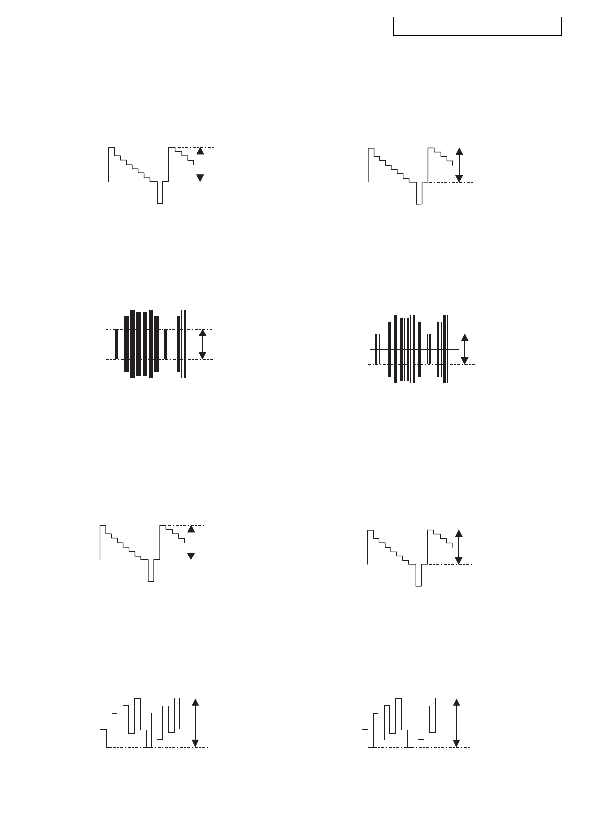
2.4. Procedure
(1) Adjust the signal of S MONITOR OUT by the wave of os-
cilloscope.
(a) Target, Y-signal
Point : COMPONENT VIDEO VR604
Adjustment Value : 714 ± 14mV
Waveform
Y
Y-signal of S MONITOR OUT
(b) Target, C-signal
Point :
Adjustment Value : 286 ± 5mV
Waveform
COMPONENT VIDEO VR605
2.4. 手順
(1) セットの SMONITOROUT の信号レベルをオシロスコー
プ上の波高値で調整します。
(a) Y 信号レベル
調整個所 : D-VIDEOVR604
調整値 : 714 ± 14mV
波形
Y
SMONITOROUT の Y 信号レベル
(b) C 信号レベル
調整個所 : D-VIDEOVR605
調整値 : 286 ± 5mV
波形
C
C-signal of S-MONITOR OUT
(2) Adjust the signal of COMPONENT OUT by the wave of
oscilloscope.
(a) Target, Y-signal
Point :
COMPONENT VIDEO VR601
Adjustment Value : 714 ± 14mV
Waveform
Y
Y-signal COMPONENT OUT
C
S-MONITOROUT の C 信号レベル
(2) COMPONENTOUTの信号レベルをオシロスコープ上の
波高値で調整します。
(a) Y 信号レベル
調整個所 : D-VIDEOVR601
調整値 : 714 ± 14mV
波形
Y
COMPONENTOUT の Y 信号レベル
(b) Target, P
Point :
B/CB-signal
COMPONENT VIDEO VR602
Adjustment Value : *525 ± 10mV
Waveform
PB/CB
PB/CB-signal COMPONENT OUT
* : 486 ± 10mV for U.S.A. & Canada model
B/CB 信号レベル
(b) P
調整個所 : D-VIDEOVR602
調整値 : 525 ± 10mV
波形
PB/CB
COMPONENTOUT の PB/CB 信号レベル
7
AVR-1907 / AVR-787 / AVC-1630
(c) Target, P
Point :
R/CR-signal
COMPONENT VIDEO VR603
Adjustment Value : *525 ± 10mV
Waveform
PR/CR
PR/CR-signal COMPONENT OUT
* : 486 ± 10mV for U.S.A. & Canada model
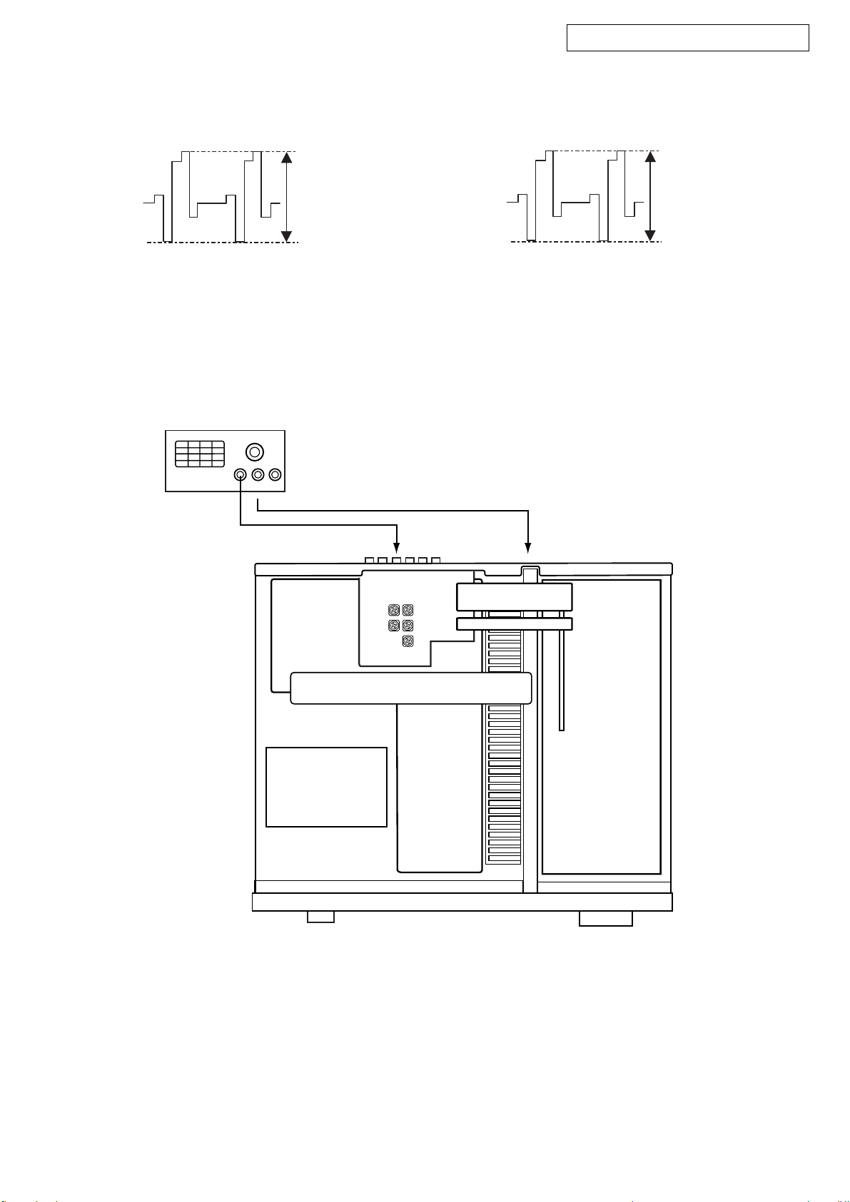
Connection method and an adjustment part.
Oscilloscope
(c) PR/CR 信号レベル
調整個所 : D-VIDEOVR603
調整値 : 525 ± 10mV
波形
PR/CR
COMPONENTOUT の PR/CR 信号レベル
接続方法と調整箇所
COMPONENT VIDEO
MONITOR OUT
(Y,P
Pb
VR602
Py
VR601
C
VR605
B/CB,PR/CR
Pr
VR603
Y
VR604
)
COMPONENT-VIDEO UNIT (AVR Model)
D-VIDEO UNIT (AVC Model)
S-VIDEO
MONITOR OUT
(Y,C)
Video Section
8
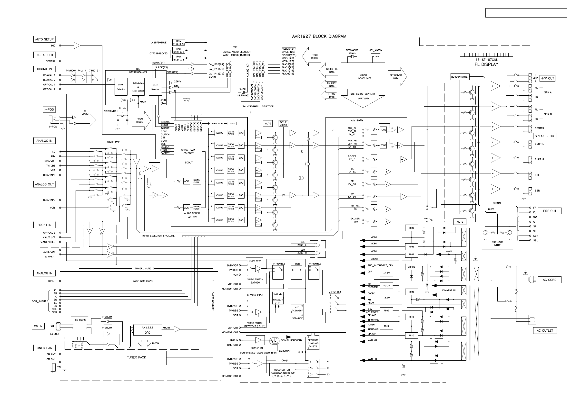
BLOCK DIAGRAM
AVR-1907 / AVR-787 / AVC-1630
9
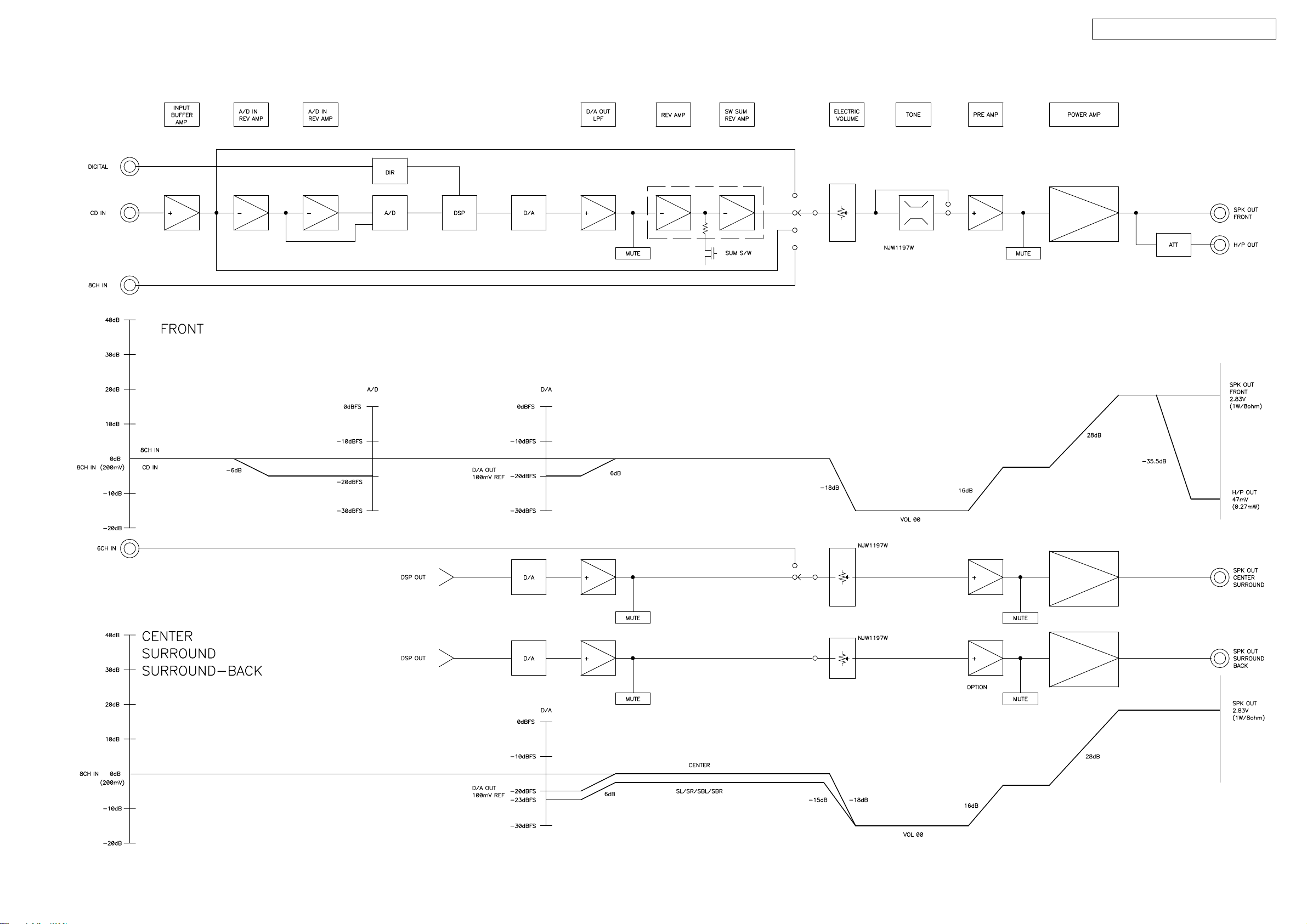
LEVEL DIAGRAMS (1/2)
AVR-1907 / AVR-787 / AVC-1630
10
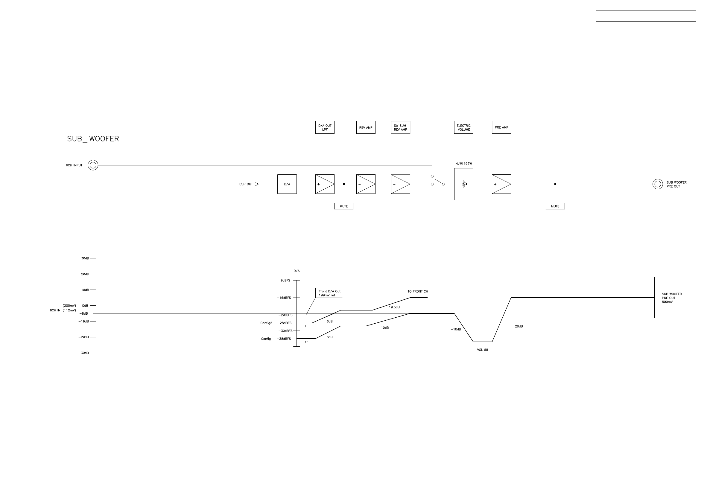
LEVEL DIAGRAMS (2/2)
AVR-1907 / AVR-787 / AVC-1630
11
SEMICONDUCTORS
E
E
E
Only major semiconductors are shown, general semiconductors etc. are omitted to list.
主な半導体を記載しています。汎用の半導体は記載を省略しています。
1. IC’s
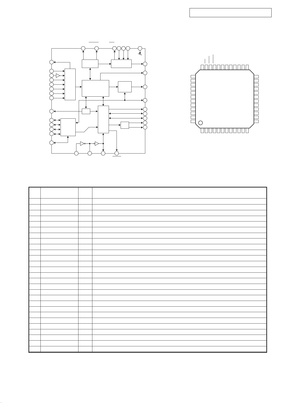
M30624FGPFP (IC201)
AVR-1907 / AVR-787 / AVC-1630
74781_CS
AVCC(+5V)
Vref(+5V)
XM_DAC_MDI
AVSSNCBAND_OPTION
100
99 98 97 96 95 94 93 92 91 90 89 88 87 86 85 84 83 82 81
Vref
P9_7
AVCC
SW_SUM 1 P9_6 P1_0 80 NJW1197_DATA
I-POD DET 2 P9_5 P1_1 79 NJW1197_CLK
BU2090_Clock 3 P9_4 P1_2 78 NJW1197_LATCH
BU2090_Data_1/74781_Data
BU2090_Data_2/74781_Clock
REMOCON 6 P9_1(TB1IN) (INT3)P1_5 75 MIC_DETECT
AD1328_SDIN 7 P9_0 (INT4)P1_6 74 BU4094_STB(XM)
BYTE 8 BYTE (INT5)P1_7 73 RDS_CLOCK
CNVSS 9 CNVSS(UP_GRADE) P2_0 72 FUNC_ENCODER_DOWN
BU4094_Data 10 P8_7 P2_1 71 FUNC_ENCODER_UP
FLD_RESET_BU4094_ENABLE
RESET 12 RESET P2_3 69 FLAG1
XOUT 13 XOUT P2_4 68 FLAG2
VSS 14 VSS P2_5 67 FLAG3
XIN 15 XIN P2_6 66 AD1328_CE
VCC1(+5V) 16 VCC1 P2_7 65 SHARC_RESET
NMI 17 P8_5 VSS 64 VSS
FLAG0 18 P8_4(INT2) P3_0 63 SHARC_SCLK
LC89057_INT 19 P8_3(INT1) VCC2 62 VCC2(+5V)
PROTECTION 20 P8_2(INT0) P3_1 61 AD1328_RESET
FLD_CLK 21 P8_1 P3_2 60 LC89057W_AD1328_SCLK
FLD_DATA 22 P8_0 P3_3 59 LC89057W_AD1328_SDOUT
FLD_CE 23 P7_7 P3_4 58 LC89057W_CE
NC 24 P7_6 P3_5 57 SHARC_SDOUT
ADV7180/7172_DATA 25 P7_5 P3_6 56 SHARC_CE
GREEN_LED 26 P7_4 P3_7 55 LC89057W_RESET
ADV7180/7172_CLK 27 P7_3 P4_0 54 EEPROM_RESET
NC 28 P7_2 P4_1 53 LC89057W_SDIN
I-POD RX 29 P4_2 52 SHARC_SDIN
I-POD TX 30 P4_3 51 LC89057_EMPHASIS
4P9_3 P1_3 77 STBY_RED_LED
5P9_2 P1_4 76 POWER_RELAY
11 P8_6 P2_2 70 H/P_DET
P7_1(RXD)
P7_0(TXD)
AVSS
P10_0
Flash = M30624FGPFP
SET_OPTION
KEY_IN3
KEY_IN2
KEY_IN1
POWER DOWN
S-VIDEO_DET
C-VIDEO_DET
COMPONENT_DET
P0_0
P0_1
P0_2
(KI0)P10_4
(KI1)P10_5
(KI2)P10_6
(AN1)P10_1
(AN2)P10_2
(AN3)P10_3
Renesas
(KI3)P10_7
S-MONITOR_DET
P0_3
BU4094_STB(MUTE)
P0_4
BU4094_STB(RELAY&MUTE)
P0_5
BU4094_STB(RELAY)
P0_6
MUTE_POWER
P0_7
P6_7(UP_GRADEP6_6(UP_GRAD
P6_5
P6_4
P6_3
P6_2
P6_1
31 32 33 34 35 36 37 38 39 40 41 42 43 44 45 46 47 48 49 50
NC
NC
XM_UART_TX
PLL_IF_COUNT
PLL DATA OUT/XM_DAC_DATA
P6_0
PLL_CE
XM_UART_RX
PLL_CLK/BU4094_CLK/XM_DAC_CLK
P5_7
TUNED
P5_6
STEREO
P5_5(UP_GRAD
NC
P5_4
VOL_ENCODER_UP
P5_3
VOL_ENCODER_DOWN
P5_2
SEL_UP
P5_1
SEL_DOWN
P5_0(UP_GRAD
NC
P4-7
NC
P4-6
RDS_DATA
P4-5
ERR_MUTE
P4-4
BSE
12
AVR-1907 / AVR-787 / AVC-1630
M30624FGPFP Terminal Function
No. Pin Name I/O/T Interrupt Pin Function
1 P9_6 O SW_SUM
2 P9_5 I I-POD DET
3 P9_4 O BU2090_Clock
4 P9_3 O BU2090_Data_1/LC74781_Data
5 P9_2 O BU2090_Data_2/LC74781_Clock
6 P9_1(TB1IN) I INT REMOCON
7 P9_0 I AD1328_SDIN
8 BYTE I BYTE
9 CNVSS(UP_GRADE) I CNVSS
10 P8_7 O BU4094_Data
11 P8_6 O FLD_RESET_BU4094_ENABLE
12 RESET I RESET
13 XOUT O XOUT
14 VSS I VSS
15 XIN I XIN
16 VCC1 I VCC1(+5V)
17 P8_5 I NMI
18 P8_4(INT2) I INT FLAG0
19 P8_3(INT1) I INT LC89057_INT
20 P8_2(INT0) I INT PROTECTION
21 P8_1 O FLD_CLK
22 P8_0 O FLD_DATA
23 P7_7 O FLD_CE
24 P7_6 O NC
25 P7_5 I/O ADV7180/7172_DATA
26 P7_4 O GREEN_LED
27 P7_3 I/O ADV7180/7172_CLK
28 P7_2 O NC
29 P7_1(RXD) I INT I-POD RX
30 P7_0(TXD) O INT I-POD TX
31 P6_7(UP_GRADE) O NC
32 P6_6(UP_GRADE) O NC
33 P6_5 I PLL_IF_COUNT
34 P6_4 O PLL_DATA OUT/XM_DAC_DATA
35 P6_3 O INT XM_UART_TX
36 P6_2 I INT XM_UART_RX
37 P6_1 O PLL_CLK/XM_DAC_CLK/BU4094_CLK
38 P6_0 O PLL_CE
39 P5_7 I TUNED
40 P5_6 I STEREO
41 P5_5(UP_GRADE) O NC
42 P5_4 I VOL_ENCODER_UP
43 P5_3 I VOL_ENCODER_DOWN
44 P5_2 I SEL_UP
45 P5_1 I SEL_DOWN
46 P5_0(UP_GRADE) O NC
47 P4-7 O NC
48 P4-6 I RDS_DATA
49 P4-5 O ERR_MUTE
50 P4-4 O BSE
51 P4_3 I LC89057_EMPHASIS
52 P4_2 I SHARC_SDIN
53 P4_1 I LC89057W_SDIN
54 P4_0 O EEPROM_RESET
55 P3_7 O LC89057W_RESET
13
AVR-1907 / AVR-787 / AVC-1630
No. Pin Name I/O/T Interrupt Pin Function
56 P3_6 O SHARC_CE
57 P3_5 O SHARC_SDOUT
58 P3_4 O LC89057W_CE
59 P3_3 O LC89057W_AD1328_SDOUT
60 P3_2 O LC89057W_AD1328_SCLK
61 P3_1 O AD1328_RESET
62 VCC2 I VCC2(+5V)
63 P3_0 O SHARC_SCLK
64 VSS I VSS
65 P2_7 O SHARC_RESET
66 P2_6 O AD1328_CE
67 P2_5 I FLAG3
68 P2_4 I FLAG2
69 P2_3 I FLAG1
70 P2_2 I HeadPhone_DET
71 P2_1 I FUNC_ENCODER_UP
72 P2_0 I FUNC_ENCODER_DOWN
73 (INT5)P1_7 I INT RDS_CLOCK
74 (INT4)P1_6 O BU4094_STB(XM)
75 (INT3)P1_5 I MIC_DETECT
76 P1_4 O POWER_RELAY
77 P1_3 O STBY_RED_LED
78 P1_2 O NJW1197_LATCH
79 P1_1 O NJW1197_CLK
80 P1_0 O NJW1197_DATA
81 P0_7 O MUTE_POWER
82 P0_6 O BU4094_STB(RLY)
83 P0_5 O BU4094_STB(RLY/MUTE)
84 P0_4 O BU4094_STB(MUTE)
85 P0_3 I S-MONITOR_DET
86 P0_2 I COMPONENT_DET
87 P0_1 I COMPOSITE_DET
88 P0_0 I S-VIDEO_DET
89 (KI3)P10_7 I INT POWER_DOWN
90 (KI2)P10_6 I INT KEY_IN1
91 (KI1)P10_5 I INT KEY_IN2
92 (KI0)P10_4 I INT KEY_IN3
93 (AN3)P10_3 I SET_OPTION
94 (AN2)P10_2 I BAND_OPTION
95 (AN1)P10_1 O NC
96 AVSS I AVSS
97 P10_0 O XM_DAC_MDI
98 Vref I Vref(+5V)
99 AVCC I AVCC(+5V)
100 P9_7 O LC74781_CS
14
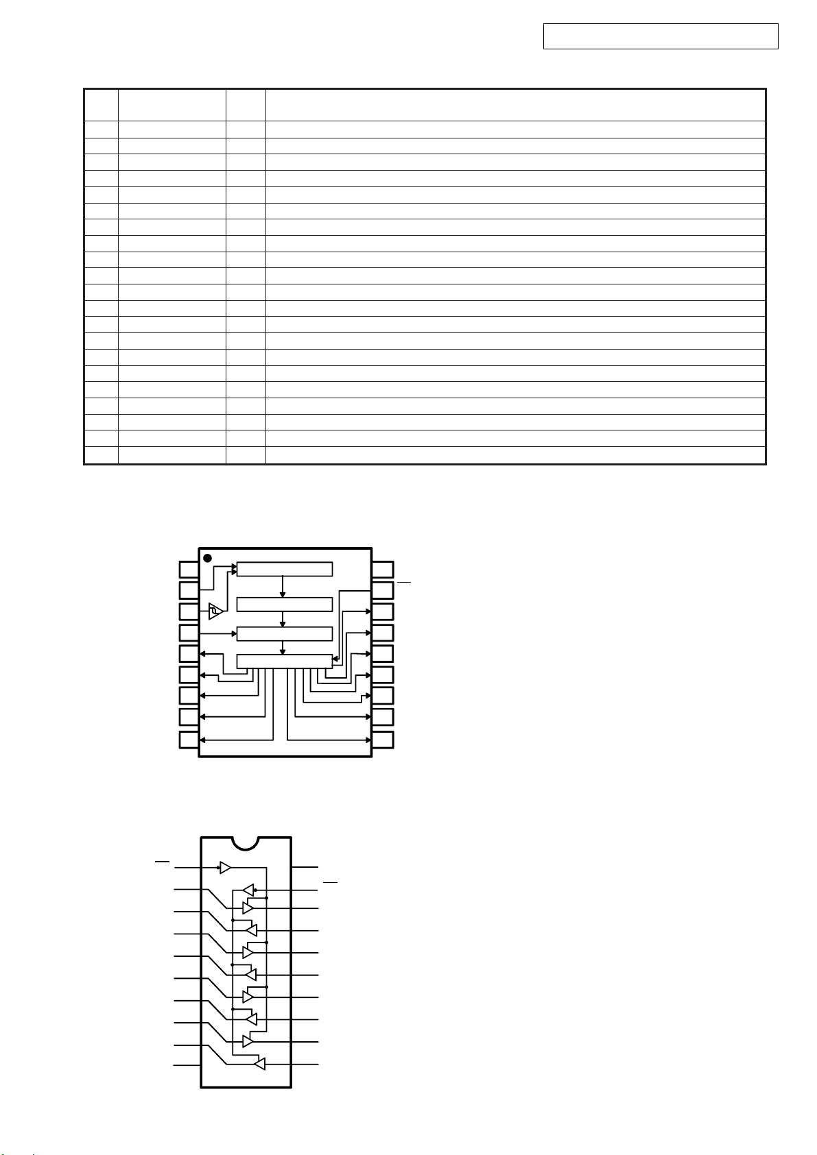
NJW1197 (IC701)
AVR-1907 / AVR-787 / AVC-1630
81
100
80
51
50
31
1
30
15
AVR-1907 / AVR-787 / AVC-1630
NJW1197 Terminal Function
No. SYMBOL FUNCTION No. SYMBOL FUNCTION
1 ROUT Rch output 51 DCR_IN Multi-channel selector Rch input
2 COUT Cch output 52 DCR_OUT Input selector Rch output
3 LSOUT LSch output 53 GND Ground
4 RSOUT RSch output 54 DCL_IN Multi-channel selector Lch input
5 LBOUT LBch output 55 DCL_OUT Input selector Lch output
6 RBOUT RBch output 56 GND Ground
7 SWOUT SWch output 57 REC_B1R Input selector Rch REC output B1
8 GND Ground 58 REC_B1L Input selector Lch REC output B1
9 FIL_BL2 Lch Bass filter terminal 2 59 REC_A4R Input selector Rch REC output A4
10 FIL_BL1 Lch Bass filter terminal 1 60 REC_A4L Input selector Lch REC output A4
11 FIL_TL Lch Treble filter terminal 61 REC_A3R Input selector Rch REC output A3
12 TCAP Switching noise rejection capacitor 62 REC_A3L Input selector Lch REC output A3
13 FIL_BR2 Rch Bass filter terminal 2 63 REC_A2R Input selector Rch REC output A2
14 FIL_BR1 Rch Bass filter terminal 1 64 REC_A2L Input selector Lch REC output A2
15 FIL_TR Rch Treble filter terminal 65 REC_A1R Input selector Rch REC output A1
16 V+ + Power supply voltage input 66 REC_A1L Input selector Lch REC output A1
17 ADR Chip address select input 67 VDDOUT Internal Digital +Power Supply Output
18 V- - Power supply voltage input 68 DATA Control data signal input
19 L1IN Input selector Lch input 1 69 CLOCK Clock signal input
20 DCCAP_SW Switching noise rejection capacitor 70 LATCH Latch signal input
21 R1IN Input selector Rch input 1 71 MUTE External Mute control
22 DCCAP_RB Switching noise rejection capacitor 72 FL+ Input selector gain control Lch no-inverted output
23 L2IN Input selector Lch input 2 73 FL- Input selector gain control Lch inverted output
24 DCCAP_LB Switching noise rejection capacitor 74 FR+ Input selector gain control Rch no-inverted output
25 R2IN Input selector Rch input 2 75 FR- Input selector gain control Rch inverted output
26 DCCAP_RS Switching noise rejection capacitor 76 GND Ground
27 L3IN Input selector Lch input 3 77 LSCIN Multi-channel LSch input C
28 DCCAP_LS Switching noise rejection capacitor 78 RSCIN Multi-channel RSch input C
29 R3IN Input selector Rch input 3 79 LBCIN Multi-channel LBch input C
30 DCCAP_C Switching noise rejection capacitor 80 RBCIN Multi-channel RBch input C
31 L4IN Input selector Lch input 4 81 GND Ground
32 DCCAP_R Switching noise rejection capacitor 82 LAIN Multi-channel Lch input A
33 R4IN Input selector Rch input 4 83 RAIN Multi-channel Rch input A
34 DCCAP_L Switching noise rejection capacitor 84 CAIN Multi-channel Cch input A
35 L5IN Input selector Lch input 5 85 LSAIN Multi-channel LSch input A
36 GND Ground 86 RSAIN Multi-channel RSch input A
37 R5IN Input selector Rch input 5 87 LBAIN Multi-channel LBch input A
38 GND Ground 88 RBAIN Multi-channel RBch input A
39 L6IN Input selector Lch input 6 89 SWAIN Multi-channel SWch input A
40 L9IN Input selector Lch input 9 90 GND Ground
41 R6IN Input selector Rch input 6 91 LBIN Multi-channel Lch input B
42 R9IN Input selector Rch input 9 92 RBIN Multi-channel Rch input B
43 L7IN Input selector Lch input 7 93 CBIN Multi-channel Cch input B
44 L10IN Input selector Lch input 10 94 LSBIN Multi-channel LSch input B
45 R7IN Input selector Rch input 7 95 RSBIN Multi-channel RSch input B
46 R10IN Input selector Rch input 10 96 LBBIN Multi-channel LBch input B
47 L8IN Input selector Lch input 8 97 RBBIN Multi-channel RBch input B
48 L11IN Input selector Lch input 11 98 SWBIN Multi-channel SWch input B
49 R8IN Input selector Rch input 8 99 GND Ground
50 R11IN Input selector Rch input 11 100 LOUT Lch output
16
ADSP21266SKSTZ-1B (IC804)
AVR-1907 / AVR-787 / AVC-1630
144
1
36
ADSP21266SKSTZ-1B Terminal Function
PIN 1 INDICATOR
37
109
108
TOP VIEW
73
72
17
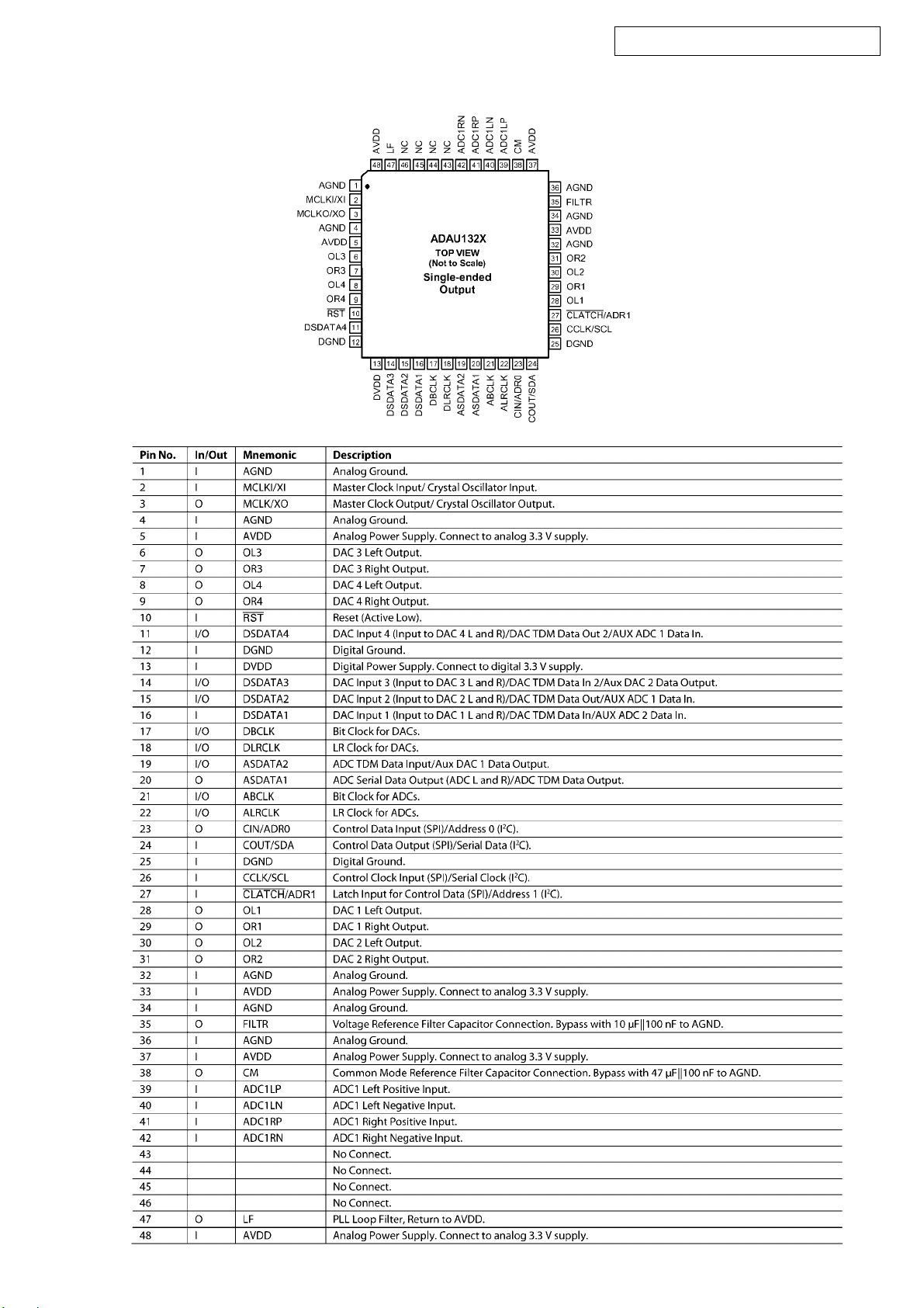
LC89057W (IC807)
AVR-1907 / AVR-787 / AVC-1630
RXOUT
RX0
RX1
RX2
RX3
RX4
RX5/VI
RX6/UI
LPF
TMCK/PIO0
TBCK/PIO1
TLRCK/PIO2
TDATA/PIO3
TXO/PIOEN
1
2
3
4
5
8
9
10
13
44
45
46
47
48
EMPHA/UO33AUDIO/VO35INT40CL39CE38DI
32
Clock
Selector
27
Microcontroller
Input
Selector
Modulation
or
Parallel Port
29
XIN
C bit, U bit
Demodulation
&
Lock Detect
PLL
28
XOUT
XMCK34CKST
I/F
Data
Selector
I/N
XMODE
41
37
36
21
24
16
17
20
22
23
DO
RERR
RDATA
SDIN
RMCK
RBCK
RLRCK
SBCK
SLRCK
36 RERR1RXOUT
35 INT2RX0
34 CKST3RX1
TOP VIEW
33 AUDIO/VO4RX2
32 EMPHA/UO5RX3
31 DGND6DGND
30 DVDD7DVDD
29 XIN8RX4
28 XOUT9RX5/VI
27 XMCK10RX6/UI
26 DVDD11DVDD
25 DGND12DGND
24 SDIN37DO
23 SLRCK38DI
22 SBCK39CE
21 RDATA40CL
20 RLRCK41XMODE
19 DVDD42DGND
18 DGND43DVDD
17 RBCK44TMCK/PIO0
16 RMCK45TBCK/PIO1
15 AGND46TLRCK/PIO2
14 AVDD47TDATA/PIO3
13 LPF48TXO/PIOEN
LC89057W Terminal Function
Pin
No.
1 RXOUT O Input bi-phase select data output ter minal
2 RX0 I TTL compatible digital data input terminal
3 RX1 I Coaxial compatible amp built-in digital data input terminal
4 RX2 I TTL compatible digital data input terminal
5 RX3 I TTL compatible digital data input terminal
6 DGND — Digital GND
7 DVDD — Digital power
8 RX4 I TTL compatible digital data input terminal
9 RX5/VI I TTL compatible digital data/Validity flag input terminal for modulation
10 RX6/UI I TTL compatible digital data/User data input terminal for modulation
11 DVDD — Digital power for PLL
12 DGND — Digital GND for PLL
13 LPF O PLL loop filter connecting terminal
14 AVDD — Analog power for PLL
15 AGND — Analog GND for PLL
16 RMCK O RMCK clock output ter minal (256fs, 512fs, XIN, VCO)
17 RBCK O/I RBCK clock in/output terminal (64fs)
18 DGND — Digital GND
19 DVDD — Digital power
20 RLRCK O/I RLRCK clock in/output terminal (fs)
21 RDATA O Serial audio data output terminal
22 SBCK O SBCK clock output terminal (32fs, 64fs, 128fs)
23 SLRCK O SLRCK clock output terminal (fs/2, fs, 2fs)
24 SDIN I Serial audio data input terminal
25 DGND — Digital GND
26 DVDD — Digital power
27 XMCK O Osc. amp output terminal
Pin Name
I/O
Function
18
AVR-1907 / AVR-787 / AVC-1630
Pin
No.
28 XOUT O X’tal osc. connecting output terminal
29 XIN I X’tal osc. connection, external clock input terminal (24.576MHz or 12.288MHz)
30 DVDD — Digital power
31 DGND — Digital GND
32 EMPHA/UO I/O Emphasis information/U-data output/Chip address setting ter minal
33 AUDIO/VO I/O Non-PCM detect/V-flag output/ Chip address setting terminal
34 CKST I/O Clock switch transition period output/Demodulation master or slave function switching ter minal
35 INT I/O Interrupt output for
36 RERR O PLL lock error, data error flag output
37 DO O com I/F, read out data output terminal (3-state)
38 DI I com I/F, write data input terminal
39 CE I com I/F, chip enable input terminal
40 CL I com I/F, clock input terminal
41 XMODE I System reset input terminal
42 DGND — Digital GND
43 DVDD — Digital power
44 TMCK/PIO0 I/O 256fs system clock input for modulation/General I/O in/output terminal
45 TBCK/PIO1 I/O 64fs bit clock input for modulation/General I/O in/output terminal
46 TLRCK/PIO2 I/O fs clock input for modulation/General I/O in/output terminal
47 TDATA/PIO3 I/O Serial audio data input for modulation/General I/O in/output terminal
48 TXO/PIOEN O/I Modulation data output/ General I/O enable input terminal
* For latch-up countermeasure, perform each power supply ON/OFF in the same timing.
Pin Name I/O
μ
com (Interrupt factor selectable)/Modulation or general I/O switching terminal
μ
μ
μ
μ
Function
BU2090F (IC1005,1008)
1
VSS
DATA
CLOCK
LCK
Q0
Q1
Q2
2
3
4
5
6
7
CONTROL CIRCUIT
12-bit SHIFT REGISTER
12-bitSTRAGE REGISTER
OUTPUT BUFFER
8
9
Q4
MM74LCX244 (IC809-811)
1
OE
2
I0
3
O4
4
I1
5
O5
6
I2
7
O6
8
I3
912
O7 O3
10 11
GND
(OPE
20
19
18
17
16
15
14
13
NDRA
N)
I
VCC
OE2
O0
I4
O1
I5
O2
I6
I7
14
18
17
16
15
13
12
11Q3
10
VDD
OE
Q11
Q10
Q9
Q8
Q7
Q6
Q5
19
ADAU1328BSTZ (IC808)
ADAU1328BSTZ Terminal Function
AVR-1907 / AVR-787 / AVC-1630
20
BA7626 (IC1004,1016,1019)
AVR-1907 / AVR-787 / AVC-1630
74LVX157MTC (IC816) BA4510F (IC815A,816A) BU4094BCF (IC208X,551-553)
SE
LECT
1A
1B
1Y
2A
2B
2Y
GND
1
STROBE
1
2
SEL
3
4
5
5
6
7
8
16
15
14
13
12
11
10
Vcc
ST
4A
4B
4Y
OUT1
Ð IN1
+ IN1
1
2
1ch
+
Ð
3
2ch
+
Ð
VCC
8
OUT2
7
Ð IN2
6
3A
3B
9
3Y
EE
V
4
+ IN2
5
SERIAL
IN
CLOCK
V
2
3
4
1
Q
5
Q2
6
Q3
7
Q4
8
SS
16
15
14
13
12
11
10
9
V
DD
OUTPUT
ENABLE
Q5
Q6
Q7
Q8
Q'S
QS
MM74HCT244 (IC812) FAN1117-1.2 (IC824)
RC1117-33 (IC823)
201
V
1G
1A
2Y
1A
2Y
1A
2Y
1A
2Y
GND
0
0
1
1
2
2
3
3
CC
192
2G
0
183
1Y
0
174
2A
1
165
1Y
1
156
2A
2
147
1Y
2
138
2A
3
129
1Y
3
1110
2A
V
OUT
2
3
2
1
IN
OUT
ADJ/GND
21
LH28F800BJE (IC805)
SN74LV573APWR (IC818,819)
AVR-1907 / AVR-787 / AVC-1630
1
OE
2
D0
3
D1
4
D2
D3
5
6
D4
7
D5
8
D6
9
D7
GND
10
SN74LVC139APWR (IC820)
1
16
15
14
13
12
11
10
V
CC
2G
2A
2B
2Y0
2Y1
2Y2
9
2Y3
1G
1A
1B
1Y0
1Y1
1Y2
1Y3
GND
2
3
4
5
6
7
8
Vcc
20
19
18
17
16
15
14
13
12
11
Q0
Q1
Q2
Q3
Q4
Q5
Q6
Q7
LE
OE
234
11
E
1
D0
D
Q
L
Q0 Q1
D1 D2
D
Q
L
1819
D3 D4 D5 D6
D
L
Q
L
17
Q2
FUNCTION TABLE
(each decoder/demultiplexer)
INPUTS
G
G
SELECT
B A Y3 Y2 Y1 Y0
OUTPUTS
OUTPUTS
L L L H H H L
L L HHHLH
L H LHLHH
L H HLHHH
H X X H H H H
567
D
D
Q
L
Q
L
16
Q4 Q5 Q6 Q7
Q3
89
D
Q
L
D7
D
D
Q
L
Q
L
12131415
SN74LV14APWR (IC829) MM74HCT00MTCX (IC814,815)
1A
1Y
2A
2Y
3A
3Y
GND
1
2
3
4
5
6
7
Vcc
14
13
6A
6Y
12
5A
11
5Y
10
4A
9
4Y
8
1A
1B
1Y
2A
2B
2Y
GND
2
3
4
5
6
7
Vcc
14
4B
13
4A
12
4Y
11
3B
10
9
3A
3Y
8
1
22
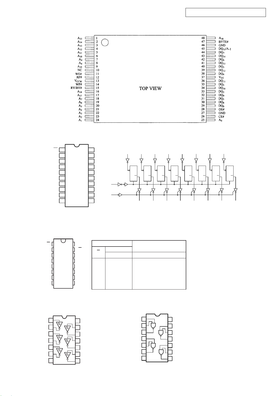
AS7C34096A-10TCN (IC806,817)
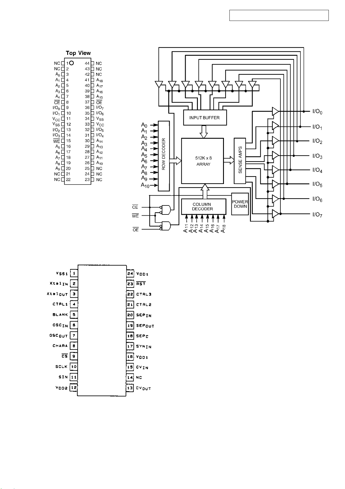
AVR-1907 / AVR-787 / AVC-1630
LC74781 (IC1012)
23
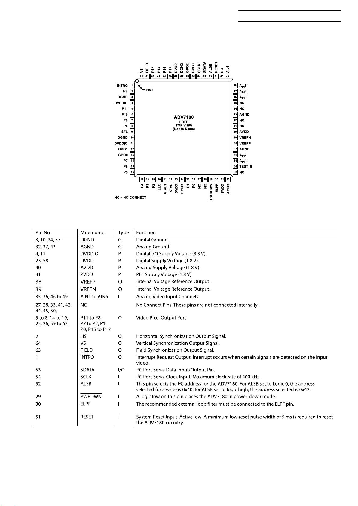
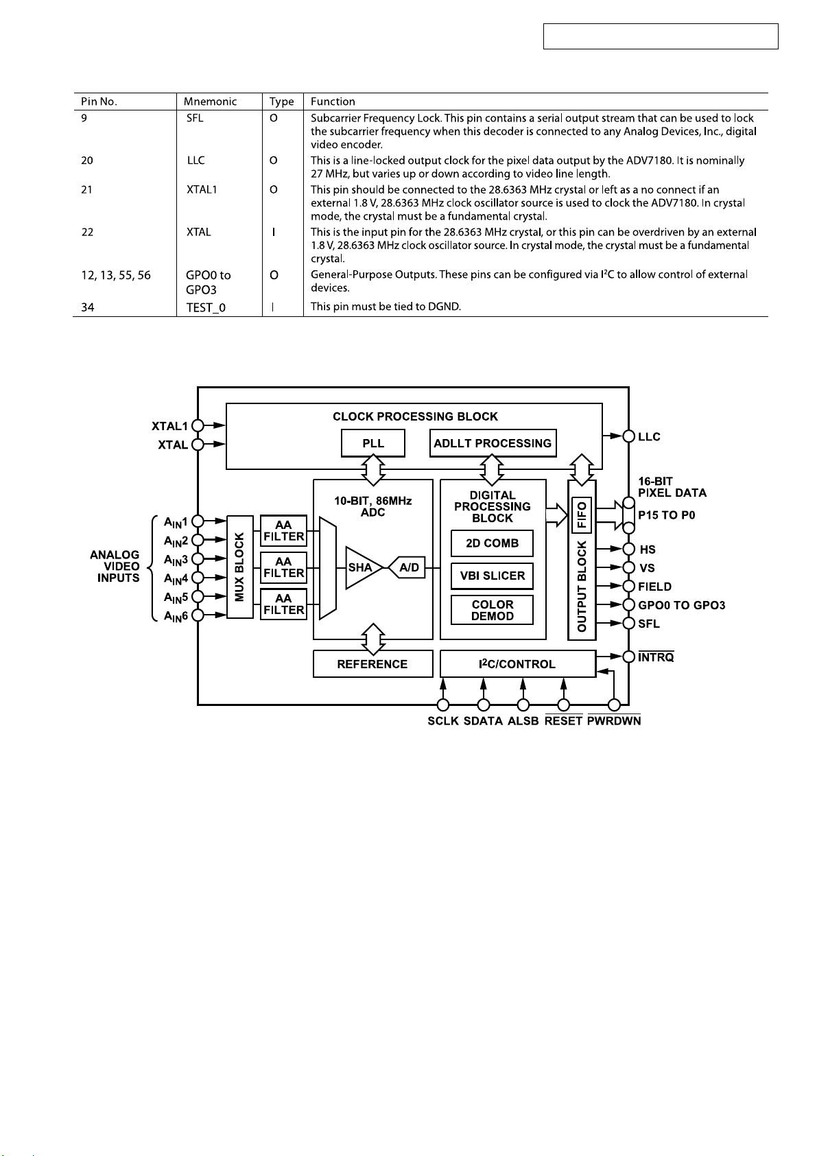
ADV7180BSTZ (IC601)
AVR-1907 / AVR-787 / AVC-1630
24
AVR-1907 / AVR-787 / AVC-1630
25
ADV7172KSTZ (IC602)
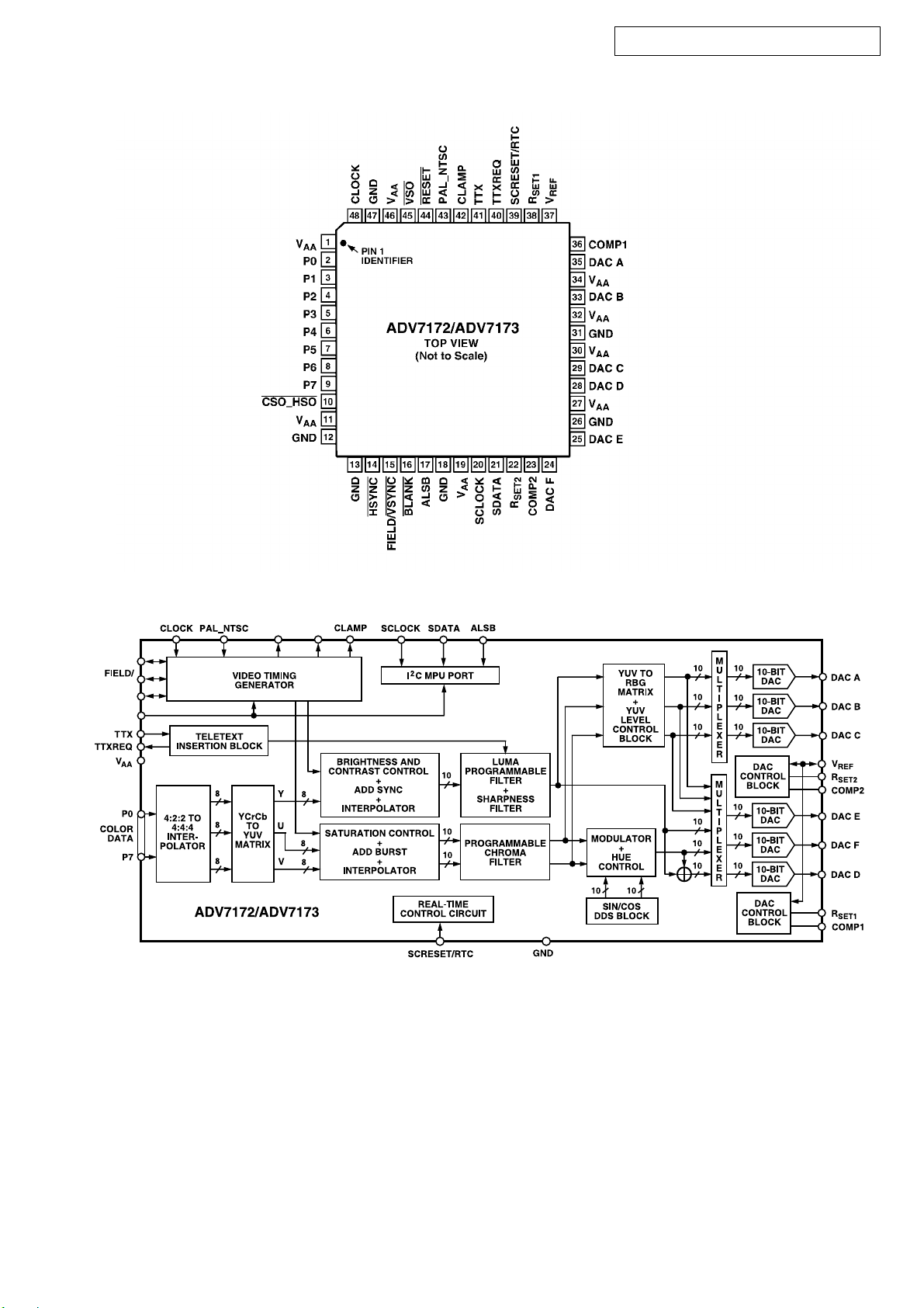
AVR-1907 / AVR-787 / AVC-1630
26
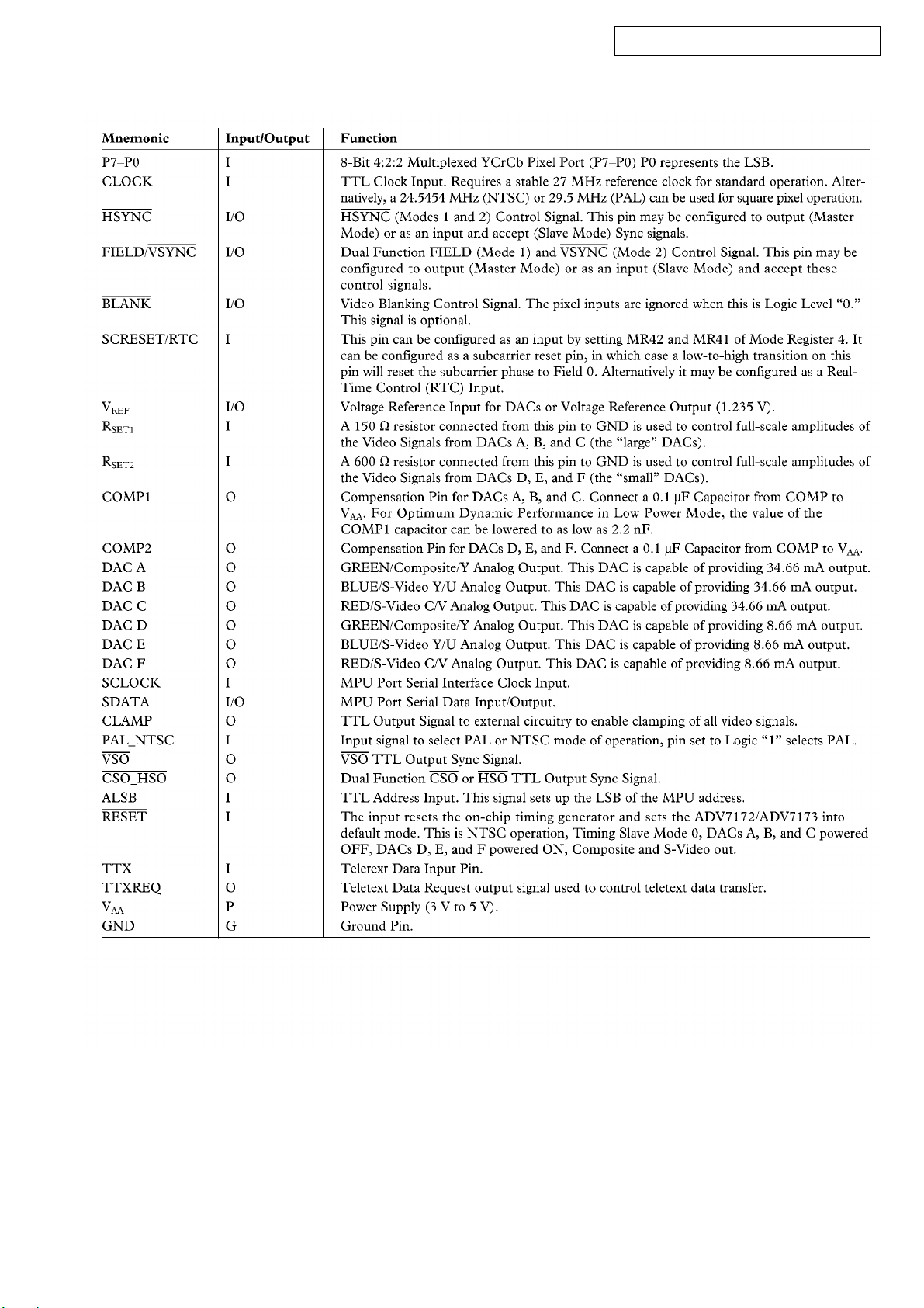
PIN FUNCTION DESCRIPTION
AVR-1907 / AVR-787 / AVC-1630
27
2. FL DISPLAY
16-ST-87GINK (FL301)
AVR-1907 / AVR-787 / AVC-1630
28
AVR-1907 / AVR-787 / AVC-1630
29
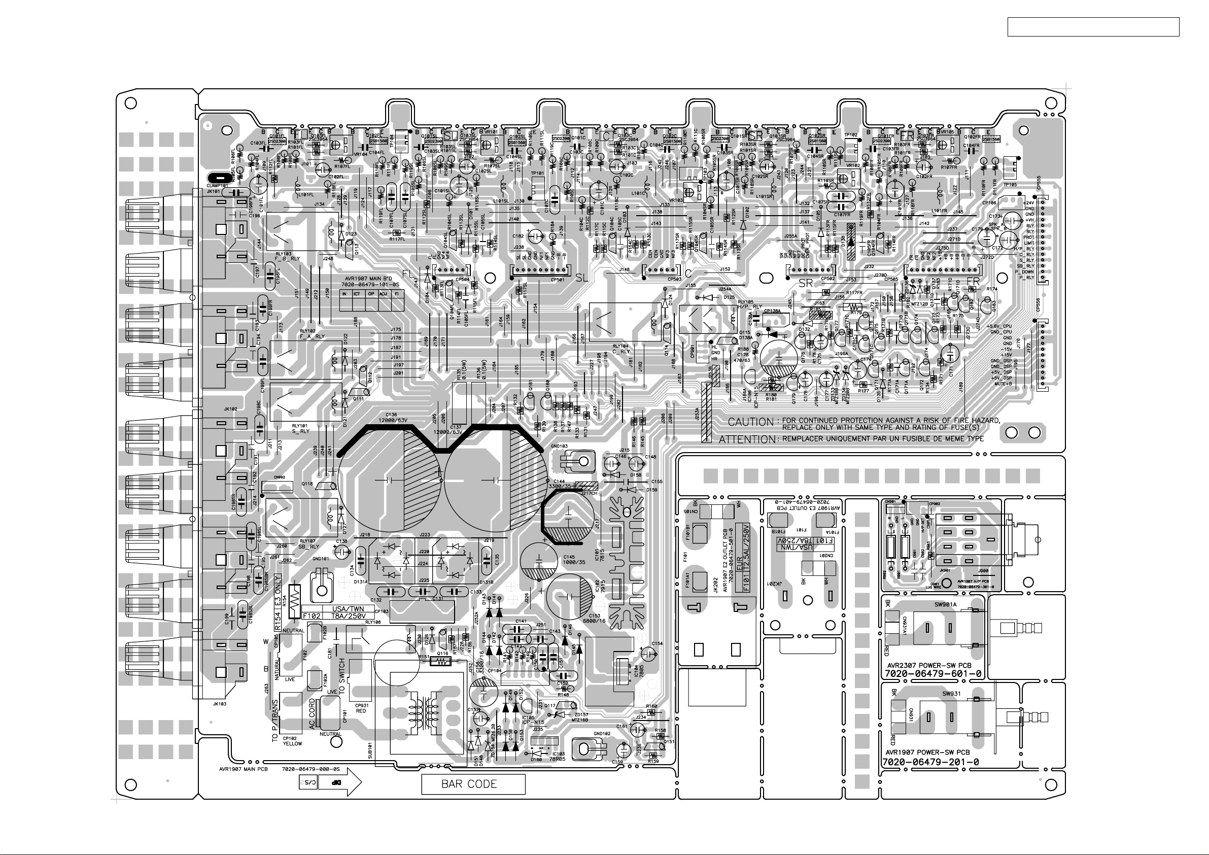
PRINTED WIRING BOARDS
MAIN P.W.B. UNIT (1/2)
AVR-1907 / AVR-787 / AVC-1630
DENON
DENON
DENON
DENON
DENON
30
DENON
COMPONENT SIDE
 Loading...