

Page 1
VP520S
VP520S
PAL/NTSC to CIF/QCIF Converter
Advance Information
Supersedes version in June 1995 Digital Video & DSP IC Handbook, HB3923-2 DS3504 - 3.2 October 1996
FEATURES
■ Lower Power, pin compatible replacement for VP520
■ Converts CCIR601 luminance and chrominance to CIF
or QCIF resolution, and vice versa, using a 27MHz
system clock.
■ Luminance and chrominance channels have their own
sets of horizontal and vertical filters with on chip line
stores
■ Each filter set may be configured to either decimate or
interpolate.
■ NTSC line insertion or removal mode
■ Produces / expects CIF/QCIF data in macroblock for-
mat.
■ 120 Pin QFP Package
ASSOCIATED PRODUCTS
■ VP510 Colour Space Converter
■ VP2611 H261 Encoder
■ VP2615 H261 Decoder
■ VP2612 Video Multiplexer
■ VP2614 Video Demultiplexer
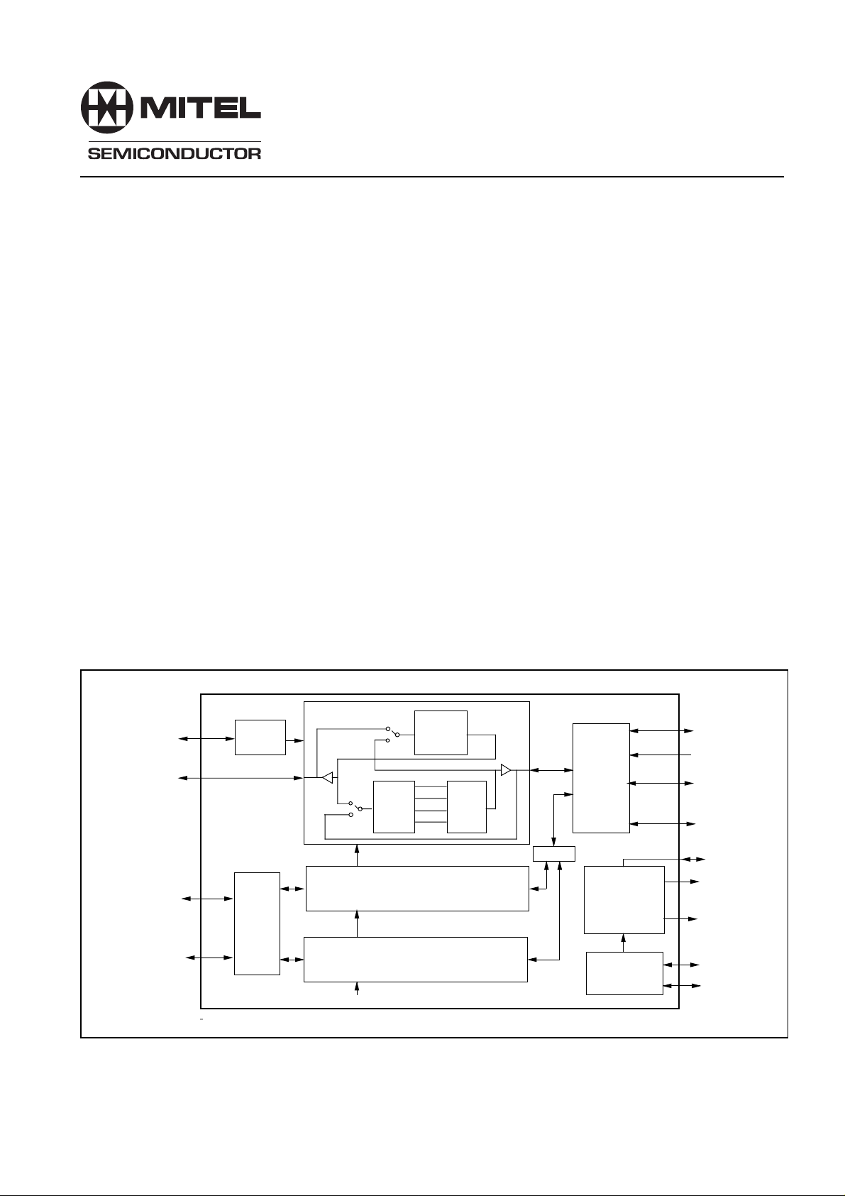
DESCRIPTION
The VP520S is designed to convert 16 bit multiplexed
luminance and chrominance data between CCIR601 and CIF/
QCIF resolutions. Vertical and horizontal FIR filters are provided, with the vertical filters supported by on chip line stores.
The coefficients used by the filters are user definable, and are
down loaded from an independent host data bus. An internal
address generator supports an external DRAM frame store,
and also provides line to macroblock conversion.
When producing CIF or QCIF video the horizontal filters
precede the vertical filters, and are provided with between 8
and 16 taps. The vertical filters are provided with four CIF line
delays which allow a 5 tap filter to be implemented. When
producing QCIF the available RAM is used to provide six line
delays, which thus allows 7 tap filters to be used.
When the device is producing CCIR601 video, the incoming data must be in macroblock format, and the vertical filters
precede the horizontal filters The inputs are firstly written to a
external CIF sized frame store, and are read out in line format.
The VP520S will support two complete frame stores, and
allows the CIF/QCIF data to be read out twice in order to
produce two interlaced fields of video.
The VP520S supports the conversion between CIF/QCIF
and NTSC video. An extra line is produced for every five lines
when producing CIF data, and one line in six is removed when
producing NTSC video. Poly phase filters are used to provide
the correct decimation and interpolation ratios.
HOST
BUS
8 BIT
LUMINANCE
8 BIT
CHROMINANCE
CREF
COEFF
STORE
MUXING
MUXING
FILTER BLOCK
Horizontal
FOUR
LINE
DELAYS
FILTER BLOCK
FILTER BLOCK
Filters
Fig 1 : Simplified Block Diagram
Vertical
Filters
MUX
VP520S
INPUT/
OUTPUT
FIFO
RAM ADDRESS
GENERATOR
SUPPORTING
LINE TO BLOCK
CONVERSION
SYNC
GENERATOR
MACROBLOCK
STROBE
REQ BLKS
8 BIT
MACROBLOCK
BUS
16 BIT
FRAME STORE
BUS
FRAME START
/ READY
ADDRESS
CONTROL
HREF
VREF
1
Page 2
VP520S
PIN DESCRIPTION
NAME TYPE FUNCTION
Y7:0 I/O Luminance input or output bus
C7:0 I/O Chrominance input or output bus
M7:0 I/O Macroblock input or output bus
D15:0 I/O 16 bit data bus for DRAM frame store
A7:0 O Multiplexed address bus to the DRAM
A8 O Most sig address bit or second CAS
RAS O Row strobe for the DRAM's
CAS O Column strobe for the DRAM's
R/W O Read/ write signal to the DRAM's
HREF I/O Horiz. reference in or horiz. sync out
VREF I/O Vertical reference in or vertical sync out
CREF I/O CREF in or CREF out
FREF I/O Field Indicator in or out
HBLNK O Horizontal Blanking output
CSYNC O Composite sync output in free run mode
CLMP O Defines a black level clamping period
for A/D converters
VRST Frame start identifier. If FRST is low
then a low going edge will reset the
internal sync generator.
FRST Field identifier
REQYUV I Request macroblocks from encoder
MCLK I/O Macroblock I/O strobe
FSIG I/O Frame start/ ready signal
SCLK I System Clock. 27MHz in PAL/NTSC
systems
HD7:0 I/O Host data bus
HA3:0 I Host controller address bits
RD I An active low host read strobe
WR I An active low host write strobe
CEN I An active low enable for the strobes
RST I Power on reset
TDI I JTAG I/P data
TDO O JTAG O/P data
TMS I Test mode select
TCK I JTAG clock
TRST I JTAG reset
TOE I When high all O/P's are high
impedance
NOTE:
"Barred" active low signals do not appear with a bar in the main
body of the text.
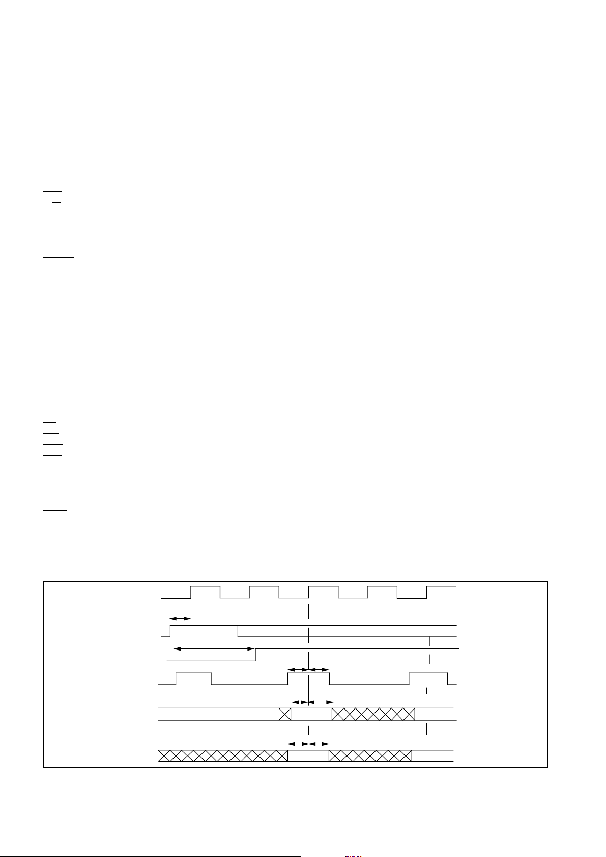
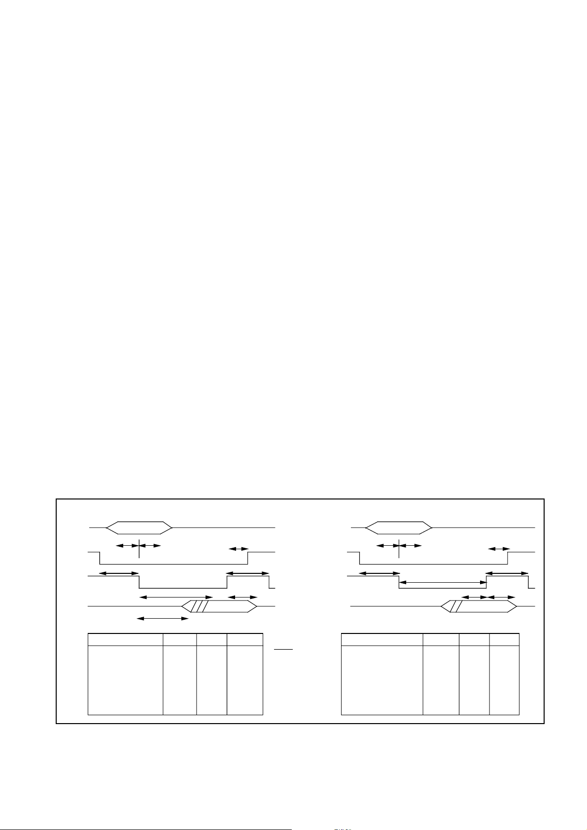
VIDEO COMPRESS MODE ( DECIMATE )
This mode is used when CCIR601 video is to be converted
to CIF or QCIF spatial resolution prior to compression. Incoming luminance and chrominance data does not need any prior
buffering, but must meet the timing requirements given in
Figure 2. A bit in Control register 1 allows the Cb component
to precede the Cr component if necessary. This data is passed
through vertical and horizontal decimating filters before it is
stored in an external frame store. When a complete field has
been decimated it is read out in macroblock format and
transferred to the next system component.
In this mode HREF, VREF, and FREF are normally inputs
which are used to reference active video with respect to video
synchronization pulses. The active going edges are used
internally, and these must meet the set up time with respect to
the system clock as given in Figure 2. Stable inputs are
needed with no jitter due to asynchronous pixel clocks, but
when this is not possible an external FIFO can be used plus
two extra signals as described later. The reference inputs
need only stay active for one system clock period. Note that
the active going edges for HREF and VREF can individually
be defined to be high going or low going, through two bits in
Control Register 0. Also note that CREF is always an input and
is used as a qualifier for SCLK. The actual edges of CREF are
not used.
The internal sync generator can still be used in this mode,
if there is a need to supply sync to the video source. The HREF
and VREF pins are then used to output HSYNC and VSYNC.
Composite sync is supplied on the CSYNC pin.
In addition the CLMP pin provides a pulse [13 SCLK's
wide] which can be used to DC restore the black level in an A/
D converter. It is active high during the back porch.
The horizontal blanking output (HBLANK) defines when
the device expects the first pixel in a line to be supplied, and
is derived from the user supplied HREF input. The delay
between HREF and HBLANK is user definable in multiples of
CREF periods. If the defined value is zero then the HREF input
must be horizontal blanking with the minimum set time specified. The HBLANK output is then not defined.
All data changes are referenced to the system clock. The
edge actually used is indicated by the CREF input signal,
which has a period of double the clock period. The VP520S will
strobe in data on the rising edge of the system clock which
occurs whilst CREF is high.
INPUT
CLOCK
10ns min
HREF
INPUT
HBLNK
O/P
CREF
INPUT
LUM
INPUT
CHROM
INPUT
PROGRAMMED DELAY
2ns
10ns
min
min
10ns
min
2ns
10ns
min
min
First Cr Comp.
2ns
min
Second I/PFirst I/P
First Cb Comp.
Fig 2 : Luminance and chrominance inputs in the decimate mode.
2
Page 3
VP520S
The first video line to be filtered and stored will be derived
from the vertical reference input ( VREF). The user can choose
the number of transitions of the HREF input which must occur,
after VREF has gone active, before starting the filter operation. Data is then not written to the DRAM until after the
pipeline delay through the filters.
The VP520S only expects to use one field of CCIR601
video, which can be selected by the FREF input or internal
logic. A bit in Control Register 1 ( Internal / External Field
Detect ) determines which option is to be used. An additional
Field Select Bit determines whether the field selected should
correspond to FREF being high or low. When the Field Select
Bit and the input are at the same logical level then that field is
used. Note that FREF transitions must be coincident with
active going VREF transitions.
Internal logic is provided which determines the field ( Field
1 ) in which VREF goes active in less than half a line period
after the HREF input last went active.The half line period is
determined by VREF going active between 1 and 432 CREF
qualified SCLK edges after HREF went active (1-429 in NTSC
mode). Note that coincident VREF and HREF edges will
indicate this field on the first CREF qualified SCLK edge.
This logic is used, rather than the FREF input, when the
Internal / External Field Detect Bit is low. Field 1 is selected
when the Field Select in Control register 1 is low, and Field 2
is used when the bit is high.
In the Split Screen mode this logic is overridden, and both
fields are actually used. External logic is assumed to switch
between two sources of video, one for each field. The internal
DRAM address generator is modified such that half area
pictures from the centre of each source are actually stored as
CIF/QCIF data. The first line used in each field will be 72 line
delays in addition to the number which has been defined by the
user. The split screen option is not supported in the QCIF
mode of operation, and a reset is needed after a mode change
in CIF.
The VP520S will insert zero's into the line delays during
vertical blanking. This ensures that all the filter accumulators
are cleared and the edges of the picture are correctly processed. The horizontal filters always give the required results
since four decimated values are ignored at either side of the
picture.
Incoming luminance data could have a black level of 16,
which will be shifted if the filter coefficients are not chosen to
exactly give a gain of unity. A Control Bit is thus provided,
which when set causes 16 to be subtracted from incoming
luminance. A black level of zero will then stay as zero throughout the filter operation. At the output of the filters 16 is always
added to the results, regardless of the state of the Control Bit.
Saturation logic ensures that these addition / subtraction
operations do not produce negative results or values greater
than 254.
A Control Bit is also provided which selects between colour
difference inputs and true Cr Cb chrominance values. Cr Cb
values are 8 bit positive only numbers, with black levels of 128.
These must be converted to two's complement signed numbers by subtracting 128, thus giving a black level of zero
through the filters. The outputs of the filters are always
converted to positive only Cr Cb values by adding 128 to the
results, regardless of the state of the Control Bit.
COPING WITH SYNC JITTER
When input syncs to the VP520S have jitter, due to the use
of a composite video decoder which does not produce a line
locked clock, it is necessary to use an external FIFO line
buffer. For this reason the VP520S supports a system in which
external line buffer writes are controlled by the video source
and line reads are controlled by the VP520S. The VP520S in
the decode loop is assumed to be supplying sync to the
VP520S in the encode loop, but the sync generator must be
reset at the start of a frame to be in step with the video source.
Two pins have been supplied to support this situation, namely:
VRST - pin 34, and FRST - pin 36. The falling edge of VRST
(frame start identifier) when FRST (field identifier) is low
identifies the start of the frame. These two inputs can typically
be supplied by the Brooktree Bt812 Composite Video Decoder. Note that Host Address 3 must be programmed with
the value 02 Hex to enable the reset operation.
CIF/QCIF MACROBLOCK OUTPUTS
When producing decimated CIF/QCIF data in macroblock
format, the device raises a flag when a frame of data is ready
for reading from the frame store ( FSIG ). The FSIG pin is
automatically configured as an output in the decimate mode,
but will only stay active (high) for the time given in Figure 3. If
a Request Macroblock response (REQYUV) is not obtained
during this period, then FSIG will be taken low and the frame
of data presently available will be ignored. It will go high again
when a new frame of data is available.
SYSCLK
FSIG
O/P
REQYUV
I/P
MCLK
O/P
DATA
O/P
20ns
max
33ns min
Stays high for 11440 (NTSC) or 13284 (PAL) SCLKs if REQYUV not received
20ns max
10ns
2ns
min
min
60 SYSCLK Max , 10SYSCLK Min
20ns max
Fig 3 : Macroblock Output Timing
20ns max
First O/P Valid O/P Valid
20ns max
3
Page 4
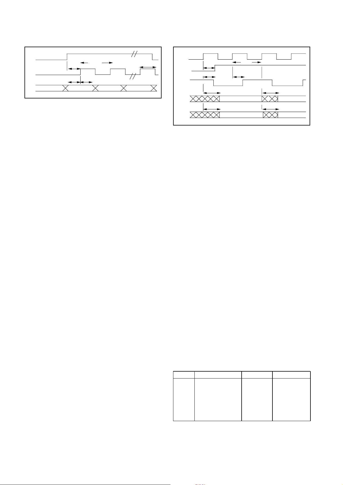
VP520S
-
-
-
-
-
-
-
FSIG
I/P
MCLK
DATA
I/P
40ns min
I/P
10ns min 2ns min
4SCLK min
40ns min
Second I/PFirst I/P
Fig 4 : Macroblock Input Timing
When it receives a REQYUV response from the next
system component, it starts to output a macroblock by using
an output strobe derived by dividing down the clock input.
Detailed timing is given in Figure 3. This strobe only occurs
when data is available at the output pins and at a rate of
SYSCLK/4. The 'Request Macroblock' flag must go inactive
and then active again before a further macroblock is made
available.
The Frame Ready flag is only available on the output pin
if the Frame Enable Bit is set in Control Register 1. Through
this control bit a host controller is able to determine whether a
new frame is to be compressed and transmitted. In an alternative arrangement the control bit can be permanently set, and
the Frame Ready Flag is then used as an interrupt to the host
controller. It then generates a signal which is used as the
Frame Ready signal for the next device.
The following sections describe this interface as it applies
to the VP2611 H261 Video Encoder.
TRANSFERING MACROBLOCKS TO THE VP2611
When the VP520S has stored a complete field of decimated video in the DRAM, it raises a Frame Ready Flag ( FSIG
). If the bit in Control Register 1 does not inhibit the output, this
flag becomes the FRMIN input on the VP2611. This responds
to the FRMIN input by generating a Request for Macroblock
Data ( REQYUV ). The VP2611 MUST then receive a complete macroblock ( 384 bytes ) within 1870 cycles of the
system clock. When the VP520S is producing decimated CIF/
QCIF data, writing line data to the DRAM has priority, and only
four macroblock read operations are possible in every 32
clock cycles i.e. one read takes eight cycles. These, however,
are 16 bit word operations and it thus requires 384 x 8/2 = 1536
cycles to output the data. In addition there is a maximum delay
of 60 clock periods from receiving REQYUV to producing the
first output strobe (MCLK). This is still well within the time
available.
The four 16 bit words are stored in the VP520S and
transmitted to the VP2611 as eight bytes using a strobe
( MCLK ) derived from the system clock. This is only present
when valid data is available, and it drives the PCLK input on
the VP2611.
It takes the VP2611 almost exactly all the available time at
30 Hz frame rates to process all the macroblocks. After a field
time ( half an interlaced frame ) the VP520S will start to write
new data to the DRAM, and data could be overwritten during
the last macroblocks. Since there is available space in the
DRAM, a small address offset is used between video fields to
avoid this problem.
INPUT
CLOCK
HBLANK
O/P
CREF
O/P
LUM
OUTPUT
CHROM
O/P
20ns
max
20ns max
20ns max
20ns max 20ns max
33ns min
20ns
max
First O/P Valid
First Cr Component Valid
20ns max
Second O/P Valid
First Cb
Fig 5 : Luminance and Chrominance Output Timing
INTERPOLATE MODE
In this mode the VP520S expects to receive CIF/QCIF
data in macroblock format, which it then writes to an external
frame store. This is then read back in line format and passed
through vertical and horizontal interpolating filters to produce
two fields of CCIR601 video. Detailed input timing is given in
Figure 4.
FSIG automatically becomes an input which is used to
identify the start of a frame and to reset the internal address
counter. FSIG must stay high until a complete CIF/QCIF frame
has been received ( internal logic counts macroblocks ). If
FSIG goes low early then the complete frame will be ignored,
and the previously received frame will continue to be displayed.
An input strobe, derived by dividing the system clock by
four, must also be provided in order to input data. This must
only be present when valid data is available on the input pins.
Incoming macroblocks are byte wide, and these are internally
buffered to allow four 16 bit words to be written to the DRAM
every 32 system clock cycles. This is equivalent to a byte input
rate of SCLK/4 which must not be exceeded.
The CIF frame store is double buffered such that a new
frame can be received whilst the previous one is being
displayed. In fact the use of 256K x 16 DRAM's gives sufficient
capacity for more than three complete CIF frames, and the
internal address generator will simply roll around to make full
use of the available space.
Once a complete CIF/QCIF frame has been received, it will
normally be used to generate two interlaced PAL or NTSC
fields. These fields continue to be re-generated until a complete new CIF frame has been received. The rate of receiving
frames depends on the transmission bandwidth, but the
maximum rate is 30 Hz. The changeover to the newly received
frame will occur when the VP520S has finished generating
any one of the pair of interlaced fields for display, it does not
SYMBOL PARAMETER MINIMUM MAXIMUM
t RAC Access time from RAS
t CAC Access time from CAS
t RP RAS precharge time 50ns or under
t CP CAS precharge time 12ns or under
t RAS RAS pulse width 80ns or under
t CAS CAS pulse width 50ns or under
t REF Time between
complete refreshes
105ns or under
25ns or under
4 ms or over
(8 ms with 256k x n)
N.B. All times are quoted assuming 27MHz operation. For lower clock
frequencies increase the above values proportionately.
4
Table 1. External DRAM Timing Requirements
Page 5
VP520S
necessarily have to have generated two interlaced fields from
the received frame. If the VP520S is receiving frames at the
full CIF 30 Hz frame rate but only displaying PAL frames at 25
Hz, then periodically one of the PAL frames ( comprising two
interlaced fields at 50 Hz ) will be generated from two received
CIF/QCIF frames. An incoming CIF/QCIF frame will always be
used since the interlaced field rate is always greater than 30
Hz in either PAL or NTSC.
The data is read from the frame store such that interpolated data becomes available after programmed delays referenced to the VREF and HREF signals. Six bits are available
to define the line delay, and ten are provided to define the
delay from HREF in CREF periods. The actual delays are
greater than the programmed values because of the internal
pipeline delays, which are also mode dependent.
HREF and VREF can either be user supplied inputs, or are
generated internally from a PAL/NTSC timing generator. A bit
in Control Register 0 determines this option, and when the
internal generator is specified the HREF pin becomes an
output which supplies horizontal sync and the VREF pin
supplies vertical sync. A composite sync output is also provided for system level use. In this mode the VREF and HREF
signals used internally are effectively vertical and horizontal
sync, and the programmed delays should be chosen to reflect
this condition.
The signals provided from the internal timing generator
allow the VP520S to drive the VP510 Colour Space Converter
and an RGB monitor. Detailed output timing is given in Figure
5. Note that the chrominance order can be changed. Alternatively they can be used to drive off the shelf composite video
encoders.
External chrominance data can have a zero colour difference value of either 0 or 128. This is defined using the
Chrominance Control Bit. Where 128 is the zero colour
difference value, 128 will be subtracted from incoming
chrominance data and 128 will be added to output chrominace
data. Output values will be limited to lie in the range 16 to 240.
External luminace data can have a black luminace level of
either 0 or 16. This is defined using the Luminace Control Bit.
Where 16 is the black value, 16 will be subtracted from
incoming luminace data and 16 will be added to output
luminace data. Output values will be limited to lie in the range
16 to 235.
The data stored in the CIF frame store will not contain the
black levels normally present during horizontal and vertical
flyback. This is inserted by the VP520S at the appropriate
times in order to ensure that the correct filter operation occurs
at the edges of the picture. In addition to these black levels
during flyback, a bit in Control Register 1 allows all active video
to be replaced by a fixed colour. This colour is user definable
through YUV values in three registers.
FRAME STORE INTERFACE
All read and write operations to the external DRAM frame
stores are based on the use of fast page mode with 13.5 MHz
CAS cycles. Internally a 54 MHz clock is produced from the
27MHz System clock, and this determines the minimum time
interval which can be used in the generation of pulses and
defining precharge times. Any DRAM used must meet the
timing constraints given in Table 1.
Reading and writing rates dictate the need for a 16 bit data
interface, and line data is re-organized to allow a 16 bit word
to consist of either two luminance values or two chrominance
values. This gives compatibility with the macroblock requirements since a sub block is either all chrominance or all
luminance data. Reading or writing macroblock data requires
jumps between pages, but four words can always be read or
written using fast page mode.
Read and write operations must be timeshared to meet the
requirements of the system. This time-sharing is based on the
use of 16 cycles of the 13.5 MHz clock. When reading or
writing line data to the store, 10 cycles are used for eight
words, and six cycles are left free for four exchanges with the
encoder or decoder. The additional cycles are needed when
ADDRESS
CHIP
SELECT
READ
STROBE
DATA
OUT
READ CYCLE
Tas
Tah
Trs
CHARACTERISTIC
Addresss Set Up Time
Address Hold Time
Cip Select Set Up Time
Chip Select Hold Time
Strobe Inactive Time
Data Access Time
Delay to O/P's low Z
Delay to O/P's high Z
Tac
Tlz
SYMBOL
Tas
Tah
Trs
Tsh
Tri
Tac
Tlz
Thz
MIN
10ns
10ns
10ns
2ns
Øns
2Øns
Tsh
Tri
Thz
Data
Valid
MAX
ADVANCED DATA
20 +3Øns
25ns
NOTE
Ø is the period of the
input clock
Fig 6 : Host Interface Timing
ADDRESS
CHIP
SELECT
WRITE
STROBE
DATA
IN
CHARACTERISTIC
Addresss Set Up Time
Address Hold Time
Chip Select Set Up Time
Chip Select Hold Time
Strobe Inactive Time
Strobe Active Time
Data Set Up Time
Data Hold Time
Tas
Tws
WRITE CYCLE
Tah
Twa
SYMBOL
Tas
Tah
Tws
Tsh
Twi
Twa
Tds
Tdh
Tds
MIN
10ns
10ns
10ns
2ns
1Øns
3Øns
10ns
10ns
Data
Valid
Tsh
Twi
Tdh
MAX
5
Page 6

VP520S
using fast page mode in order to guarantee RAS precharge
times and RAS to CAS delays.
The above time partitioning gives a line rate of 6.75 MHz,
which meets real time CIF requirements. The exchange rate
with the encoder or decoder is only half of this, but is adequate
for CIF data at 30 Hz frame rates. In the decode mode the
VP520S produces two fields at 60 Hz rates from every 30 Hz
received frame, thus writing need only be half the rate of
reading. In the decimate mode the VP520S produces a CIF
frame using line rates which could have supported two 60Hz
fields, but only one is used. Thus reading rates need only be
half writing rates since the spare field time is available.
In the interpolate mode two complete CIF frame stores are
required, which dictates the use of 256K word DRAM's. The
A8 pin then provides the ninth address bit needed for such
devices. In the decimate mode only one CIF frame store is
required, and a Control Register Bit allows the user to select
either 256K word DRAM's, or 64K x 16 devices. In the latter
case two such devices are needed, and the A8 pin now
supplies a second CAS strobe to enable the second device.
Refresh cycles generate CAS before RAS sequences.
HOST INTERFACE
The VP520S employs a conventional memory mapped
host interface using a data bus and an address bus. To
minimize on pin count the VP520S only uses four address
lines, and all internal RAM is addressed through counters. All
data is validated with a read or write strobe, and an active low
enabling signal. These strobes can be asynchronous to the 27
MHz clock, but the latter must be present to move the data
through several pipeline delays. Strobes must thus be valid for
several clock periods. Timing is shown in Figure 5.
In the worst case mode ( QCIF to NTSC video ), the device
must store 40 horizontal coefficients and 210 vertical coefficients. Internal storage must thus be provided for a total of 250
eight bit coefficients, and this is split into four blocks. These
consist of storage for 24 horizontal luminance coefficients;
storage for 16 horizontal chrominance coefficients; storage for
70 vertical luminance coefficients; and finally 140 vertical
chrominance coefficients. Each block of RAM has its own
internal address counter, and all counters are simultaneously
reset with a write to address F hex. Each RAM area has an
associated address as listed below, and a read or write using
that address will increment the relevant counter. Attempts to
use more addresses than are applicable to a particular area
will cause undefined behaviour.
Address allocations are given below;
Addr Function
0 Reserved
1 R/W horizontal luminance coefficients. Max 24
2 R/W horizontal chrominance coefficients. Max 16.
3 Normally 00 Hex. When 02 Hex the sync generator can be
reset with the FRST and VRST pins.
4 Reserved for internal use
5 R/W vertical luminance coefficients. Max 70.
6 R/W vertical chrominance coefficients. Max 140.
7 Set to the normal operating value of 01 Hex by RESET. When
loaded with 21 Hex an encoding plus a decoding VP520S can
be connected 'back to back' for test purposes or coefficient
investigations. No other values must be used.
8 Control Register 0. See below.
9 Control Register 1. See below
A Line delay from VREF to first active line. 6MSBs only
A/B Pixel delay from HREF to first active pixel 2 Bits from A
plus 8 from B to give a 10 Bit value. Bit A1 is the MSB
C Blanked screen Y value
D Blanked screen U value
E Blanked screen V value
F Clear all address counters
The bits in control registers 0 and 1 are used individually,
and are defined below. Where necessary the action caused
when changing a control bit is delayed until the start of a new
field.
REGISTER 0 (Address 8)
BIT FUNCTION
0 Interpolate if high, decimate if low
1 PAL if low, NTSC if high
2 QCIF if high, CIF if low
3 If low subtract 16 from Y, add 16 back after filtering
4 If low subtract 128 from chrominance I/Ps, add 128 to O/Ps
5 If low generate sync, if high lock to HREF and VREF
6 If low then active edge of VREF is low going.
7 If low then active edge of HREF is low going.
REGISTER 1 (Address 9)
BIT FUNCTION
0 If low then U inputs precede V inputs and outputs
1 If low use the internal field detect logic
2 Field Select. See text.
3 If low use 64Kx16 DRAM ( encoder only )
4 When high specifies Split Screen mode (encoder only)
5 When low the Frame Ready Flag is enabled
6 When high the screen is blanked (colour defined in addresses
C, D, E)
7 When high DRAM writes are disabled
USE OF ADDRESS 7
By loading Hex 21 into host address 7 it is possible to
connect the encoding and decoding filters into a back to back
configuration. This is useful for test purposes or for evaluating
the filter coefficient values, and it avoids the need for a 'Frame
Start' signal into the filter in the decode path. In normal
operation address 7 should contain 01 which is the default
after a reset operation.
LOADING COEFFICIENTS
The following tables show the coefficient storage locations
for different modes. The filter sections below describe the use
of coefficient sets. Within a set, coefficients are stored in
ascending order, ie. C0, C1, C2 etc. Note that some locations
are shown as not used. However, since each store is loaded
sequentially, the data stream used to load the coefficient
stores must contain padding values corresponding to the
unused addresses. Note also that only the address range
shown in the tables have to be loaded with data.
6
Page 7

VP520S
A: Horizontal Luminance Store
This is a 24 byte RAM and coefficients will be stored as follows.
The full sequence is obtained by writing to Address 1, twenty
four times and supplying the required data.
Mode Addresses Coefficient Set
CCIR -> CIF 0-7 1
CCIR -> QCIF 0-15 1
CIF -> CCIR 0-5 1
6-11 2
QCIF -> CCIR 0-5 1
6-11 2
12-17 3
18-23 4
B: Horizontal Chrominance Store
This is a 16 byte RAM and coefficients will be stored as follows,
by writing to Address 2 the required number of times.
Mode Addresses Coefficient Set
CCIR -> CIF 0-7 1
CCIR -> QCIF 0-15 1
CIF -> CCIR 0-3 1
4-7 2
QCIF -> CCIR 0-3 1
4-7 2
8-11 3
12-15 4
C: Vertical Luminance Store
This is a 70 byte RAM and coefficients will be stored by writing
to Address 5 the required number of times.
Mode Addresses Coefficient Set
625 line -> CIF 0-4 1
525 line -> CIF 0-4 1
5-9 2
10-14 3
15-19 4
20-24 5
25-29 6
625 -> QCIF 0-6 1
525 -> QCIF 0-6 1
7-13 2
14-20 3
21-27 4
28-34 5
35-41 6
CIF -> 625 line 0-4 1, even field
5-9 1, odd field
CIF -> 525 line 0-4 1, even field
5-9 2, even field
10-14 3, even field
15-19 4, even field
20-24 5, even field
25-29 not used
30-34 1, odd field
35-39 not used
40-44 2, odd field
45-49 3, odd field
50-54 4, odd field
55-59 5, odd field
QCIF -> 625 line 0-6 1, even field
7-13 2, even field
14-20 1, odd field
21-27 2, odd field
OCIF -> 525 line 0-6 1, even field
7-13 2, even field
14-20 3, even field
21-27 4, even field
28-34 5, even field
35-41 1, odd field
42-48 2, odd field
49-55 3, odd field
56-62 4, odd field
63-69 5, odd field
D: Vertical Chrominance Store
This is a 140 byte RAM and coefficients will be stored by
writing to Address 6 the required number of times.
Mode Addresses Coefficient Set
625 line -> CIF 0-4 1
525 line -> CIF 0-4 1
5-9 2
10-14 3
625 line -> QCIF 0-6 1
525 line -> QCIF 0-6 1
7-13 2
14-20 3
CIF -> 625 line 0-4 1, even field
5-9 2, even field
10-14 1, odd field
15-19 2, odd field
CIF -> 525 line 0-4 1, even field
5-9 2, even field
10-14 3, even field
15-19 4, even field
20-24 5, even field
25-29 not used
30-34 1, odd used
35-39 not used
40-44 2, odd field
45-49 3, odd field
50-54 4, odd field
55-59 5, odd field
QCIF -> 525 line 0-6 1, even field
7-13 2, even field
14-20 3, even field
21-27 4, even field
28-34 5, even field
35-41 6, even field
42-48 7, even field
49-55 8, even field
56-62 9, even field
63-69 10, even field
70-76 1, odd field
77-83 2, odd field
84-90 3, odd field
91-97 4, odd field
98-104 5, odd field
105-111 6, odd field
7
Page 8

VP520S
112-118 7, odd field
119-125 8, odd field
126-132 9, odd field
133-139 10, odd field
QCIF -> 625 line 0-6 1, even field
7-13 2, even field
14-20 3, even field
21-27 4, even field
28-34 1, odd field
35-41 2, odd field
42-48 3, odd field
49-55 4, odd field
HORIZONTAL FILTERS
Chrominance data is assumed to have already been
decimated down to half the horizontal sampling rate of the
luminance data, before it is applied to the VP520S. When
producing CIF data both luminance and chrominance are then
both decimated by two, when producing QCIF data they are
both decimated by four.
Simulations with actual video have shown that 8 tap CIF
filters and 16 tap QCIF filters give more than adequate
performance in the decimation mode. In the interpolation
mode these same simulations have shown the need for longer
filters in the luminance channel. The hardware thus supports
a 12 tap filter when interpolating luminance from CIF inputs,
but only 8 taps are provided for each chrominance channel.
Even longer filters are needed when QCIF data must be
interpolated, and the luminance channel is provided with 24
taps, and each chrominance channel with 16 taps.
Note that when interpolating by two the output rate is
double the input rate, but every other input will be conceptually
zero. Similarly when interpolating by four there are three
zero's between every data point, even though the output rate
is four times the input rate. Thus during any clock period only
one half or one quarter of the coefficients are actually in use,
and the computational burden is no greater than when doing
the equivalent decimation.
Since all the coefficients are not in use during any clock
cycle, it is convenient to refer to two smaller sets of coefficients. Thus the 12 tap CIF luminance filter, for example, can
be considered to have two sets of 6 coefficients, and the 24 tap
QCIF luminance filter to have four sets of 6 coefficients. The
addressing in the coefficient RAMs uses this concept of sets.
VERTICAL FILTERS
PAL LINES
EVEN
ODD
0
1
2
3
4
5
6
7
8
9
0
1
2
3
4
5
6
7
8
9
CIF LINES
LUM
CHROM
0
1
2
3
4
5
6
7
8
9
0
0
1
2
2
3
4
4
5
6
6
7
8
8
NTSC LINES
EVEN
ODD
REPEAT
REPEAT
0
1
2
3
4
5
6
7
The vertical filters are designed to produce CIF with the
spatial relationship shown in Figure 7, and QCIF with the
spatial relationship shown in Figure 8. Original PAL or NTSC
video contains lines of coincident luminance and chrominance, but the CIF specification requires that the decimated
chrominance information is shifted such that it lies mid way
between two luminance lines. This is achieved by choosing
the centre outputs from the filter which best fit the requirements. The filter outputs actually used by the device are
shown by the arrows in Figures 7 and 8, and are optimal when
the even field provides the original video.
It is assumed that one of the interlaced fields has been
discarded prior to the VP520S, and thus no further decimation
occurs when producing CIF luminance from PAL ( NTSC in
8
10
10
10
11
11
11
12
10
9
10
Fig 7 : CIF Spatial Relationships
8
9
REPEAT
Page 9

VP520S
fact needs some interpolation - see the relevant section ).
Chrominance, however, is decimated by two. When produc-
ing QCIF data the luminance channel is decimated by two, and
the chrominance by four.
When the VP520S is used to derive interlaced CCIR601
video, the internal address generator will read the CIF/QCIF
frame store twice in order to produce the two fields. Each field
has its own set of coefficients.
Internal RAM is provided which will support four CIF line
delays for both chrominance and luminance. Five tap filters
are thus possible for CIF conversions. With a QCIF system the
internal RAM could theoretically be used to provide eight QCIF
line delays. In practice, however, little benefit is obtained by
using vertical filters with more than seven taps, and thus only
six line delays are used.
Polyphase filters are used to support the spatial conversions. PAL conversion is relatively simple and only requires a
set of coefficients for each mode. NTSC conversion requires
several sets of coefficients since the 240 lines in a field must
be converted to 288 lines of CIF. One line is repeated in every
five to produce six lines which are then filtered with their own
coefficients.
The generation of interpolated outputs requires CIF / QCIF
data to be repeatedly read from the frame store at various line
intervals. This is all handled by the internal address generator,
and is transparent to the user. The device then produces
coincident luminance and chrominance data which has been
interpolated from data in the frame store. The first line will be
produced to match the delay from the VREF input which has
been pre-defined. This delay must be greater than the internal
pipeline delay, which itself is mode dependent ( delay yet to be
determined ).
The device introduces black lines at the top and bottom of
the fields. Thus the first and last lines in the interpolated field
will be filtered with varying amounts of black information.
PAL VERTICAL FILTERING
When producing CIF data the five tap filters provide
outputs for every line at the 6.75 MHz decimated line rate.
Every filtered luminance line is used but every other filtered
chrominance line will be discarded. Filter outputs corresponding to odd numbered PAL chrominance lines in any field being
at the centre are used to provide the CIF chrominance lines.
This is shown by the arrows in Figure 7.
When decimating down to QCIF seven tap filters are used,
which provide outputs for every line at the 3.375 MHz line rate.
Only every other filtered luminance line, and every fourth
chrominance line are actually stored in the frame store.
Different PAL lines are used to produce the offset luminance
and chrominance lines as indicated by the arrows in Figure 7.
When interpolating from CIF the luminance channel conceptually uses a 10 tap filter, with every other input line
containing only zero's. Thus only five coefficients are actually
used when producing interpolated lines for the even field, and
five different coefficients are used when producing the odd
field. The device thus stores two sets of five coefficients; one
set for each field produced by reading the CIF frame store
twice.
The chrominance filter is conceptually a 20 tap filter with
three lines of zero's for every actual input. Thus each chrominance channel needs four sets of five coefficients; two sets are
needed to produce one field, and two sets are needed for the
other field. The same chrominance data is read twice for a
given pair of luminance lines, in order to provide inputs for the
filter. Thus the internal line delays contain the same set of
chrominance data on two consecutive lines supplying data to
the filters.
When interpolating from QCIF, seven coefficients can be
PAL LINES
EVEN ODD
0
1
2
3
4
5
6
7
8
9
10
11
12
QCIF LINES
LUM CHROM
0
0
1
2
1
3
4
2
5
6
3
7
8
4
9
10
5
11
NTSC LINES
EVEN ODD
0
1
0
2
3
4
2
5
6
7
8
4
9
0
1
2
3
4
5
6
7
8
9
Fig 8 : QCIF Spatial Relationships
9
Page 10

VP520S
QCIF LINES
LUM CHROM
0
1
2
3
4
5
NTSC LINES
EVEN ODD
0
1
0
2
3
4
2
5
6
7
8
4
9
used in each set since six line delays are provided. The
luminance filter conceptually contains 28 taps ( four sets of
seven coefficients with two sets used to produce each field ).
Similarly the chrominance filter consists of 56 taps arranged
as eight sets of seven coefficients with four sets needed for
each field. In order to provide data for the filters each lumi-
0
nance line is read twice, and each chrominance line is read
four times to produce each field.
NTSC VERTICAL FILTERING
One field of NTSC video consists of 240 chrominance and
1
2
3
4
5
6
7
8
9
luminance lines, which must be converted to 288 lines of CIF
luminance and 144 lines of CIF chrominance. The luminance
increase is mechanized by repeating the first line in every five
to produce six lines, which are then applied to the vertical
filters. A different set of coefficients is used for each line,
requiring a total of 30 to be stored within the device. The line
repeat causes one set of line data to be used twice, but each
time different coefficients are used by the filter. This technique
is equivalent to interpolating the data by six, and then decimating by five. The required coefficients for each of the six sets
can be derived by conceptually using this approach.
The line repeat requires an additional FIFO line delay
before the four delays used by the filters. By reducing the
horizontal blanking time it is possible to read six lines ( one is
repeated ) from the FIFO in the time taken to acquire five lines
of video with blanking.
Chrominance data also passes through the input FIFO
and one line in every five is repeated. This is done in order to
avoid differential delays with the luminance data. Three chrominance lines are only needed, however, for every five original
lines. They are produced by using three sets of five coefficients and discarding two filtered lines in every five. The three
selected filter outputs are chosen such that the centre line of
the filter is closest to the CIF line number needed. The centre
lines which are actually used are shown in Figure 8, and result
in a sequence of two chosen outputs then a gap followed by
one output then a gap. Simply using every other output would
not give the best fit.
A simplified approach is used when decimating down to
QCIF resolution, and the input FIFO is not used. Six luminance
lines are derived from ten NTSC lines by choosing the six
outputs produced when the centre line in the filter is closest to
the QCIF line that is needed. Overall this results in a luminance
sequence consisting of two outputs then a gap, followed by
one output then a gap and is shown in Figure 8.
Three chrominance lines are derived from the same
inputs by using three sets of seven coefficients. The chrominance sequence is also shown in Figure 7, and consists of an
output then three gaps, followed by an output and two gaps.
When interpolating from CIF up to NTSC resolutions, it is
necessary to read lines of data from the CIF frame store with
reduced blanking periods. The timing is calculated such that
six lines are read in the time that five lines would have been
read if they had the correct blanking period. These fast lines
are continuously filtered using all the available information,
and the results are written to an output FIFO. This FIFO is then
read with the correct blanking period inserted in order to
provide NTSC data at the output pins. Thus five lines are read
out in the time taken to load six lines ( one of which need not
actually be written since it is never used )
10
Fig 9 : Interpolating from QCIF to NTSC
Page 11

VP520S
Five sets of coefficients are used to produce the five lines
which are actually stored, but the coefficients are different for
the even and odd field generation. Thus a total of ten sets of
five coefficients are internally stored. In effect we have interpolated by five and then decimated by three in order to
produce the complete NTSC frame.
Each CIF chrominance line is used to produce two filtered
NTSC chrominance lines, and one filtered line in every six is
then ignored. This is mechanized by reading each CIF chrominance line twice for every pair of luminance lines. The same
filtering and discard technique as used in the luminance
channel is then applied, using five sets of coefficients for each
field. Ten sets are thus needed to produce two NTSC fields.
We have effectively interpolated by ten and then decimated by
three to produce 480 chrominance lines for the complete
frame.
When interpolating from QCIF to NTSC the additional
output buffering is not used. Instead a sequence is used which
will generate 10 NTSC lines in any field from six QCIF
luminance lines and three chrominance lines. Figure 9 illustrates how the first and fourth lines are used once and the
second, third, fifth, and sixth used twice to produce QCIF
luminance. Since this 1 - 2 - 2 sequence is used twice in every
ten lines, only five rather than ten sets of coefficients are
actually needed for each field ( ten sets in total ).
The first and third chrominance lines are used three times,
and the second line is used four times. Thus ten sets of
coefficients are needed for each field ( twenty sets in total ).
Each luminance and chrominance set consists of seven
coefficients, since six line delays are provided for the filters.
JTAG Test Interface
The VP520S includes a test interface consisting of a
boundary scan loop of test registers placed between the pads
and the core of the chip. The control of this loop is fully JTAG/
IEEE 1149-1 1990 compatible. Please refer to this document
for a full description of the standard.
The interface has five dedicated pins: TMS, TDI, TDO,
TCK and TRST. The TRST pin is an independent reset for the
interface controller and should be pulsed low, soon after
power up; if the JTAG interface is not to be used it can be tied
low permanently. The TDI pin is the input for shifting in serial
instruction and test data; TDO the output for test data. The
TCK pin is the independent clock for the test interface and
registers, and TMS the mode select signal.
TDI and TMS are clocked in on the rising edge of TCK, and
all output transitions on TDO happen on its falling edge.
Instructions are clocked into the 3 bit instruction register
(no parity bit) and the following instructions are available.
Instruction Register Name
( MSB first )
111 BYPASS
000 EXTEST (Inversion except for
VREF, HREF, CSYNC and
CLMP)
010 SAMPLE/PRELOAD
The TAP controller used in this device does not support a
separate INTEST instruction but allows EXTEST to drive the
internals of the device as well as to drive the output pins.
Output enables are thus present in the chain which are not
connected to pins but which allow EXTEST to be used to
control the impedance of all the outputs. The TOE pin, which
can separately be used to control the impedance of all the
outputs, can be monitored as an input through the scan chain
but cannot be used to control the outputs through the TAP
controller. The signals controlled by the various enables are
listed below:
PAD NAME SIGNALS CONTROLLED
dram_oeb A8:0, RAS, CAS, R/W
refs_oeb FREF, VREF, HREF
csync_oeb CLMP, CSYNC, HBLNK
cgtout_oeb Test function only
d_oeb D15:0
m_oeb M7:0, MCLK, FSIG
c_dec_b CREF
yuv_oeb Y7:0, C7:0
cdata_oeb HD7:0
11
Page 12

VP520S
g
w
ABSOLUTE MAXIMUM RATINGS [See Notes]
Supply voltage VDD -0.5V to 7.0V
Input voltage V
Output voltage V
Clamp diode current per pin IK (see note 2) 18mA
IN
OUT
Static discharge voltage (HMB) 500V
Storage temperature T
Ambient temperature with power applied T
S
Junction temperature 150°C
Package power dissipation 5000mW
-0.5V to VDD + 0.5V
-0.5V to VDD + 0.5V
-65°C to 150°C
AMB
0°C to 70°C
Test
Delay from output
high to output
high impedance
Delay from output
low to output
high impedance
Delay from output
high impedance to
output low
Waveform - measurement level
V
H
V
L
1.5V
0.5V
0.5V
0.5V
NOTES ON MAXIMUM RATINGS
1. Exceeding these ratings may cause permanent damage.
Functional operation under these conditions is not implied.
2. Maximum dissipation or 1 second should not be exceeded,
only one output to be tested at any one time.
3. Exposure to absolute maximum ratings for extended
periods may affect device reliablity.
Delay from output
high impedance to
output high
V - Voltage reached when output driven hi
H
V - Voltage reached when output driven lo
L
1.5V
0.5V
4. Current is defined as negative into the device.
STATIC ELECTRICAL CHARACTERISTICS Operating Conditions (unless otherwise stated)
DD = 5.0v ± 5%
Conditions
Characteristic
Symbol
Min.
Tamb = 0 C to +70°C V
Value
Typ.
Max.
Units
Output high voltage
Output low voltage
Input high voltage
Input low voltage
Input leakage current
Input capacitance
Output leakage current
Output S/C current
ADVANCE
ADVANCE
V
OH
V
OL
V
IH
V
IL
I
IN
C
IN
I
OZ
I
DATA
DATA
SC
2.4
-
2.0
-
-10
-50
10
ORDERING INFORMATION
VP520S/CG/GH1R (Commercial - Plastic QFP package)
10
-
0.4
-
0.8
+10
+50
300
V
V
V
V
µA
pF
µA
mA
IOH = 4mA
IOL = -4mA
V
- 1V for SYSCLK and MCLK
DD
GND < VIN < V
GND < V
OUT
< V
DD
DD
12
Page 13

VP520S
PIN
1
2
3
4
5
6
7
8
9
10
11
12
13
14
15
16
17
18
19
20
21
22
23
24
FUNC
GND
A8
A7
A6
A5
VDD
GND
A4
A3
A2
A1
A0
VDD
GND
RW
VDD
GND
RAS
VDD
GND
M7
M6
M5
M4
PIN
25
26
27
28
29
30
31
32
33
34
35
36
37
38
39
40
41
42
43
44
45
46
47
48
FUNC
M3
M2
M1
M0
MCLK
VDD
GND
REQYUV
GND
VRST
FSIG
FRST
VDD
RST
TCK
TMS
TRST
TDI
TDO
TOE
VDD
VREF
FREF
HREF
PIN
49
50
51
52
53
54
55
56
57
58
59
60
61
62
63
64
65
66
67
68
69
70
71
72
FUNC
CREF
GND
CSYNC
Y0
Y1
Y2
Y3
Y4
Y5
Y6
Y7
VDD
GND
HBLNK
C0
C1
C2
C3
C4
C5
C6
C7
N/C
GND
PIN
73
74
75
76
77
78
79
80
81
82
83
84
85
86
87
88
89
90
91
92
93
94
95
96
FUNC
VDD
SCLK
GND
VDD
HA0
HA1
HA2
HA3
WR
RD
CEN
HD0
HD1
HD2
HD3
HD4
HD5
VDD
GND
HD6
HD7
CLMP
VDD
D15
PIN
97
98
99
100
101
102
103
104
105
106
107
108
109
110
111
112
113
114
115
116
117
118
119
120
FUNC
D14
D13
D12
GND
VDD
D11
D10
D9
D8
GND
VDD
D0
D1
D2
D3
GND
VDD
D4
D5
D6
D7
CAS
GND
VDD
Table 2: 120 Pin QFP Pin Assignment
13
Page 14

VP520S
Signal
A8
A7
A6
A5
A4
A3
A2
A1
A0
RW
RAS
dram_oeb
M7
M7
M6
M6
M5
M5
M4
M4
M3
M3
M2
M2
M1
M1
M0
M0
MCLK
MCLK
m_oeb
REQYUV
FSIG
FSIG
RST
TOE
VREF
VREF
FREF
FREF
HREF
HREF
CREF
CREF
refs_oeb
c_dec_b
CSYNC
csync_oeb
Y0
Y0
Y1
Y1
Direction
OUT
OUT
OUT
OUT
OUT
OUT
OUT
OUT
OUT
OUT
OUT
OUT
OUT
IN
OUT
IN
OUT
IN
OUT
IN
OUT
IN
OUT
IN
OUT
IN
OUT
IN
OUT
IN
OUT
IN
OUT
IN
IN
IN
OUT
IN
OUT
IN
OUT
IN
OUT
IN
OUT
OUT
OUT
OUT
IN
OUT
IN
JTAG
Bit Number
145
144
143
142
141
140
139
138
137
136
135
134
133
132
131
130
129
128
127
126
125
124
123
122
121
120
119
118
117
116
115
114
113
112
111
110
109
108
107
106
105
104
103
102
101
100
99
98
97
96
95
94
Signal
Y2
Y2
Y3
Y3
Y4
Y4
Y5
Y5
Y6
Y6
Y7
Y7
HBLNK
C0
C0
C1
C1
C2
C2
C3
C3
C4
C4
C5
C5
C6
C6
C7
C7
yuv_oeb
CGTOUT (N/C)
cgtout_oeb
SCLK
HA0
HA1
HA2
HA3
WR
RD
CEN
HD0
HD0
HD1
HD1
HD2
HD2
HD3
HD3
HD4
HD4
Direction
OUT
IN
OUT
IN
OUT
IN
OUT
IN
OUT
IN
OUT
IN
OUT
OUT
IN
OUT
IN
OUT
IN
OUT
IN
OUT
IN
OUT
IN
OUT
IN
OUT
IN
OUT
OUT
OUT
IN
IN
IN
IN
IN
IN
IN
IN
OUT
IN
OUT
IN
OUT
IN
OUT
IN
OUT
IN
JTAG
Bit Number
93
92
91
90
89
88
87
86
85
84
83
82
81
80
79
78
77
76
75
74
73
72
71
70
69
68
67
66
65
64
63
62
61
60
59
58
57
56
55
54
53
52
51
50
49
48
47
46
45
44
Signal
HD5
HD5
HD6
HD6
HD7
HD7
cdata_oeb*
CLMP
D15
D15
D14
D14
D13
D13
D12
D12
D11
D11
D10
D10
D9
D9
D8
D8
D0
D0
D1
D1
D2
D2
D3
D3
D4
D4
D5
D5
D6
D6
D7
D7
d-oeb*
CAS
VRST
FRST
Direction
OUT
IN
OUT
IN
OUT
IN
OUT
OUT
OUT
IN
OUT
IN
OUT
IN
OUT
IN
OUT
IN
OUT
IN
OUT
IN
OUT
IN
OUT
IN
OUT
IN
OUT
IN
OUT
IN
OUT
IN
OUT
IN
OUT
IN
OUT
IN
OUT
OUT
IN
IN
JTAG
Bit Number
43
42
41
40
39
38
37
36
35
34
33
32
31
30
29
28
27
26
25
24
23
22
21
20
19
18
17
16
15
14
13
12
11
10
9
8
7
6
5
4
3
2
1
0
Table 3: JTAG Register Allocation
CGTOUT (N/C) This pin is only used for GPS test purposes and should not be used for system purposes.
14
Page 15

Page 16

http://www.mitelsemi.com
World Headquarters - Canada
Tel: +1 (613) 592 2122
Fax: +1 (613) 592 6909
North America Asia/Pacific Europe, Middle East,
Tel: +1 (770) 486 0194 Tel: +65 333 6193 and Africa (EMEA)
Fax: +1 (770) 631 8213 Fax: +65 333 6192 Tel: +44 (0) 1793 518528
Fax: +44 (0) 1793 518581
Information relating to products and services furnished herein by Mitel Corporation or its subsidiaries (collectively “Mitel”) is believed to be reliable. However, Mitel assumes no
liability for errors that may appear in this publication, or for liability otherwise arising from the application or use of any such information, product or service or for any infringement of
patents or other intellectual property rights owned by third parties which may result from such application or use. Neither the supply of such information or purchase of product or
service conveys any license, either express or implied, under patents or other intellectual property rights owned by Mitel or licensed from third parties by Mitel, whatsoever.
Purchasers of products are also hereby notified that the use of product in certain ways or in combination with Mitel, or non-Mitel furnished goods or services may infringe patents or
other intellectual property rights owned by Mitel.
This publication is issued to provide information only and (unless agreed by Mitel in writing) may not be used, applied or reproduced for any purpose nor form par t of any order or
contract nor to be regarded as a representation relating to the products or services concerned. The products, their specifications, services and other information appearing in this
publication are subject to change by Mitel without notice. No warranty or guarantee express or implied is made regarding the capability, performance or suitability of any product or
service. Information concerning possible methods of use is provided as a guide only and does not constitute any guarantee that such methods of use will be satisfactory in a specific
piece of equipment. It is the user’s responsibility to fully determine the performance and suitability of any equipment using such information and to ensure that any publication or
data used is up to date and has not been superseded. Manufacturing does not necessarily include testing of all functions or parameters. These products are not suitable for use in
any medical products whose failure to perform may result in significant injury or death to the user. All products and materials are sold and services provided subject to Mitel’s
conditions of sale which are available on request.
M Mitel (design) and ST-BUS are registered trademarks of MITEL Corporation
Mitel Semiconductor is an ISO 9001 Registered Company
Copyright 1999 MITEL Corporation
All Rights Reserved
Printed in CANADA
TECHNICAL DOCUMENTATION - NOT FOR RESALE
 Loading...