

Page 1
VP16256
Programmable FIR Filter
Advance Information
Supersedes August 1997 version, DS4548 - 3.2 DS4548 - 4.0 August 1998
The VP16256 contains sixteen multiplier - accumulators, which
can be multi cycled to provide from 16 to 128 stages of digital filtering.
Input data and coefficients are both represented by 16-bit two’s
complement numbers with coefficients converted internally to 12 bits
and the results being accumulated up to 32 bits.
In 16-tap mode the device samples data at the system clock rate
of up to 40MHz. If a lower sample rate is acceptable then the number
of stages can be increased in powers of two up to a maximum of 128.
Each time the number of stages is doubled, the sample clock rate
must be halved with respect to the system clock. With 128 stages the
sample clock is therefore one eighth of the system clock.
In all speed modes devices can be cascaded to provide filters of
any length, only limited by the possibility of accumulator overflow. The
32-bit results are passed between cascaded devices without any
intermediate scaling and subsequent loss of precision.
The device can be configured as either one long filter or two
separate filters with half the number of taps in each. Both networks
can have independent inputs and outputs.
Both single and cascaded devices can be operated in decimateby-two mode. The output rate is then half the input rate, but twice the
number of stages are possible at a given sample rate. A single device
with a 40MHz clock would then, for example, provide a 128-stage low
pass filter, with a 10MHz input rate and 5MHz output rate.
Coefficients are stored internally and can be down loaded from
a host system or an EPROM. The latter requires no additional
support, and is used in stand alone applications. A full set of
coefficients is then automatically loaded at power on, or at the request
of the system. A single EPROM can be used to provide coefficients
for up to 16 devices.
CHANGE
COEFF
POWER-ON
RESET
RES
VP
16256
EPROM
GNDSCLK
EPROM
COEFFICIENTS
OUTPUT
DATA
CHANGE
COEFF
POWER-ON
RESET
RES
VP
16256
EPROM
GNDSCLK
OUTPUT
DATA
ANALOG
INPUT
EPROM
ADDR DATA
INPUT
DATA
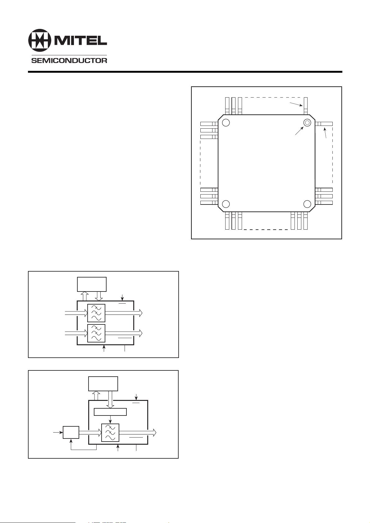
Fig. 1 A dual filter application
ADDR DATA
ADC
CLKOP
Fig. 2 Typical system application
Pin identification diagram (top view)
See Table 1 for pin descriptions and Table 2 for pinout
FEATURES
■ Sixteen MACs in a Single Device
■ Basic Mode is 16-Tap Filter at up to 40MHz
Sample Rates
■ Programmable to give up to 128 Taps with
Sampling Rates Proportionally Reducing to 5MHz
■ 16-bit Data and 32-bit Accumulators
■ Can be configured as One Long Filter or Two Half-
Length Filters
■ Decimate-by-two Option will Double the Filter
Length
■ Coefficients supplied from a Host System or a local
EPROM
■ 208-Pin Plastic PowerQuad PQ2 Package
APPLICATIONS
■ High Performance Commercial Digital Filters
■ Matrix Multiplication
■ Correlation
■ High Performance Adaptive Filtering
ORDERING INFORMATION
VP16256-27/CG/GH1N 27MHz, Commercial plastic
PowerQuad PQ2 package (GH208)
VP16256-40/CG/GH1N 40MHz, Commercial plastic
PowerQuad PQ2 package (GH208)
PIN 1
PIN 1 IDENT
PIN
208
GH208
Page 2
VP16256
Signal
DA15:0 16-bit data input bus to Network A.
DB15:0 Delayed data output bus in the single filter mode. Connected to the data input bus of the next device in a
cascaded chain. Input to Network B in the dual filter modes.
X31:0 Expansion input bus in the single filter mode. Connected to the previous filter output in a cascaded chain.
The inputs are not used on a single device system or on the Termination device in a cascaded chain. The
X bus provides the output from Network B in both dual modes.
F31:0 In single filter mode this bus holds the main device output. In dual mode it holds the output from Network␣ A.
FEN Filter enable. The first high present on an SCLK rising edge defines the first data sample. The control
register and coefficient memory must be configured before FEN is enabled. The signal must stay active
whilst valid data is being received and must be low if FRUN is high.
DFEN Delayed filter enable. This output is connected to the Filter Enable input of the next device in a cascaded
chain when moving towards the termination device and with multiple stand-alone EPROM-loaded
configurations. It is used to coordinate the control logic within each device.
SWAP Selects either the upper or lower set of coefficients for Bank Swap. A low selects the lower bank, a high
the upper bank.
FRUN In EPROM load mode, when high this signal allows continuous filter operations to occur without the need for
the initial FEN edge. If the device is not a single, interface or master device then this pin must be tied low.
DCLR A low on this signal on the SCLK rising edge will clear all the internal accumulators. DCLR need only remain
low for a single cycle, signal BUSY will indicate when the internal clearing is complete. After a clear the
device must be re-synchronised to the data stream using FEN. It is recommended that FEN is taken low
at the same time as clear. FEN may then be taken high to synchronise the data stream once BUSY has
returned low.
C15:0 16-bit coefficient input bus. In the Byte mode of operation, C15:8 have alternative uses as explained in the
text.
A7:0 Coefficient address bus. In the EPROM mode A7:0 are address outputs for an EPROM. In the remote host
mode they are inputs from the host. A7 is not used when coefficients are loaded as 16-bit words.
CCS This pin is similar in operation to A7:0 and provides a higher order address bit. When low the coefficients
are loaded, when high the control register is loaded.
WEN In the remote mode this pin is an input which when low enables the load operation. In the EPROM mode
it is an output which provides the write enable for other slave devices.
CS This pin is always an input and must also be low for the internal write operation to occur.
BYTE When this pin is tied low, coefficients are loaded as two 8-bit bytes. When the pin is high they are loaded
as 16-bit words. In the EPROM mode this pin is ignored.
EPROM When this pin is tied low coefficients are loaded as bytes from an external EPROM. The device outputs
an address on A7:0. When the pin is high coefficients must be loaded from a remote master. They can then
be transferred individually rather than as a complete set.
SCLK The main system clock; all operations are synchronous with this clock. The clock rate must be either 1, 2,
4, or 8 times the required data sampling rate. The factor used depends on the required filter length.
CLKOP This output, when used to enable SCLK, can provide a data sampling clock. It has the effect of dividing
the SCLK rate by 1, 2, 4 or 8 depending on the filter mode selected.
OEN Tri-state enable for the F bus. When high the outputs will be high impedance. OEN is registered onto the
device and does not therefore take effect until the first SCLK rising edge
BUSY A high on this signal indicates that the device is completing internal operations and is not yet able to accept
new data. The signal is used during automatic EPROM loading, reset and accumulator clearing.
RES When this pin is low the control logic and accumulators are reset. In the EPROM mode it will initiate a load
sequence when it goes high.
NOTES
1. Unused buses (e.g. X31:0 when the device is configured in single or termination mode) can be set to any value. They should however be
maintained at a valid logic level to avoid an increase in power consumption.
2. To ensure correct input voltage thresholds are maintained all the VDD and GND pins must be connected to adequate power and ground planes.
Description
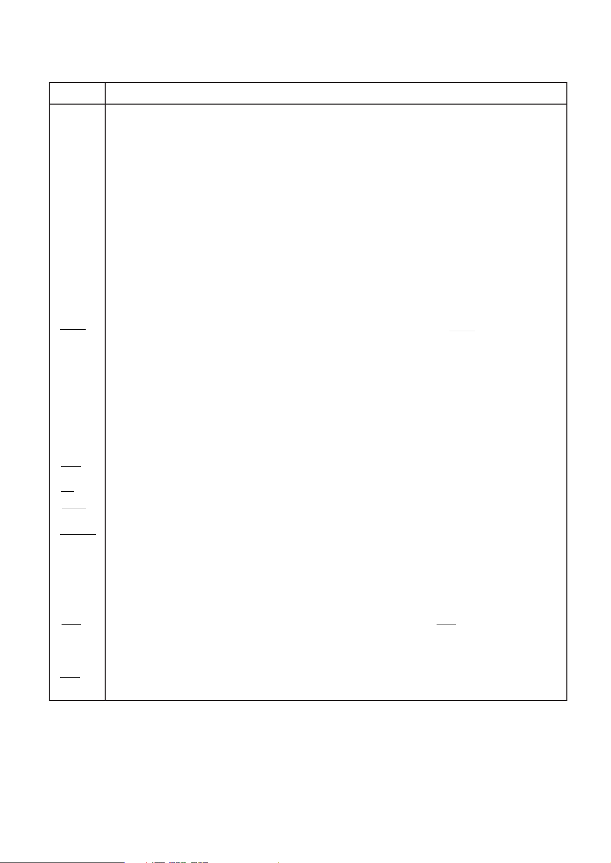
Table 1 Pin descriptions
2
Page 3
VP16256
Pin
1
2
3
4
5
6
7
8
9
10
11
12
13
14
15
16
17
18
19
20
21
22
23
24
25
26
27
28
29
30
31
32
33
34
35
36
37
38
39
40
41
42
Signal
V
DD
F0
F1
GND
F2
F3
V
DD
F4
F5
GND
F6
F7
V
DD
F8
GND
F9
F10
V
DD
F11
F12
GND
F13
F14
F15
V
DD
F16
F17
GND
F18
F19
V
DD
F20
F21
F22
F23
V
DD
F24
F25
GND
F26
V
DD
F27
Pin
43
44
45
46
47
48
49
50
51
52
53
54
55
56
57
58
59
60
61
62
63
64
65
66
67
68
69
70
71
72
73
74
75
76
77
78
79
80
81
82
83
84
Signal
F28
F29
GND
F30
F31
V
DD
FEN
DFEN
DCLR
GND
SWAP
GND
OEN
CLKOP
V
DD
DA0
V
DD
DA1
GND
DA2
V
DD
DA3
DA4
V
DD
DA5
GND
DA6
DA7
DA8
DA9
V
DD
DA10
GND
DA11
DA12
DA13
DA14
V
DD
DA15
GND
C0
C1
Pin
85
86
87
88
89
90
91
92
93
94
95
96
97
98
99
100
101
102
103
104
105
106
107
108
109
110
111
112
113
114
115
116
117
118
119
120
121
122
123
124
125
126
Signal
GND
C2
V
DD
C3
C4
C5
C6
V
DD
C7
GND
C8
C9
C10
GND
C11
C12
C13
V
DD
C14
V
DD
C15
GND
GND
WEN
CCS
CS
V
DD
RES
GND
SCLK
GND
V
DD
BYTE
EPROM
A0
V
DD
A1
GND
A2
A3
A4
V
DD
Pin
127
128
129
130
131
132
133
134
135
136
137
138
139
140
141
142
143
144
145
146
147
148
149
150
151
152
153
154
155
156
157
158
159
160
161
162
163
164
165
166
167
168
Signal
A5
A6
GND
A7
DB0
V
DD
DB1
GND
DB2
DB3
DB4
V
DD
DB5
GND
DB6
DB7
V
DD
DB8
V
DD
DB9
DB10
GND
DB11
DB12
V
DD
DB13
DB14
GND
DB15
V
DD
GND
BUSY
X0
V
DD
X1
GND
X2
V
DD
X3
X4
X5
X6
Pin
169
170
171
172
173
174
175
176
177
178
179
180
181
182
183
184
185
186
187
188
189
190
191
192
193
194
195
196
197
198
199
200
201
202
203
204
205
206
207
208
Signal
GND
X7
X8
V
DD
X9
GND
X10
X11
X12
V
DD
X13
X14
GND
X15
X16
X17
V
DD
X18
GND
X19
X20
X21
V
DD
X22
GND
X23
X24
X25
X26
GND
X27
V
DD
X28
X29
X30
GND
X31
V
DD
FRUN
GND
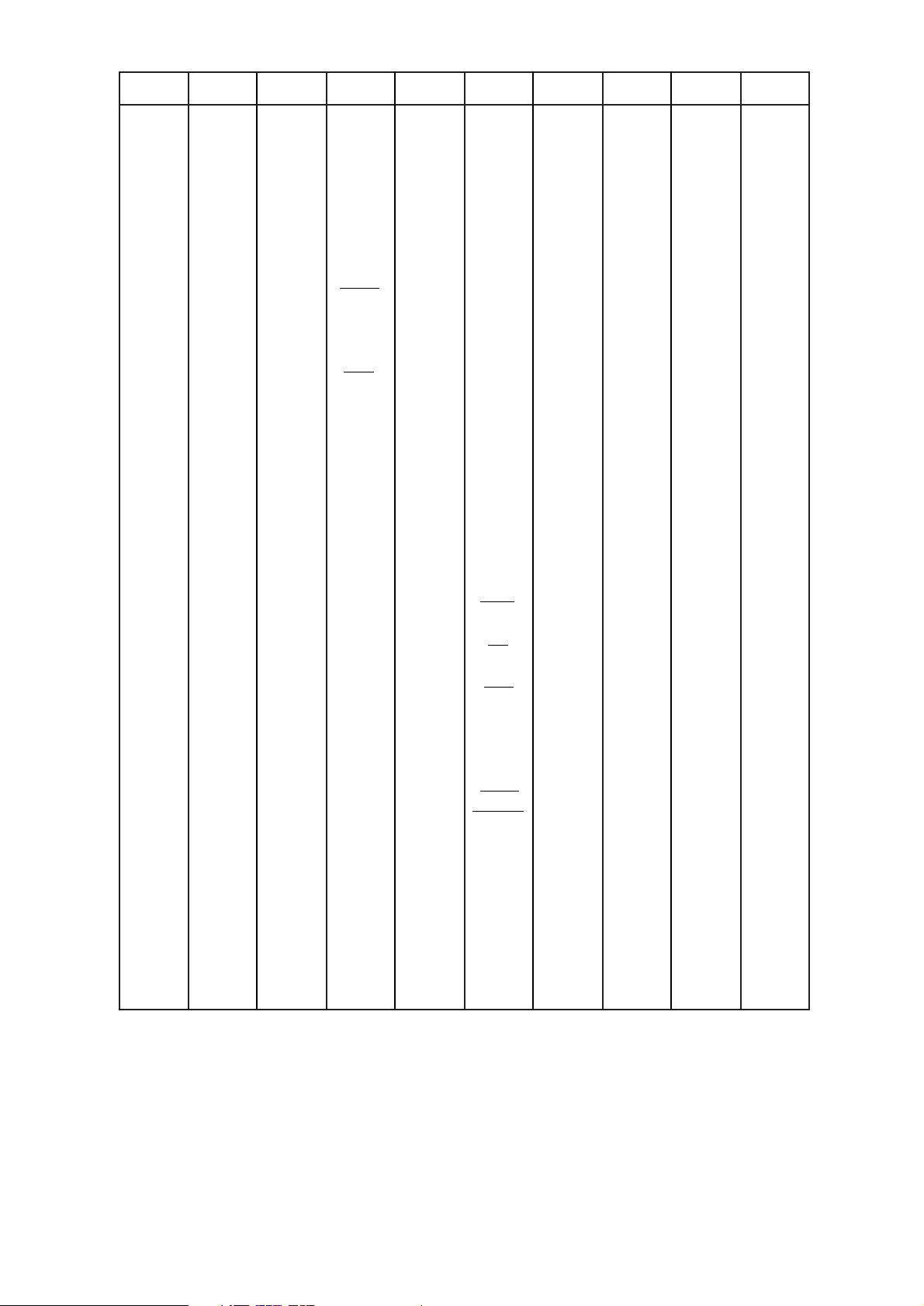
Table 2 VP16256 pinout (208-pin Power PQFP - GH208)
3
Page 4
VP16256
DA15:0 F31:0 OEN
SCLK FRUN
SWAP
A7:0
C15:0
CCS
WEN
CS
BYTE
EPROM
FEN
DFEN
DCLR
RES
COEFFICIENT
STORAGE
AND
CONTROL
CLKOP BUSY
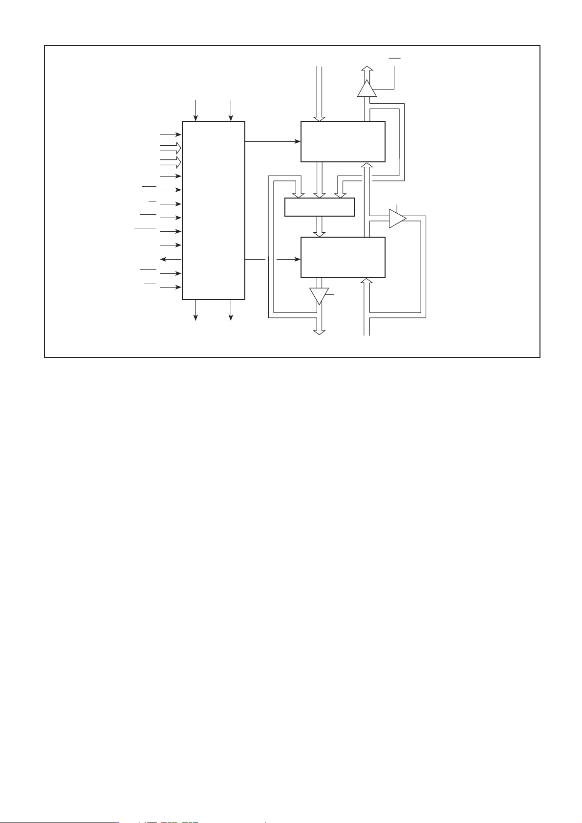
Fig. 3 Block Diagram
OPERATIONAL OVERVIEW
The VP16256 is an application specific FIR filter for use in
high performance digital signal processing systems. Sampling
rates can be up to 40MHz. The device provides the filter
function without any software development, and the options
are simply selected by loading a control register. The device
can be user configured as either a single filter, or as two
separate filters. The latter can provide two independent filters
for the in-phase and quadrature channels after IQ splitting, or
can provide two filters in cascade for greater stop band
rejection.
The device operates from a system clock, with rates up to
40MHz. This clock must be 1, 2, 4, or 8 times the required
sampling frequency, with the higher multiplication rates
producing longer filter networks at the expense of lower
sampling rates. Devices can be connected in cascade to
produce longer filter lengths. This can be accomplished
without the need for any additional external data delays, and all
the single device options remain available.
Continuous inputs are accepted, and continuous results
produced after the internal pipeline delay. Connection can be
made directly to an A-D converter. The filter operation can be
synchronised to a Filter Enable signal (FEN) whose positive
going edge marks the first data sample. The internal multiplier
accumulator array can be cleared with a dedicated input. This
is necessary if erroneous results obtained during the normal
data ‘flush through’ are not permissible in the system.
NETWORK
A
DUAL
MUX
NETWORK
B
SINGLE
MODE
DB15:0 X31:0
MODE
Coefficients can be loaded from a host system using a
conventional peripheral interface and separate data bus.
Alternatively, they can be loaded as a complete set from a byte
wide EPROM. The device produces addresses for the EPROM
and a BUSY output indicates that the transfer is occurring. Up
to sixteen devices can have their coefficients supplied from a
single EPROM. These devices need not necessarily be part of
the same filter network.
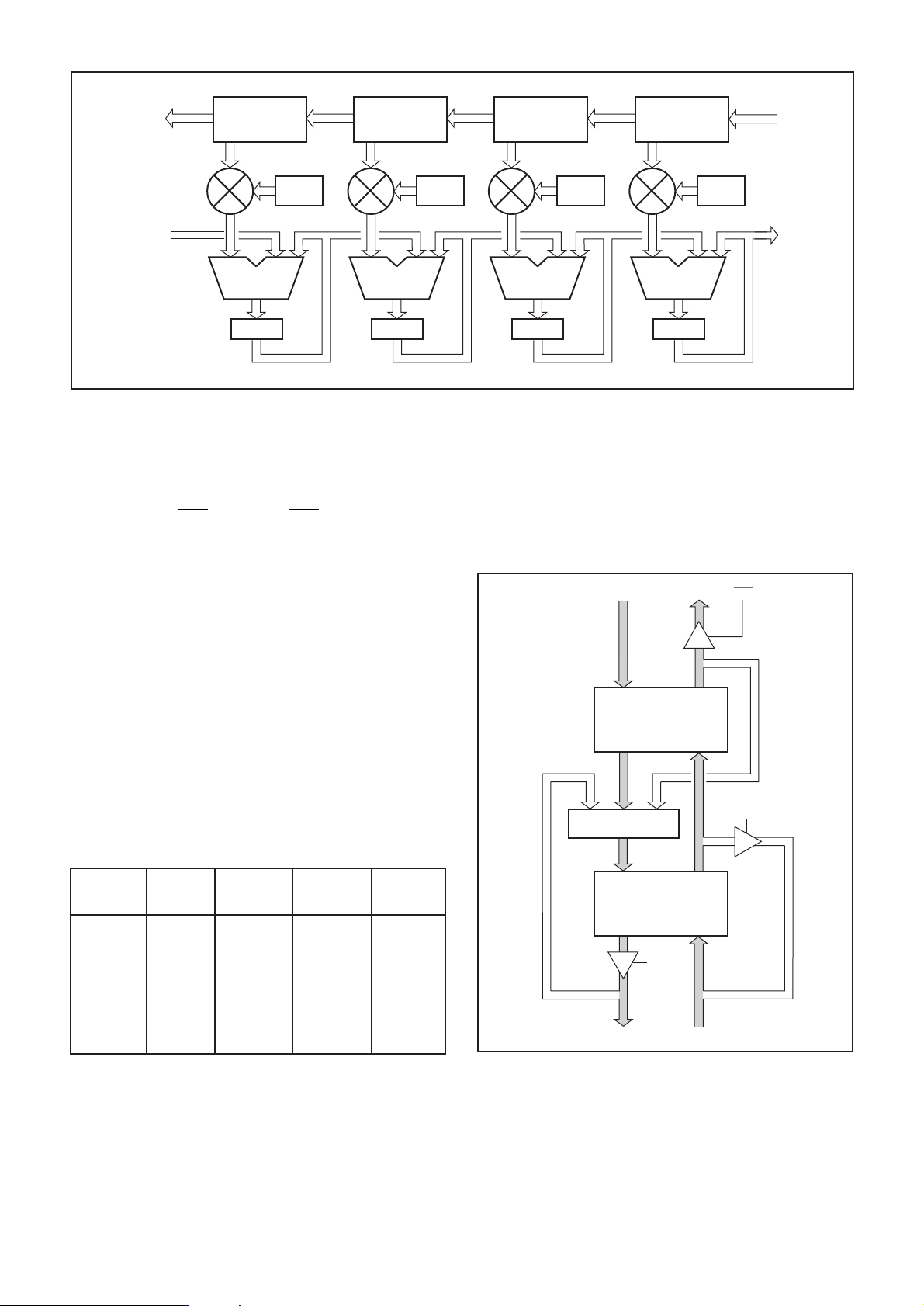
Each of the filter networks shown in Fig. 3 contains eight
systolic multiplier accumulator stages; an example with four
stages is shown in Fig. 4. Input data flows through the delay
lines and is presented for multiplication with the required
coefficient. This is added to either the last result from this
accumulator or the result from the previous accumulator. The
filter results progress along the adders at the data sample rate.
If the sample rate equals SCLK divided by four, for example,
then the accumulated result is passed onto the next stage
every fourth cycle. The structure described is highly efficient
when used to calculate filtered results from continuous input
data.
A comprehensive digital filter design program is available
for PC compatible machines. This will optimise the filter
coefficients for the filter type required and number of taps
available at the selected sample rate within the VP16256
device. An EPROM file can be automatically generated in
Motorola S-record format.
4
Page 5
VP16256
DATA
OUT
ACCUMULATE
EXPANSION
IN
DATA
DELAY LINE
ADDER
2
1
Z
COEFF
RAM
DATA
DELAY LINE
COEFF
ADDER
2
1
Z
RAM
Fig. 4 Filter network diagram
SINGLE FILTER OPTIONS
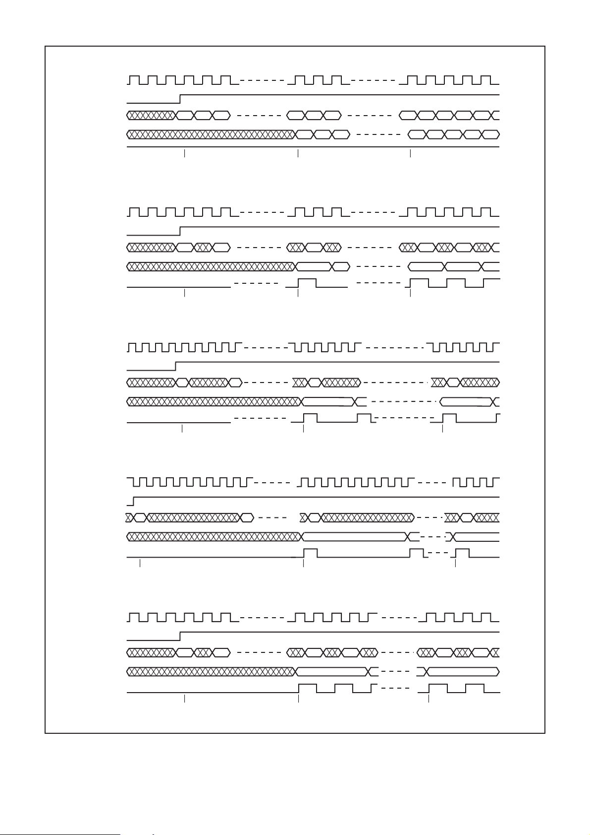
When operating as a single filter the device accepts data on
the 16-bit DA bus at the selected sample rate, see Figs. 5 and 6.
Results are presented on the 32-bit F bus, which may be
tristated using the OEN input. Signal OEN is registered onto the
device and does not therefore take effect until the first SCLK
rising edge. Devices may be cascaded this allows filters with
more taps than available from a single device. To accomplish
this two further buses are utilised. The DB bus presents the
input data to the next device in cascade after the appropriate
delay, while, partial results are accepted on the
X bus.
Single filter mode is selected by setting control register bit
15 to a one. The required filter length is then selected using
control register bits 14 and 13 as summarised in Table 3. The
options define the number of times each multiplier accumulator
is used per sample clock period. This can be once, twice, four
times, or eight times.
In addition a normal/decimate bit (CR12) allows the filter
length to be doubled at any sample rate. This is possible when
the filter coefficients are selected to produce a low pass filter,
since the filtered output would then not contain the higher
frequency components present in the input. The Nyquist
criterion, specifying that the sampling rate must be at least
double the highest frequency component, can still then be
satisfied even though the sampling rate has been halved.
DATA
DELAY LINE
COEFF
ADDER
2
1
Z
RAM
DATA
DELAY LINE
COEFF
ADDER
2
1
Z
RAM
DATA
IN
RESULT
OUT
The system clock latency for a single device is shown in
Table 3. This is defined as the delay from a particular data
sample being available on the input pins to the first result
including that input appearing on the output pins. It does not
include the delay needed to gather N samples, for an N tap filter,
before a mathematically correct result is obtained.
DA15:0 F31:0 OEN
NETWORK
A
DUAL
MUX
MODE
CR Input Output Filter Setup
14 13 12 Rate Rate Length Latency
0 0 0 SCLK SCLK 16 Taps 16
0 0 1 SCLK SCLK/2 32 Taps 17
0 1 0 SCLK/2 SCLK/2 32 Taps 16
0 1 1 SCLK/2 SCLK/4 64 Taps 18
1 0 0 SCLK/4 SCLK/4 64 Taps 20
1 0 1 SCLK/4 SCLK/8 128 Taps 24
1 1 0 SCLK/8 SCLK/8 128 Taps 24
Table 3 Single Filter options
NETWORK
B
SINGLE
MODE
DB15:0 X31:0
Fig. 5 Single Filter bus utilisation
5
Page 6
VP16256
SPEED MODE 0 (Data input and output at f
SCLK
FEN
DA15:0
F31:0
CLKOP
123
ABC
) CR14:13 = 00, CR12 = 0. CLKOP held high.
SCLK
16 17 18
First data point (A)
is read on edge 1
SPEED MODE 1 (Data input and output at half f
SCLK
FEN
DA15:0
F31:0
CLKOP
123
AB
SCLK
16 17 18
First data point (A)
is read on edge 1
SPEED MODE 2 (Data input and output at a quarter f
SCLK
FEN
DA15:0
123
AB
45 23 24
A′ B′ C′
First valid result
including data point (A)
available after edge 16
) CR14:13 = 01, CR12 = 0
A′ B′
First valid result
including data point (A)
available after edge 16
) CR14:13 = 10, CR12 = 0
SCLK
20 21 22
31 32 33
A′′ B′′ C′′
34 35
D′′ E′′
Valid result contains
the first 16 data points
available after edge 31
78 79 80
A′′ B′′ C′′
81 82
Valid result contains
the first 32 data points
available after edge 78
272 273
274 275 276
F31:0
CLKOP
First data point (A)
is read on edge 1
SPEED MODE 3 (Data input and output at an eighth f
SCLK
FEN
DA15:0
F31:0
CLKOP
SPEED MODE 1 Decimating (Data input at half f
SCLK
FEN
DA15:0
F31:0
123
A
45
First data point (A)
is read on edge 1
123
AB
6789
B
SCLK
18 19 20
A′ B′
First valid result
including data point (A)
available after edge 20
) CR14:13 = 11, CR12 = 0
SCLK
24 25 26
A′ B′
27 28
29 30 31 32
First valid result
including data point (A)
available after edge 24
and output at a quarter f
21 22
B′
SCLK
A′′ B′′
Valid result contains
the first 64 data points
available after edge 272
1040
1041 1042 1043
A′′
Valid result contains
the first 128 data points
available after edge 1040
) CR14:13 = 01, CR12 = 1.
142 143 144
B′′
145
CLKOP
First data point (A)
is read on edge 1
First valid result
including data point (A)
available after edge 18
Valid result contains
the first 64 data points
available after edge 142
Fig. 6 Single Filter timing diagrams
6
Page 7
DUAL INDEPENDENT FILTER OPTIONS
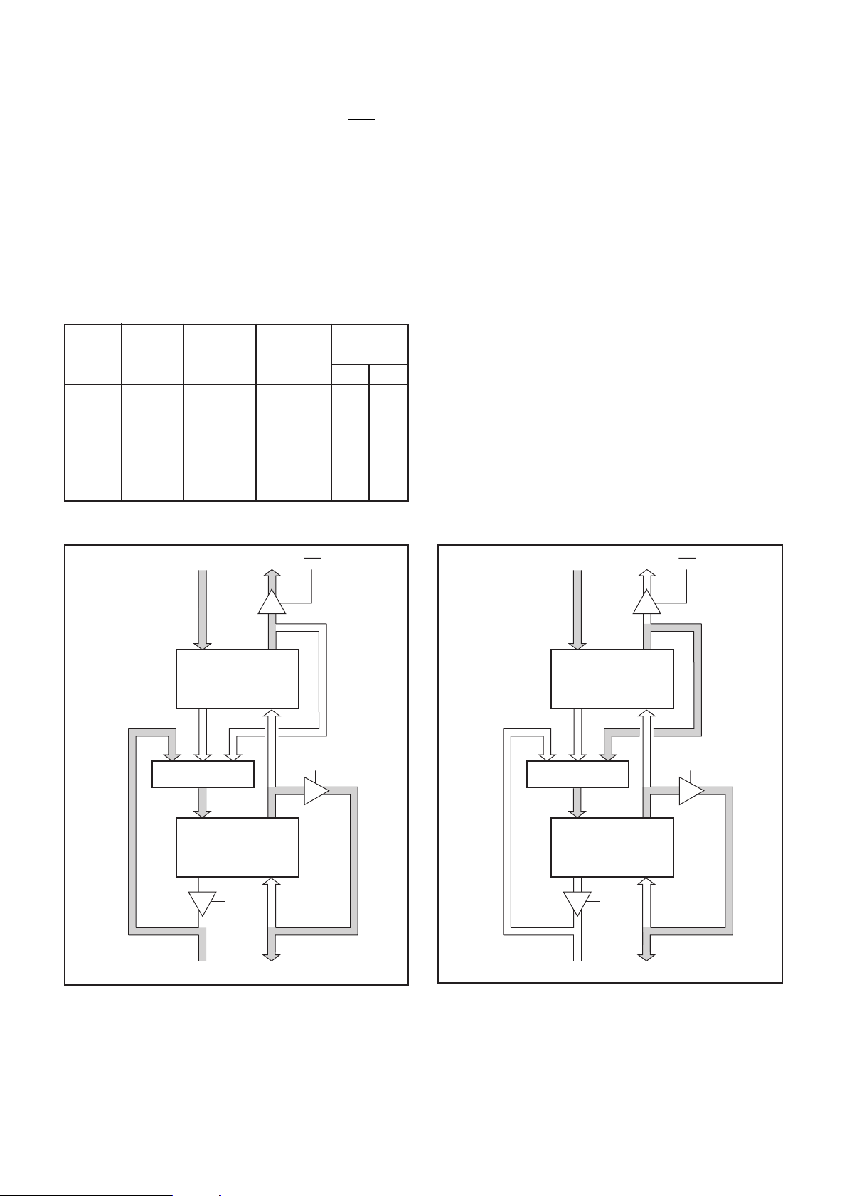
When operating as two independent filters the device
accepts 16 bit data on both the DA and DB buses at the selected
sample rate, see Fig. 7. Results are available from both the F
and X buses. The F bus may be tristated using the OEN input.
Signal OEN is registered onto the device and does not therefore
take effect until the first SCLK rising edge
Each filter must be configured in the same manner, and
multiple device expansion is not possible due to the pin re-
organization. The latter requirement can, of course, still be
satisfied by several devices configured as single filters.
Dual independent filter mode is selected by setting control
register bits 15 and 4 to a zero. The required filter length is
selected using control register bits 14 and 13 as summarised in
Table 4, which also shows the resulting latency. As in single
filter mode normal or decimate-by-two operation can be
selected using control register bit 12.
CR Input Output Filter Setup
14 13 12 Rate Rate Length Latency
Ind Cas
0 0 0 SCLK SCLK 8 Taps 16 27
0 0 1 SCLK SCLK/2 16 Taps 17 0 1 0 SCLK/2 SCLK/2 16 Taps 16 28
0 1 1 SCLK/2 SCLK/4 32 Taps 18 1 0 0 SCLK/4 SCLK/4 32 Taps 20 36
1 0 1 SCLK/4 SCLK/8 64 Taps 24 1 1 0 SCLK/8 SCLK/8 64 Taps 24 40
VP16256
DUAL CASCADED FILTER OPTIONS
When operating as two cascaded filters the device accepts
16 bit data on the DA bus at the selected sample rate. Results
are presented on the 32-bit X bus, see Fig. 8. Each filter must
be configured in the same manner. Multiple device expansion
is not possible in this mode.
Dual cascaded filter mode is selected by setting control
register bit 15 to a zero and bit 4 to a one. The required filter
length is selected using control register bits 14 and 13 as
summarised in Table 4, which also shows the resulting latency.
The decimate-by-two option is not available in this mode.
The data for the second filter network is extracted as the
middle 16 bits from the first networks accumulated result. For
successful operation the first filter network must have unity
gain. See the section on filter accuracy for more details.
The cascade option is used to increase the stop band
rejection in a practical filter application. Theoretically,
increasing the number of taps in an FIR filter will increase the
stop band rejection, but this assumes floating point calculations
with no accuracy limitations. In practice, with fixed point
arithmetic, better performance is achieved with two smaller
filters in series.
Table 4. Dual Filter options
DA15:0 F31:0 OEN
NETWORK
A
DUAL
MUX
NETWORK
B
SINGLE
MODE
MODE
DA15:0 F31:0 OEN
NETWORK
A
DUAL
MUX
NETWORK
B
SINGLE
MODE
MODE
DB15:0 X31:0
DB15:0 X31:0
Fig. 8 Dual cascaded filter bus utilisationFig. 7 Dual independent filter bus utilisation
7
Page 8
VP16256
FILTER ACCURACY
Input data and coefficients are both represented by 16-bit
two’s complement numbers. The coefficients are converted to
twelve bits by rounding towards zero. This is achieved as
follows. If the coefficient is positive then the least significant
4 bits are discarded. If the coefficient is negative then the
logical ‘OR’ of the least significant 4 bits are added to the
remainder of the word. Twelve bit coefficients can be used
directly provided the least significant four bits are set to zero.
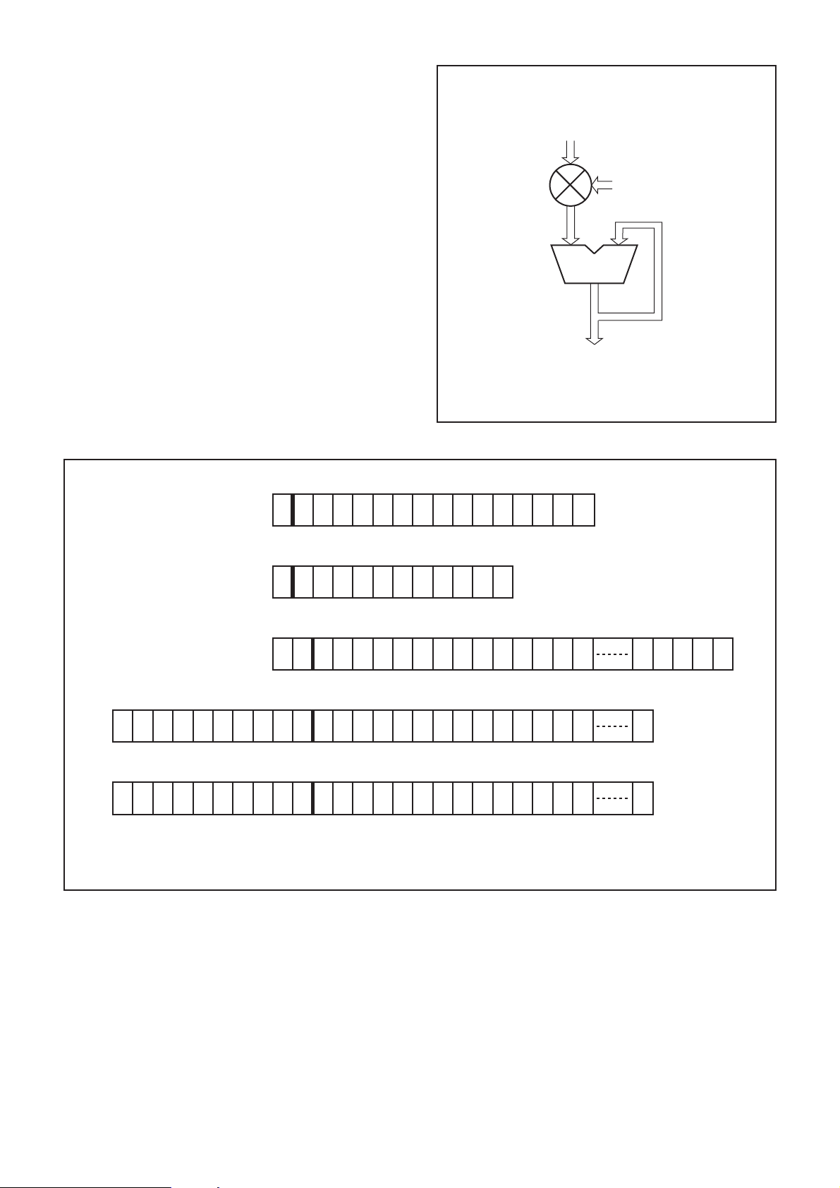
The FIR filter results are calculated using a multiplier
accumulator structure as shown in Fig. 9. The truncation and
word growth allowed for in the data path are explained in
Fig.␣ 10. The 16-bit data and 12-bit coefficient inputs (each with
one sign bit before the binary point), are presented to the
multiplier. This produces a 28-bit result with two bits before the
binary point. Producing the full 28-bit result ensures that if both
the data and coefficients are set to logic 1 a valid result is
generated. Prior to entering the accumulator the least
significant 4 bits of the multiplier result are truncated and the
resulting 24 bits sign extended to 32 bits. The final accumulator
result is 32 bits with 10 bits before the binary point. Thus 9 bits
of word growth are allowed within the accumulator. All
accumulator bits are made available on the output pins.
In cascade mode the middle 16 bits from the network A
accumulator are fed round to the network B data inputs, see
Fig. 10.
INPUT DATA
COEFFICIENT
ADDER
ACCUMULATOR
RESULT
Fig. 9 Multiplier Accumulator
INPUT DATA
COEFFICIENT
MULTIPLIER RESULT
ACCUMULATOR RESULT
S S S S S S S S S 0
ACCUMULATOR RESULT
S 8 7 6 5 4 3 2 1 0
S
S
S 0 -26
-14-13-12-11-10-9-8-7-6-5-4-3-2-1 -15
-11-10-9-8-7-6-5-4-3-2-1
Multiplication producing a 28-bit result
Sign extended to 32 bits, least significant 4 bits truncated
These bits are passed to filter network B during cascade mode
Fig. 10 Filter accuracy
-25-24-23-22-14-13-12-11-10-9-8-7-6-5-4-3-2-1
-22-14-13-12-11-10-9-8-7-6-5-4-3-2-1
-22-14-13-12-11-10-9-8-7-6-5-4-3-2-1
8
Page 9
CASCADING DEVICES
When the filter requirements are beyond the capabilities
of a single device, it is possible to connect several devices in
cascade increasing the number of taps available at the required
sample rate. Within each device all filter length, decimate, and
bank swap options are still possible, but each device in the
chain must be similarly programmed and configured as a single
filter.
The number of devices which can be cascaded is only
limited by the possibility of overflow in the 32-bit intermediate
accumulations. If more than sixteen devices are cascaded in
auto EPROM load mode, then an additional EPROM will be
needed.
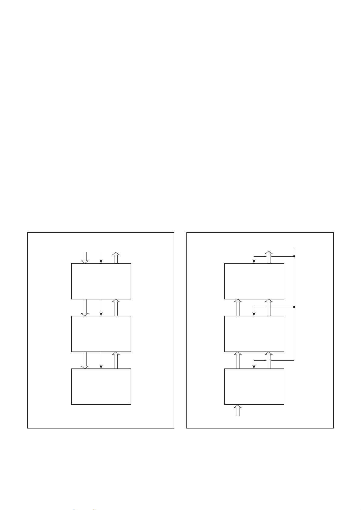
In modes where the data sample rate does not equal the
clock rate. Then the cascade arrangement shown in Fig. 11 is
used. Delayed data is passed from device to device in one
direction, while intermediate results flow in the opposite
direction. The interface device both accepts the input data and
produces the final result. It is not necessary for each device to
know its exact position in the chain, but the device which
receives the input data and produces the final result must be
identified, as must the device which terminates the chain. The
former is known as the Interface device and the latter as the
Termination device, all others are Intermediate devices.
Control Register bits CR11:10 are used to define these
positions as shown in Table 6.
The control logic in each of the devices must be
synchronised with respect to the Interface device. This is
achieved by connecting the Delayed Filter Enable output
(DFEN) to the Filter Enable input (FEN) of the next device in the
chain. The Interface device, itself, needs a FEN signal
produced by the system, unless in EPROM mode, where FRUN
VP16256
may be pulled high. Even when the latter is true, the FEN
connection must be made between the remaining devices in
the chain. By effectively extending the filter length, the cascade
latency is therefore the same as for the single device in the
same mode. Once the pipeline is initially flushed the latency is
as given in Table 3.
When devices are cascaded such that the data sample rate
equals the clock rate, (Control register bits 14:13 = 00), then a
different cascade configuration must be used. This is shown in
Fig. 12. The number of devices that can be cascaded is, again,
only limited by the 32-bit accumulators.
In this mode the delayed data is passed from device to
device in the same direction as the intermediate results. The
device which accepts the input data is now at the opposite end
of the chain to the device which produces the final result. The
control logic in each of the devices must be synchronised this
is achieved by connecting all the device FEN inputs to the
global FEN. The cascade latency for the complete filter is built
up from the 12 delays from the termination device, 8 delays
from the interface device and additional intermediate devices
each adding 4 delays.
AVAILABLE OPTIONS
No more than 128 coefficients can be stored internally. This
limits the filter length / decimate / bank swap options to those
which do not require more than that number of coefficients.
Thus when a filter with 128 taps is to be implemented in a single
device, it is not possible to decimate or bank swap. When a filter
with 64 taps is implemented, decimate or bank swap are
possible, but not both. With all other filter lengths, all decimate
and bank swap configurations are possible.
DATA IN FEN
DA15:0
DB15:0
DA15:0
DB15:0
DA15:0
DB15:0
FEN F31:0
INTERFACE
DEVICE
DFEN X31:0
FEN F31:0
INTERMEDIATE
DEVICE
DFEN X31:0
FEN F31:0
TERMINATION
DEVICE
DFEN X31:0
RESULTS
OUT
DB15:0
DA15:0
DB15:0
DA15:0
DB15:0
DA15:0
DATA IN
FEN F31:0
INTERFACE
DEVICE
DFEN X31:0
FEN F31:0
INTERMEDIATE
DEVICE
DFEN X31:0
FEN F31:0
TERMINATION
DEVICE
DFEN X31:0
OUT
FENRESULTS
Fig. 12 Full speed cascaded systemFig. 11 Three-device cascaded system
9
Page 10
VP16256
127
127
64
63
0
0
128 TAP
NO SWAP
POSSIBLE
64 TAP
FILTER B
NO SWAP
POSSIBLE
FILTER A
NO SWAP
POSSIBLE
127
64
63
127
96
95
64
63
32
31
0
0
UPPER
BANK
LOWER
BANK
B UPPER
BANK
A UPPER
BANK
B LOWER
BANK
A LOWER
BANK
127
64
63
32
31
0
(a) Single Filters
127
64
63
48
47
32
31
16
15
0
(b) Dual Filters
NOT USED
UPPER
BANK
LOWER
BANK
NOT USED
B UPPER
A UPPER
B LOWER
A LOWER
127
32
31
16
15
127
32
31
0
0
16 TAP32 TAP64 TAP
NOT USED
UPPER
BANK
LOWER
BANK
8 TAP16 TAP32 TAP
NOT USED
B UPPER
A UPPER
B LOWER
A LOWER
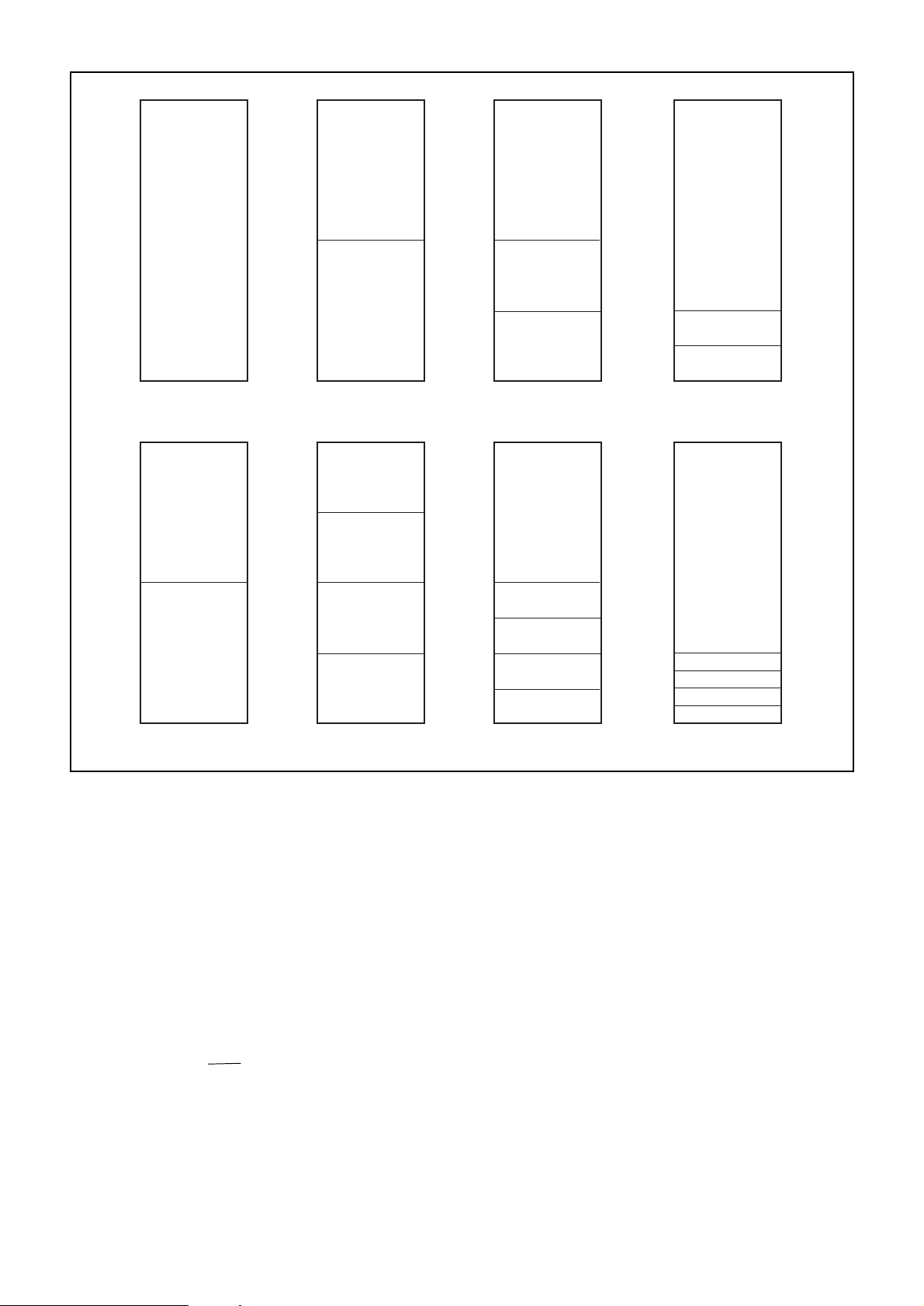
Fig. 13 Coefficient memory map
FILTER CONTROL
Two control modes are available selected by input signal
FRUN. In EPROM load mode, when FRUN is tied high the device
will commence operation once the coefficients have been
loaded. The CLKOP signal indicates when new input data is
required and that new results are available, see Fig. 6. In both
EPROM and remote master load modes, when FRUN is tied low
filter operation will not commence until a high has been detected
on signal FEN. This mode allows synchronisation to an existing
data stream. FEN should be taken high when the first valid data
sample is available so that both are read into the device on the
next SCLK rising edge.Proper device operation requires FEN to
be low during control register and coefficient loading both in
EPROM mode and Remote Master mode. After loading
coefficients, filter operation is determined by FRUN and FEN as
described above.
During device reset RES must be held low for a minimum of
16 SCLK cycles. After a reset the control register returns to its
default state of 8C80
. This places the device into the following
HEX
mode :
●
Single filter
●
Sample rate equal to the clock rate
10
●
Non-decimating
●
A single device (Not in a cascade chain)
●
Bank swap selected by bit in the control register
COEFFICIENT BANK SWAP
A Bank Swap feature is provided which allows all coefficients
to be simultaneously replaced with a different set. A bit in the
Control Register (CR7) allows the swap to be controlled by either
input signal SWAP or Control Register bit (CR6). The latter is
useful if the device is controlled by a microprocessor, when
driving a separate pin would entail additional address decoding
logic and an external latch.
If SWAP or bit CR6 is low, the coefficients used will be those
loaded into the lower banks illustrated in Fig. 13. When the
SWAP or CR6 is high, the upper banks are used.
The actual swap will occur when the next sampling clock
active going transition occurs. This can be up to seven system
clocks later than the swap transition, and is filter length
dependent. The first valid filtered output will then occur after the
pipeline latencies given in Tables 3 and 4.
By setting a bit in the Control Register it is possible to bank
Page 11
swap on every data sampling clock. This function does not
depend on the status of SWAP or bit, and the lower bank will be
initially selected after FEN goes active. The option can be used
to implement filters with complex coefficients.
LOADING COEFFICIENTS
When the device is to operate in a stand alone application
then the coefficients can be down loaded as a complete set from
a previously programmed EPROM. Alternatively if the system
contains a microprocessor they can be individually transferred
from a remote master under software control. In any mode the
system clock must be present and stable during the transfer, and
the addressing scheme is such that the least significant address
specifies the coefficient applied to the first multiplier seen by
incoming data.
The addresses used during the load operation are those
illustrated in Fig. 13. The Control Register is loaded when CCS
is high. In byte mode address A0 is used to select the portion of
control register loaded, otherwise the address bits are redundant.
VP16256
When an EPROM is used to provide coefficients, this redundancy
causes the number of locations needed for any device to be
double that for the coefficients alone.
AUTO EPROM LOAD
When EPROM is tied low, the VP16256 assumes the role of
a master device in the system and controls the loading of
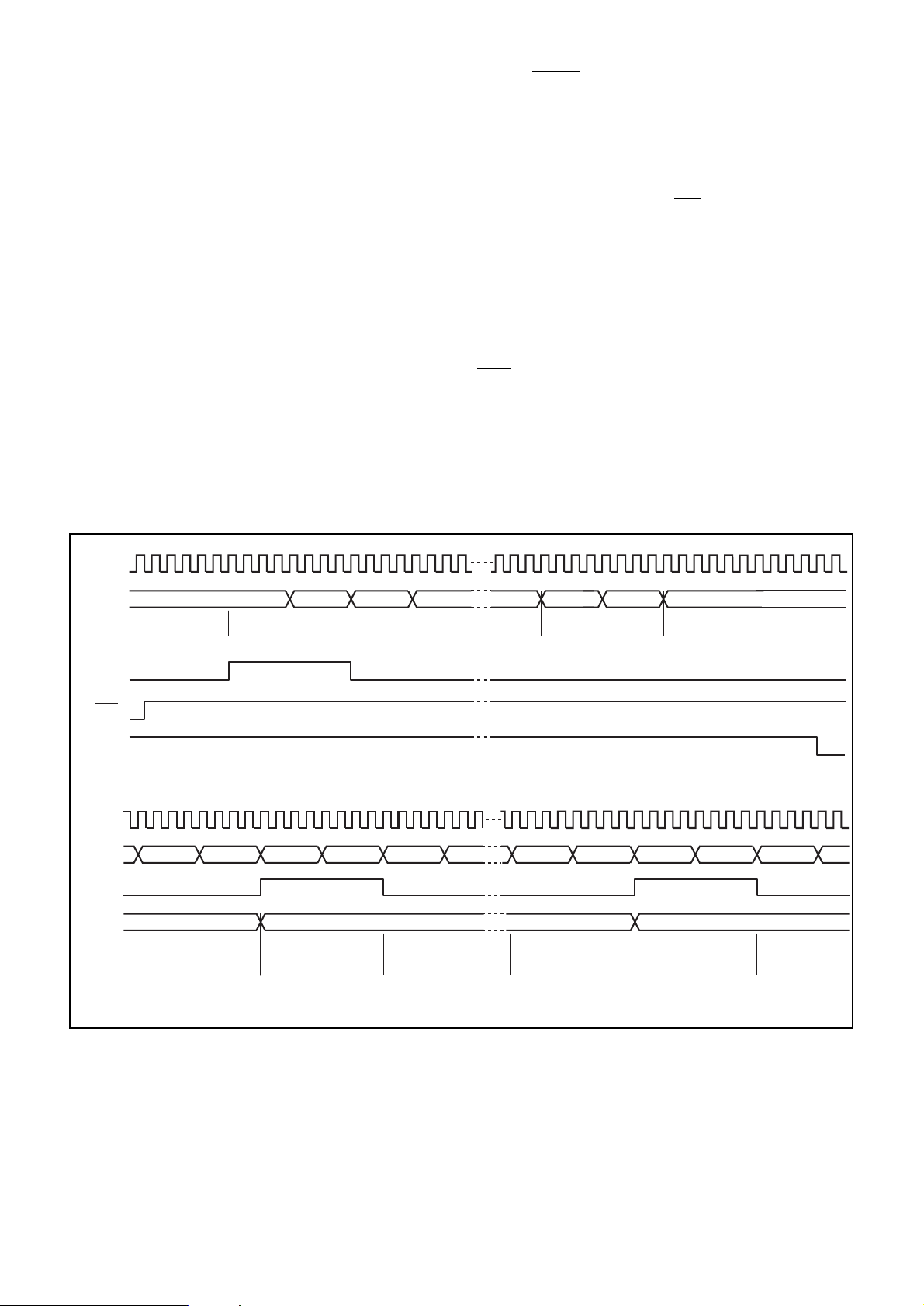
coefficients from an external EPROM, see Fig.15. A load
sequence commences when the RES input goes high, and will
continue until every coefficient has been loaded. BUSY goes high
to indicate that a load sequence is occurring and the filter output
is invalid. The device will not commence a filter operation until the
FEN edge is received after BUSY has gone low. This requirement
can be avoided if FRUN is tied high.
The address bus pins become outputs on the Master device,
and produce a new address every four system clock periods. This
four clock interval, minus output delays and the data set up time,
defines the available EPROM access time.
The coefficients are always loaded as bytes. The state of the
BYTE pin on the master device is ignored. This arrangement also
allows the eight most significant coefficient bus pins (C15:8) to be
used for other purposes as described later. Since the 16-bit
coefficients are loaded in two bytes the A0 pin specifies the
required byte. The maximum number of stored coefficients is
128, eight address outputs are therefore provided for the
EPROM. These eight outputs from the Master must also drive the
address inputs on the slave devices.
SCLK
A7:0
CCS
RES
BUSY
SCLK
A7:0
CCS
C15:12
00 01
LOAD MASTER CONTROL
REGISTER
00 01
LOAD FIRST COEFFICIENT
VALID ADDR VALID ADDR
LOAD LAST COEFFICIENT
00
Fig. 14a EPROM load sequence
FE FF 00 01 00 01 FE FF 00 01 00 01
0000 0001 0001 0010
LOAD LAST
MASTER
COEFFICIENT
LOAD SLAVE 1
CONTROL
REGISTER
LOAD SLAVE 1
COEFFICIENTS
LOAD LAST
SLAVE 1
COEFFICIENT
LOAD SLAVE 2
CONTROL
REGISTER
LOAD SLAVE 2
COEFFICIENTS
Fig. 14b EPROM load sequence for a cascaded system
Fig. 14 EPROM load sequence timing diagrams
11
Page 12
VP16256
EPROM
ADDRESS
LSB
MSB
DATA
A7:0
CCS
C15:12
C7:0
A7:0
CCS
C15:12
C7:0
A7:0
CCS
C15:12
C7:0
VP16256
MASTER
VP16256
SLAVE 1
VP16256
SLAVE 2
C11:8
CS
EPROM
BYTE
WEN
C11:8
CS
EPROM
BYTE
WEN
C11:8
CS
EPROM
BYTE
WEN
(2 SLAVES)
0010
GND
GND
GND
0001
GND
V
DD
GND
0010
GND
V
DD
GND
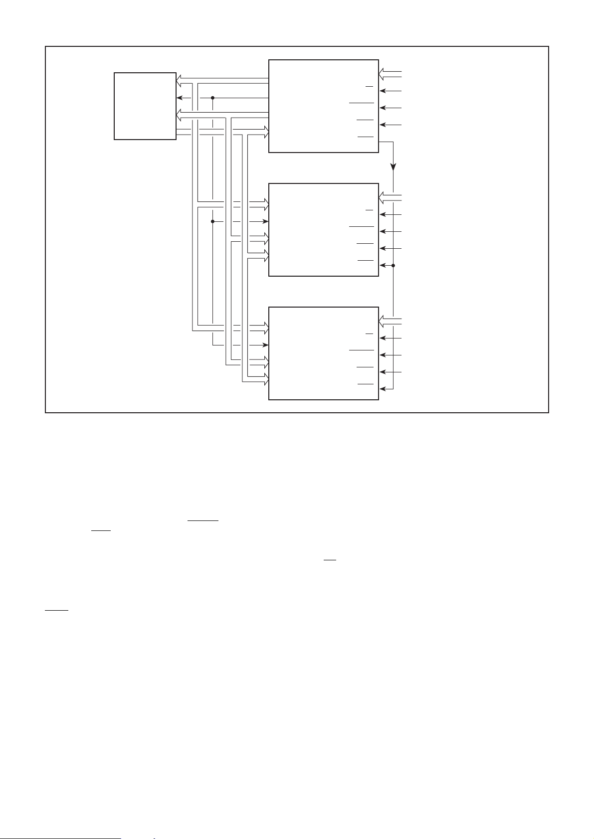
Fig. 15 Three device auto EPROM load
When the filter length is less than the maximum, the
VP16256 will only transfer the correct number of coefficients,
and one or more significant address bits will remain low.
Sufficient coefficients are always loaded to allow for a possible
Bank Swap to occur, and the EPROM allocation must allow for
this even if the feature is not to be used. Table 5 shows the
number of coefficients loaded for each of the modes.
If several devices are cascaded, only one device assumes
the role of the Master by having its EPROM pin grounded. It
produces a WEN signal for the other devices, plus four higher
order address outputs on C15:12, see Fig. 14. The extra
address bits on C15:12 define separate areas of EPROM,
containing coefficients for up to fifteen additional devices. The
least significant block of memory must always be allocated to
the Master device. The additional devices need not in practice
be all part of the same cascaded chain, but can consist of
several independent filters. They must, however, all have their
BYTE pins tied low. FRUN can still be used to start these
independent filters after all the devices have been loaded. In
this case, however, each slave FEN pin should be driven by
DFEN from the master device.
When one EPROM is supplying information for several
devices, some means of selectively enabling each additional
device must be provided. This is achieved by using the C11:8
pins on the slave devices as binary coded inputs to define one
to fifteen extra devices. These coded inputs always
correspond to the block address used for the segment of
EPROM allocated to that device. Code ‘all zeros’ must not be
used since the Master device has implied use of the bottom
segment. This is necessary since the C11:8 pins are
alternatively used on the Master device to define the number
of devices supported by the EPROM.
In addition to providing the most significant addresses to
the EPROM, the C15:12 address outputs from the master
device must also drive the C15:12 inputs on the slave devices.
These C15:12 inputs are internally compared to the C11:8
inputs to decide if that device is currently to be loaded. This
approach avoids the need for external decoders and makes
the CS input redundant. This input, however, must be tied low
on every device in an EPROM supported system.
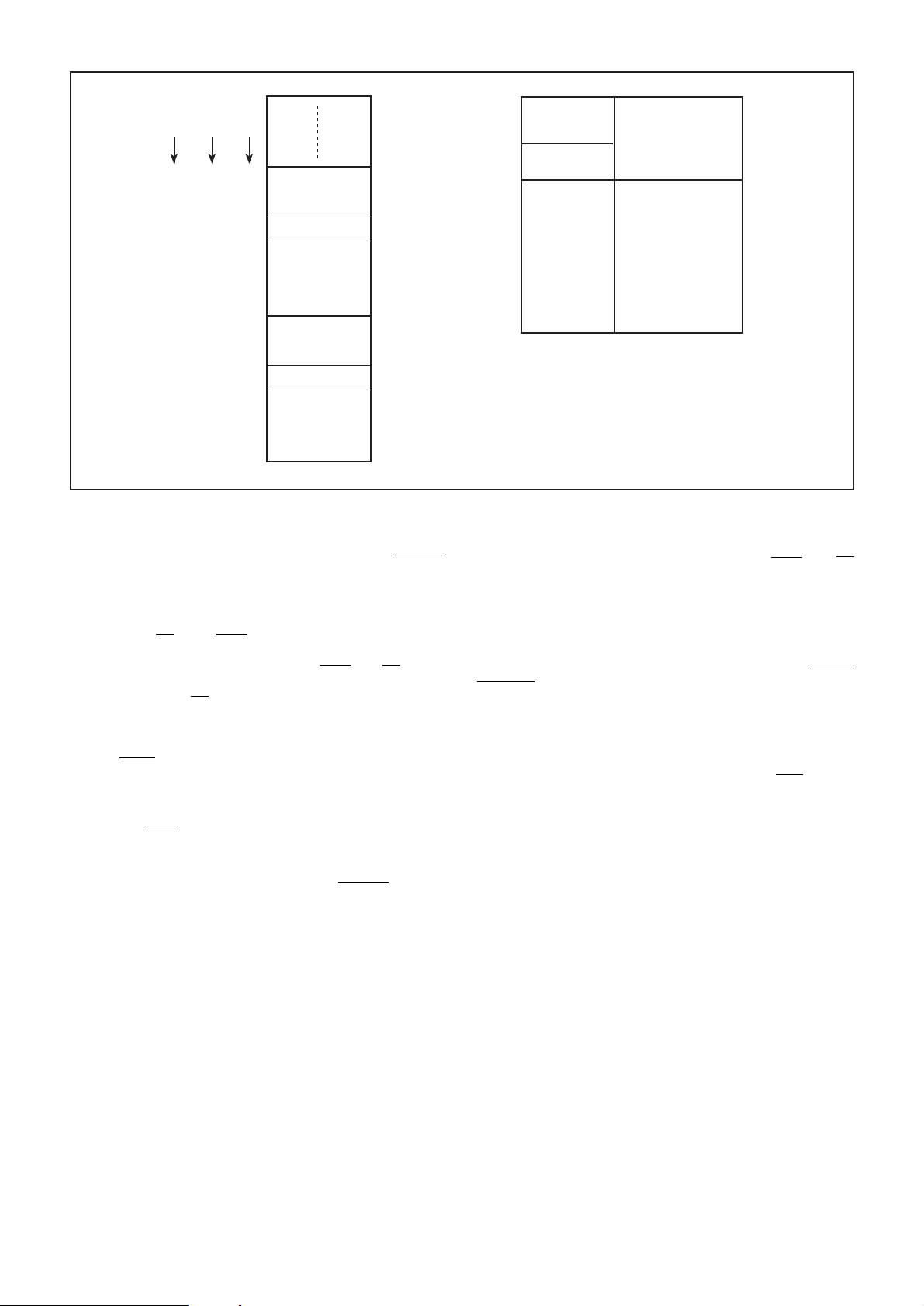
The Control Coefficient pin (CCS) is used to define when
the control register is to be loaded. It becomes an output on the
Master device which provides an EPROM address bit next in
significance above A7:0, and also drives the CCS inputs on the
slave devices. This output is high for the first two EPROM
transfers in order to access the control information, and then
remains low whilst the coefficients are loaded. This control
information is thus not stored adjacent to the coefficients within
the EPROM, and in fact the EPROM must provide twice the
storage necessary to contain the coefficients alone. All but two
of the bytes in the additional half are redundant. See Fig.16 for
the EPROM memory map.
12
Page 13
DEVICE 2
DEVICE 1
COEFFICIENTS
PER DEVICE
32 64 128
511
255
194
193
192
191
386
385
384
383
128
127
256
255
66
65
64
63
130
129
128
127
0
VP16256
Control Number of
Register Coefficients
Loaded
1023
NOT USED
770
769
CONTROL REG
768
767
FILTER
COEFFICIENTS
512
511
NOT USED
258
257
CONTROL REG
256
255
FILTER
COEFFICIENTS
0
0
NOTE:
The EPROM memory map assumes that, for the 32 and 64
coefficient per device options, the unused address pins are
unconnected. If all address pins are connected as shown in
Fig. 15 then the 128 coefficients per device memory map
column should be used. Only those coefficients required will be
read, hence the upper portions of the coefficient address space
will be ignored.
Fig. 16 EPROM Memory Map
14 13 12
000 32
001 64
010 64
0 1 1 128
1 0 0 128
1 0 1 128
1 1 0 128
1 1 1 Invalid Mode
Table 5. Number of coefficients loaded
USING A REMOTE MASTER
When a remote master is used to load coefficients, EPROM
must be tied high and a conventional peripheral interface is then
provided. It is not possible, however, to read coefficients
already stored. The master supplies an address and data bus,
and writes to the VP16256 occur under the control of
synchronous CS and WEN inputs. The Coefficient Control
Register pin (CCS) must be driven by a master address line
higher in significance than A7:0. Both the WEN and CS signals
must be low for the load operation to occur. When loading the
control register the CS signal must be held low for a further 2
cycles, see Fig. 19. Since the internal write operation is actually
performed with the system clock, it is necessary for the clock to
be present during the transfer.
The BYTE input defines whether coefficients are loaded as
a single 16 bit word or two 8-bit bytes. The latter saves on
connections to the remote master. Address bits A7:0 are used
in byte mode. 16-bit word mode uses bits A6:0, A7 being
redundant. When writing in byte mode the least significant byte
(A0 = 0) must be written first followed by the most significant
byte (A0 = 1).
In byte mode the internal comparison between C15:12 and
C11:8 is made, regardless of the state of EPROM. For this
reason pins C15:8 should all be tied low when a remote master
is used with byte transfers. This ensures that the internal
comparison gives equality and allows the load operation to
occur.
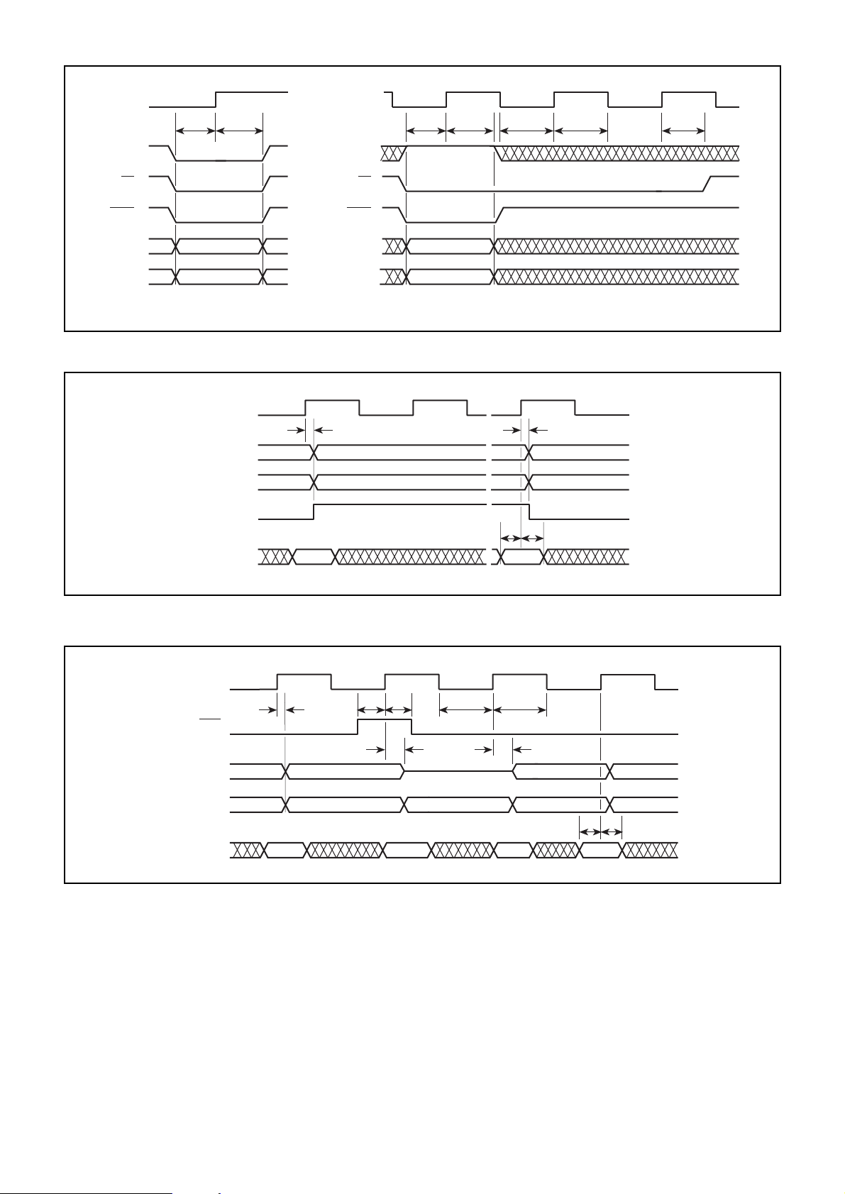
The address and coefficient buses plus the WEN and CS
signals must all meet the specified set up and hold times with
respect to the system clock, see Fig 19 and Switching
Characteristics. This synchronous interface is optimum for the
majority of high end applications, when individual coefficients
must be updated at sample clock rates. However, if the
coefficients are to be loaded under software control from a
general purpose microprocessor, the processor’s WRITE
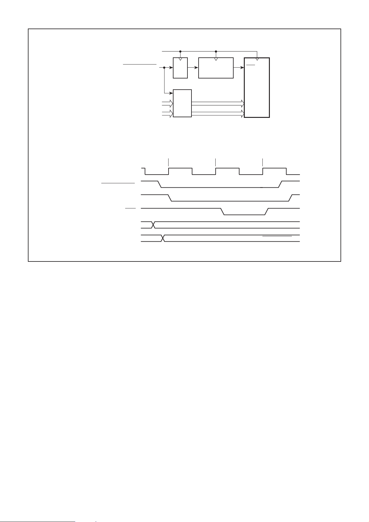
STROBE will probably be asynchronous with the SCLK clock
used by the VP16256. In this case external synchronising logic
is needed, as shown in Fig.17.
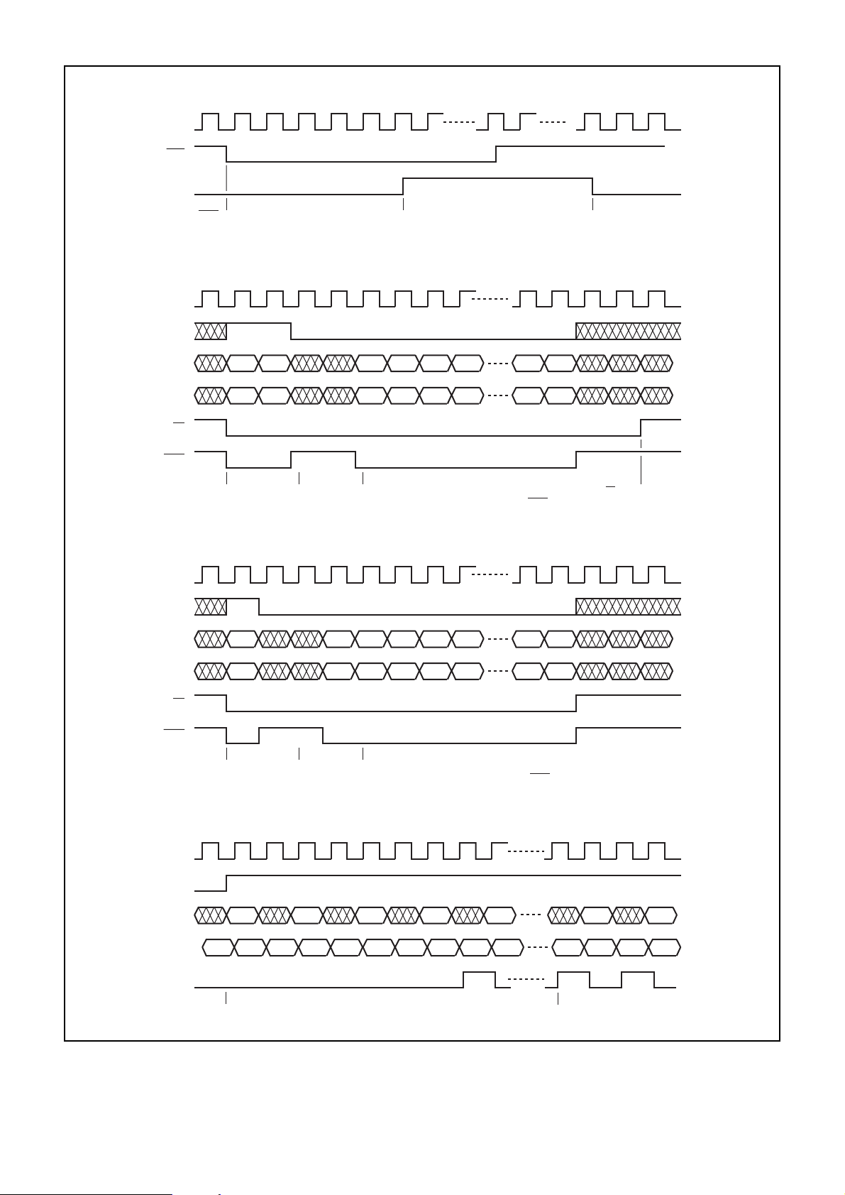
Fig. 18 shows the recommended loading sequence and
filter operation initiation. The simplest technique is to reset the
device prior to loading a set of coefficients. Coefficients may be
loaded once BUSY returns low or 22 cycles after RES is taken
high.
When loading a device from a remote master the control
register must be loaded first followed by the filter coefficients.
Fig. 18 shows the required loading sequence, two examples
are given one for byte mode the other for word mode. A gap of
at least one cycle must be left after loading the control register
before loading the first coefficient.
Filter operations are started by presenting the first data
word at the same time as raising signal FEN; FRUN should
always be low.
13
Page 14
VP16256
SCLK
PROCESSOR WRITE STROBE
SCLK
PROCESSOR WRITE STROBE
REGISTERED STROBE
VP16256 WEN
ADDRESS/DATA
A7:0/C15:0
ADDRESS
DATA
REGISTERED INTO
SYNCHRONISATION
REGISTER
DQ
COEFFICIENT
LOAD
STATE MACHINE
WEN
VP
16256
HOLD
CIRCUIT
STROBE
ADDRESS AND DATA VALID
A7:0 AND C15:0 HELD AFTER FALLING EDGE OF WRITE STROBE
STROBE
REGISTERED
INTO STATE
MACHINE
A7:0
C15:0
COEFFICIENT
INPUT CLOCKED
TO VP16256 ON
THIS EDGE
Fig. 17 Remote Master synchronisation
14
Page 15
VP16256
DEVICE RESET
1234567 1617 373839
SCLK
RES
BUSY
RES must be held low
for 16 cycles
BYTE WIDE COEFFICIENT LOAD
1234567
SCLK
CCS
A7:0
C15:0
CS
WEN
Control register loaded
with CCS high
00 01 00 01 02 03 3E 3F
00 AC 10 00 20 00 00 02
Blank cycles Coefficients loaded into the required address location.
BUSY goes active Coefficient loading may start
8 67 68 69 70 71
This example uses byte wide loading (
once BUSY has returned low
CS
BYTE
held low).
must be maintained
for two cycles
WORD WIDE COEFFICIENT LOAD
1234567
SCLK
CCS
A7:0
C15:0
CS
WEN
Control register loaded
with CCS high
00 01 02 03 1E 1F
AC00 0020 0030 0040 0050 001F 0200
00
0010
Blank cycles Coefficients loaded into the required address location.
START OF FILTER OPERATION
1234567
SCLK
FEN
DA15:0
F31:0
0010
0000
0020 0030 0040 0050 00A0
8 34 35 36 37 38
04
This example uses word wide loading (
8 916171819
BYTE
held high).
0090
0001
0001 0004 00040000 0000 0000 0000 0000 0000 0000 0000 0000
CLKOP
The first data sample
is read as FEN goes high
The first result available. CLKOP
indicates the first active result cycle
Fig. 18 Device startup timing diagrams
15
Page 16
VP16256
CONTROL REGISTER
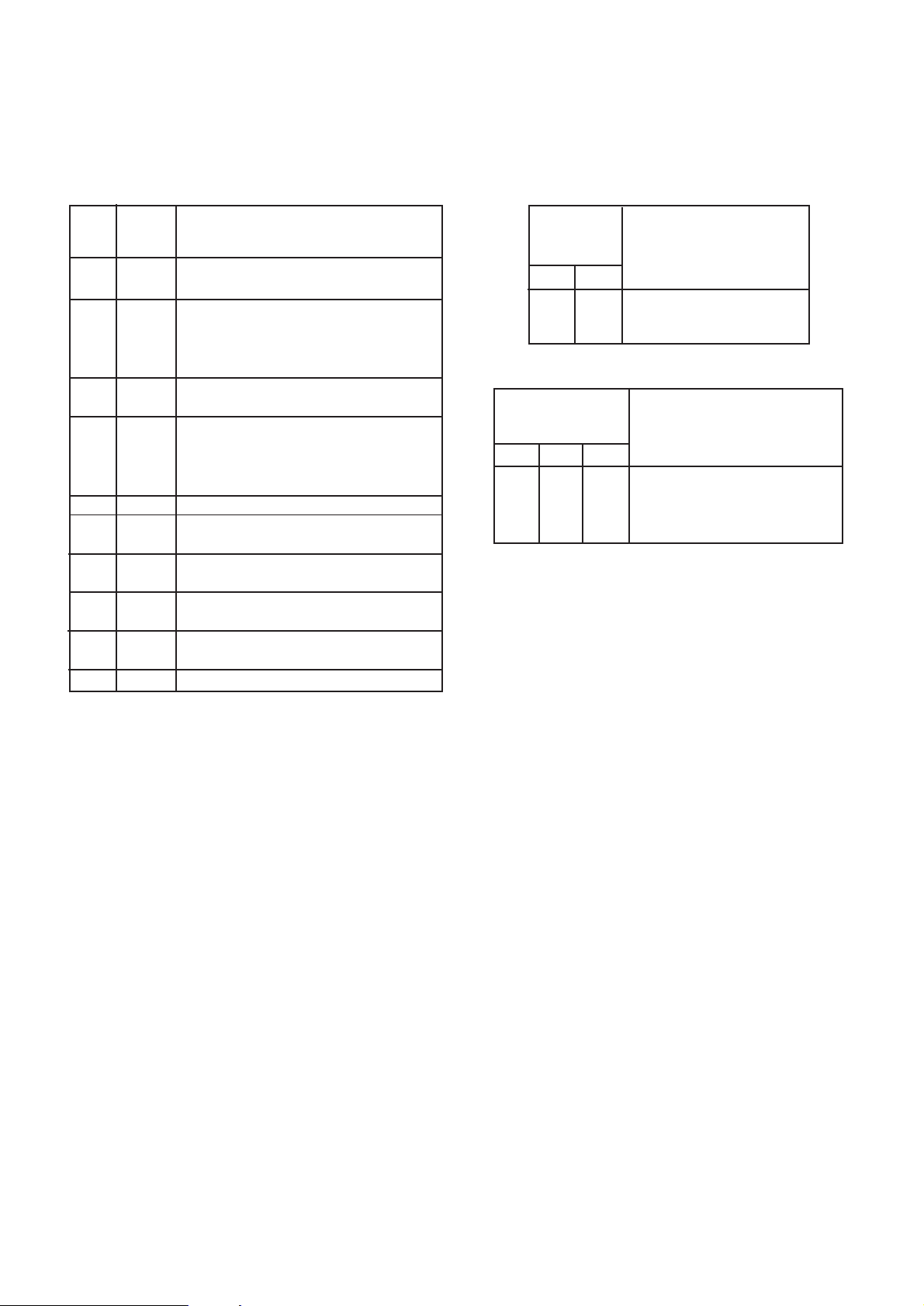
The internal operation of the VP16256 is controlled by the
status of a 16-bit control register. In the dual filter modes both
networks are controlled by the same register. The significance
of the various bits are shown in Table 6. Tables 7 and 8 define
the control register bit interdependence for the filter and bank
swapping modes.
The control register is double buffered. This allows the
writing of a new control word without affecting the current
operation of the device. To activate the new control register
after it has been written to the device the bank swap signal must
be toggled. After a reset the active control register is loaded
directly and bank swap need not be used.
Bits Decode Function
15 0 Dual filter mode
15 1 Single filter mode
14:13 00 Sample rate is the system clock
14:13 01 Sample rate is half the system clock
14:13 10 Sample rate is quarter the system clock
14:13 11 Sample rate is eighth the system clock
12 0 Output rate equals the input rate
12 1 Decimate-by-two
11:10 00 Intermediate device
11:10 01 Interface device
11:10 10 Termination device
11:10 11 Single device
9:8 00 These bits MUST be at logical zero
7 0 Bank swap is controlled by input pin
7 1 Bank swap is controlled by Bit 6
6 0 Lower bank if bit 7 is set
6 1 Upper bank if bit 7 is set
5 0 Normal Bank Swap
5 1 Bank swap on every sample clock
4 0 Two independent filters
4 1 Two filters in cascade
3:0 These bits MUST be at logical zero
Control
Register Function
Bits
15 4
0 0 Two independent filters
0 1 Two filters in cascade
1 X Single Filter
Table 7 Control register filter mode bits
Control
Register
Bits
Function
765
0 X 0 Control by input pin
1 0 0 Lower bank selected
1 1 0 Upper bank selected
X X 1 Swap on every sample clock
Table 8 Control register bank swap bits
Table 6 Control register bit allocation
ABSOLUTE MAXIMUM RATINGS (Note 1)
Supply voltage V
Input voltage V
Output voltage V
Clamp diode current per pin I
Static discharge voltage (HBM) 500V
Storage temperature T
DD
IN
OUT
S
(see note 2) 18mA
K
Ambient temperature with power applied T
Junction temperature with power applied T
20·5V to 17·0V
20·5V to VDD 10·5V
20·5V to VDD 10·5V
265°C to1150°C
0°C to170°C
AMB
J
120°C
Package power dissipation 2500mW
Thermal resistance, junction-to-case θ
JC
1·0 °C/W
NOTES
1. Exceeding these ratings may cause permanent damage.
Functional operation under these conditions is not implied.
2. Maximum dissipation should not be exceeded for more
than1 second, only one output to be tested at any one time.
3. Exposure to absolute maximum ratings for extended
periods may affect device reliablity.
4. Current is defined as negative into the device.
5. The θ
data assumes that heat is extracted from the
JC
bottom of the package via the integral heat sink.
6. The metal ‘heat slug’ in the base of the package is
connected to the substrate, which is at V
potential.
DD
16
Page 17
VP16256
SCLK
CCS
CS
WEN
C15:0
A7:0
t
VALID ADDRESS
HS
VALID DATA
t
HH
(a) Coefficient Write
SCLK
A7:0
C15:12
CCS
C7:0
SCLK
t
CL
CCS
CS
WEN
C15:0
A7:0
t
VALID ADDRESS
HS
VALID DATA
t
HH
(b) Control Register Write
Fig. 19 Remote Master setup and hold timings
∼
CLK 1 CLK 2 CLK 9
t
CD
VALID ADDRESS
VALID ADDRESS
∼
∼
∼
∼
∼
∼
∼
∼
∼
∼
∼
tHSt
∼
∼
HH
∼
∼
t
CH
t
CD
t
HH
SCLK
OEN
F31:0
OUTPUT PINS
INPUT PINS
Fig. 20 EPROM load timings
t
t
OS
t
CD
VALID DATA
VALID DATA VALID DATAVALID DATA
OH
t
CZF
HIGH Z
Fig. 21 Operating timings
t
CL
t
CH
t
VALID DATA
CVF
tHSt
HH
17
Page 18
VP16256
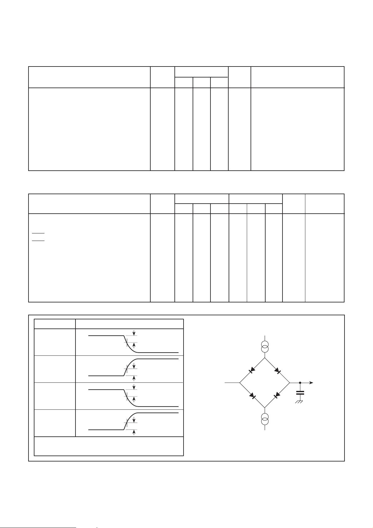
ELECTRICAL CHARACTERISTICS
The Electrical Characteristics are guaranteed over the following range of operating conditions, unless otherwise stated:
T
= 0°C to 170°C, TJ = 1120°C, VDD = 15V±10%, GND = 0V
AMB
Static Characteristics
Characteristic
Output high voltage
Output low voltage
Input high voltage (CMOS)
Input low voltage (CMOS)
Input high voltage (TTL)
Input low voltage (TTL)
Input leakage current
Input capacitance
Output leakage current
Output short circuit current
Symbol
V
OH
V
OL
V
IH
V
IL
V
IH
V
IL
I
IN
C
IN
I
OZ
I
OS
Switching Characteristics (see Figs. 19, 20 and 21)
Characteristic Symbol
Input signal setup to clock rising edge
Input signal hold after clock rising edge
OEN set up to clock rising edge
OEN hold after clock rising edge
Clock rising edge to output signal valid
Clock frequency
Clock high time
Clock low time
Clock to data valid F bus from high impedance
Clock to data high impedance F bus
V
current
DD
NOTE 1. VDD = 15·5V, outputs unloaded, clock frequency = Max.
t
HS
t
HH
t
OS
t
OH
t
CD
f
SCLK
t
CH
t
CL
t
CVF
t
CZF
I
DD
Value
Min. Typ. Max.
2·4
-
3·5
-
2·0
-
210
-
0·4
-
1·0
-
0·8
110
10
250
10
150
300
VP16256-27
Min. Typ. Max.
8
0
20
4
5
14
14
-
-
290
-
-
-
18
27
-
35
35
325
Units
V
IOH = 4mA
V
I
= 4mA
OH
V
SCLK input only
V
SCLK input only
V
All other inputs
V
All other inputs
µA
GND < V
pF
µA
GND < V
mA
VDD = 15·5V
VP16256-40
Min. Typ. Max.
7
0
20
4
5
10
10
-
-
395
-
-
-
17
40
-
23
23
450
Conditions
< V
IN
DD
< V
OUT
DD
ns
ns
ns
ns
ns
MHz
ns
ns
ns
ns
mA
ConditionsUnits
30pF
See Fig. 22
See Fig. 22
See Note 1
Test Waveform measurement level
Delay from
output high
V
H
0·5V
to output
high impedance
Delay from
output low
to output
high impedance
Delay from
output high
1·5V
V
L
0·5V
0·5V
impedance to
output low
Delay from
output high
impedance to
output high
is the voltage reached when the output is driven high
V
H
VL is the voltage reached when the output is driven low
1·5V
0·5V
Fig. 22 Three state delay measurement
18
I
OL
1·5V
I
OH
Three state delay measurement load
DUT
30pF
Page 19
Page 20

http://www.mitelsemi.com
World Headquarters - Canada
Tel: +1 (613) 592 2122
Fax: +1 (613) 592 6909
North America Asia/Pacific Europe, Middle East,
Tel: +1 (770) 486 0194 Tel: +65 333 6193 and Africa (EMEA)
Fax: +1 (770) 631 8213 Fax: +65 333 6192 Tel: +44 (0) 1793 518528
Fax: +44 (0) 1793 518581
Information relating to products and services furnished herein by Mitel Corporation or its subsidiaries (collectively “Mitel”) is believed to be reliable. However, Mitel assumes no
liability for errors that may appear in this publication, or for liability otherwise arising from the application or use of any such information, product or service or for any infringement of
patents or other intellectual property rights owned by third parties which may result from such application or use. Neither the supply of such information or purchase of product or
service conveys any license, either express or implied, under patents or other intellectual property rights owned by Mitel or licensed from third parties by Mitel, whatsoever.
Purchasers of products are also hereby notified that the use of product in certain ways or in combination with Mitel, or non-Mitel furnished goods or services may infringe patents or
other intellectual property rights owned by Mitel.
This publication is issued to provide information only and (unless agreed by Mitel in writing) may not be used, applied or reproduced for any purpose nor form part of any order or
contract nor to be regarded as a representation relating to the products or services concerned. The products, their specifications, services and other information appearing in this
publication are subject to change by Mitel without notice. No warranty or guarantee express or implied is made regarding the capability, performance or suitability of any product or
service. Information concerning possible methods of use is provided as a guide only and does not constitute any guarantee that such methods of use will be satisfactory in a specific
piece of equipment. It is the user’s responsibility to fully determine the performance and suitability of any equipment using such information and to ensure that any publication or
data used is up to date and has not been superseded. Manufacturing does not necessarily include testing of all functions or parameters. These products are not suitable for use in
any medical products whose failure to perform may result in significant injury or death to the user. All products and materials are sold and services provided subject to Mitel’s
conditions of sale which are available on request.
M Mitel (design) and ST-BUS are registered trademarks of MITEL Corporation
Mitel Semiconductor is an ISO 9001 Registered Company
Copyright 1999 MITEL Corporation
All Rights Reserved
Printed in CANADA
TECHNICAL DOCUMENTATION - NOT FOR RESALE
 Loading...