

Page 1
VP2614
VP2614
H.261 Video De-Multiplexer
Supersedes version in June 1995 Digital Video & DSP IC Handbook, HB3923-2 DS3735 - 3.2 October 1996
FEATURES
■ Fully integrated H.261 video de-multiplexer
■ Inputs an H.261 bitstream. Outputs error corrected run
length coded coefficients.
■ Interfaces directly to the VP2615 H.261 decoder
■ Extracts side information and status for transfer to a
System Controller
■ User definable system level options for proprietary ap-
plications
■ Average input rates between 40 Kbit /sec and 2Mbit /
sec. Maximum peak input rates of 4 Mbit / sec.
■ 100 pin quad flatpack
ASSOCIATED PRODUCTS
■ VP2611 H.261 Encoder
■ VP2612 H.261 Video Multiplexer
■ VP2615 H.261 Decoder
DESCRIPTION
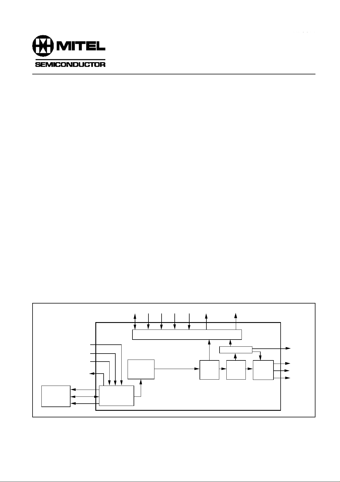
The VP2614 Video De-Multiplexer forms part of the Mitel
Semiconductor chip set for video conferencing, video telephony, and multimedia applications. It extracts video parameters and run length coded DCT coefficients from an
H.261 bitstream. Elements of the data which have been
variable length coded according to the specification are decoded within the device. It produces tagged data, aligned to a
macroblock timing structure, in the format needed by the
VP2615 Decoder. Side information and status bits are separately made available for the system controller.
The VP2614 will accept data up to a peak rate of 4 Mbits
per second, but with an average rate up to 2 Mbits per second.
The bursty nature of the input, together with the fact that each
coded picture does not use the same number of bits, requires
the provision of a received data buffer. Since the VP2615
Decoder accepts macroblock data as it becomes available, it
is not necessary to provide storage for a complete coded
picture. Worst case analysis has shown that a buffer size of
256K bits is adequate in practice for bit rates up to 2Mb/sec.
The incoming sequence is coded with a strict syntax, and
the VP2614 must identify and align with this sequence before
correct decoding is possible. Storage for this alignment is
contained within the external buffer. The device monitors that
lock is always valid, and reports to the system controller. Error
correction bits are ignored.
■ VP520S CIF / QCIF Converter
■ VP510 Colour Space Converter
DATA
STROBE
DATA
VALID
NOT
READY
RECEIVE
BUFFER
32K X 8
CNTRL
DATA
ADDR
BUFFER
INTERFACE
HD7:0 HA3:0 CEN WR RD VMUX ERROR VMUX EVENT
HOST INTERFACE
SIDE INFORMATION
FRAME
ALIGNMENT
VALIDITY
CHECK
VARIABLE
LENGTH
DECODE
Fig 1 : Simplified Block Diagram
VP2615
INTER
FACE
VP2614
PMD
2:0
D7:0
DM3:0
DCLK
1
Page 2

VP2614
PIN DESCRIPTION
SIG TYPE FUNCTION
LD I Line input data
LEN I When low, the line input data is valid.
LCLK I Line input strobe
LRED O When low, line data cannot be ac
cepted.
DBUS7:0 O Data and control bus to the VP2615.
DMODE3:0 O These outputs identify the data on
DBUS7:0.
PM2:0 O Identifiers for the additional information
on DBUS7:0 .Not used by the VP2615.
DCLK O Continuous O/P strobe for the DBUS7:0
bus which is derived from SCLK.
SCLK I System clock. Must be 27 MHz for 30 Hz
frame rates.
HD7:0 I/O Bi-directional data bus.
HA3:0 I Four system controller address bits.
WR I An active low write strobe from the
system controller.
RD I An active low read strobe from the
system controller.
CEN I An active low chip select from the sys
tem controller.
ERR O An active low output which Indicates
framing and decoding errors.
EVT O An active low output which Indicates
that new picture status data is available.
B7:0 I/O Bi-directional data bus to the receive
buffer.
A14:0 O Address bus to the receive buffer.
WS O An active low write strobe for the receive
buffer.
BCS O An active low select for the receive
buffer.
BEN O An active low output enable for the
buffer.
TCK I JTAG test clock
TMS I JTAG mode select
TDI I JTAG I/P data
TDO O JTAG O/P data
TRST I JTAG reset
TOE I When low all outputs are high imped-
ance
RES I An active low power on reset
OPERATION OF THE MAJOR BLOCKS
FRAME ALIGNMENT
The H.261 continuous bitstream is split into frames of 512
bits the first bit in each frame being part of an 8 bit frame
alignment pattern. Only the sequence in the pattern is important and detection can start from any bit. To avoid false
detection within the actual data, this pattern must be repeated
at least three times before " frame lock " can be considered to
have been achieved.
The detection of frame lock thus requires data from 24
consecutive 512 bit frames, and a section of the Received
Data Buffer is reserved for this purpose. This external RAM is
supported by a small internal buffer which allows eight consecutive bits ( obtained from reading a byte ) to be simultaneously checked for alignment with the corresponding bits in
seven other bytes spaced apart by complete frames. The
search for alignment over 512 bits takes less than 250
microseconds with a 27 MHz clock, this being less than the
time taken to receive 512 bits at the maximum rate of 2Mb/
second. Thus the buffer area for frame lock does not overflow.
Once frame lock has been achieved it is continually
monitored using the appropriate bit in each frame. If a mismatch occurs then the next four frame alignment bits will be
checked for errors. If any one of these four bits is also in error
then loss of frame alignment is declared by setting a Status
Register Bit, and a search for a new alignment position will
commence. If none are in error then a random bit error is
assumed and no further action is taken.
The check done on loss of alignment is a compromise
between falsely believing that alignment has been lost and not
detecting that frame alignment has been lost. The probability
of two random bit errors in the five frames used in the check
is dependent on the bit rate and also the error rate. With a high
error rate of 1:100000, and a bit rate of 2Mb/sec, false
detection is possible once per week. The probability of detecting a change in the frame alignment ( caused by switching in
a new bitstream ) is 46.9% in the first five frames, but this rises
to 97.4% after 12 frames have been processed.
Control Bits allow H261 framing to be either identified or
ignored. In the latter case Frame Lock will always be indicated
and data is still buffered and processed. The datastream is
then expected to contain pure data and a search will be made
to find picture start codes. When framing is enabled the 18
parity bits are extracted from the data, but single bits in error
can still go un-detected in some circumstances.
NOTE:
"Barred" active low signals do not appear with a bar in the
main body of the text.
2
Page 3
VP2614
VIDEO LOCK
Once the VP2614 has locked to the H261 frames it will
begin searching for the 20 bit unique Picture Start Code. Once
this has been identified the "Video Lock" status bit will be set,
and the bitstream will be translated on a code by code basis.
Video lock will be lost and translation process interrupted
under the following conditions:
1) A Picture Start Code or Group of Blocks ( GOB ) Start
Code is not present when expected.
2) The codeword is not valid for its context, causing no
match to be obtained. Each variable length code in the
bitstream is analysed by the VP2614, and invalid patterns will
force Video Lock to be lost.
3) Too many coefficients are transferred for the current
macroblock because the End of Block code was missing.
4) GOB number is not in the correct range for the operating mode.
5) A GOB number not in sequence will cause lock to be
lost and then regained.
Note that only the most frequently occurring coefficients
are variable length coded, the others being represented by an
escape sequence followed by a fixed length code. The Intra
DC coefficient is also a fixed length code. These fixed length
codes have bit patterns which are forbidden in the H.261
specification, but they could appear due to bit errors. These
invalid codes are trapped by the VP2614, but do not cause
Video Lock to be lost. Instead the run length coefficient is
replaced by a default value of magnitude 1. When video lock
has been lost the DMODE 3:0 outputs indicate a WAIT state.
When lock is regained any missing macroblocks are replaced
with Fixed Macroblocks.
A count is maintained of up 256 occurrences of faults 1 3, and a status bit is set when lock is lost ( the Video Lock
Achieved bit is also cleared ). An output signal is also provided
which can, if required, be used to interrupt the system controller. This indicates any of the above errors which cause Video
Lock to be lost and also frame alignment errors; alternatively
it can be used to just indicate framing errors.
When Video Lock has been achieved, the detection of a
Picture or GOB start code when it is not expected will not
cause lock to be lost. Instead the VP2614 will resynchronize
to the new start code, and dummy macroblocks will be
generated for the missing GOB's. These dummy blocks will be
Fixed Macroblocks, and will cause the VP2615 Decoder to
use data from the previously decoded picture. Note that Video
LINE
STROBE I/P
(LCLK)
LINE I/P
DATA
DATA
ENABLE (LEN)
NOT
READY O/P
(LRED)
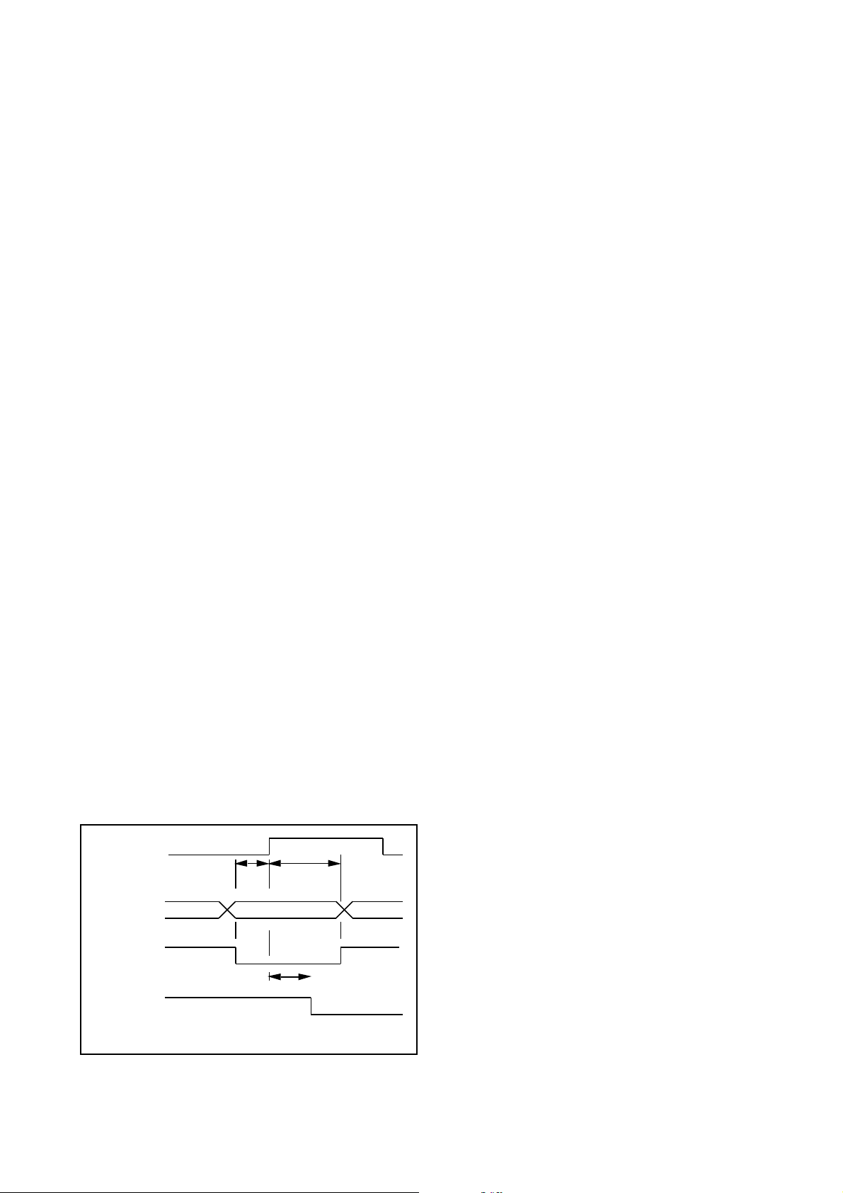
Fig 2 : Line Interface Timing
0ns
2Ø +10ns
min
Note. Ø is the system clock period
min
DATA VALID
Asynchronous
Lock is actually lost and re-gained under these conditions. The
status bit will momentarily be set and then reset, and the Video
Lock Lost Counter will be incremented.
Similarly any errors in the actual GOB number will not
cause lock to be lost and then gained again. Since sequential
GOB numbers are always produced by the encoder, then the
Decoder generates its own GOB numbers and ignores those
in the bitstream.
A Control Bit allows the system controller to take one of two
actions when Video Lock is lost. Either the VP2614 can be
forced to re-initialize to the next Picture Start Code, or it can
abandon the decoding operation until the next GOB Start
Code is detected. When lock has been lost, and a new start
code has been found, the VP2614 assumes its number to be
initially correct and starts its own sequence from that number.
If, however, the next number in the bitstream is not in sequence then this new number is used to start a new sequence.
This process continues until two sequential numbers are
obtained, and then no further checks on the GOB numbers are
made until Video Lock is again lost. The VP2614 will generate
"Fixed Macroblocks " for the missing GOB numbers since
Video Lock was lost, and will output these to the VP2615
decoder. This then uses data from the previous decoded
picture for those macroblocks.
A Video Hold bit is provided in one of the System Control
Registers which forces Video Lock to be lost immediately. No
further data is passed to the VP2615 whilst this bit is set, but
the Received Data Buffer is not allowed to fill unnecessarily.
Incoming data will be flushed out and lost. When the hold bit
is cleared a Picture Start Code must be detected to re-gain
Video Lock. The VP2615 will then be provided with any
missing GOB's as described above, before GOB's in the new
picture are processed.
A Freeze Frame Control Bit is also provided. This has a
similar action to the Video Hold Bit, except that it is only
actioned when PTYPE has been decoded in the picture layer,
and it also sets a Freeze Frame status bit. If Video Lock is lost
before the start of a new frame then Freeze Frame will become
active and a search will commence for a picture start code.
Even though Freeze Frame causes Video Lock to be lost, the
VP2614 will still search for picture start codes and will extract
PTYPE and Temporal Reference values.
If clear, a Release Mode Control Register Bit will allow the
freeze condition to be released when the Freeze Bit is cleared,
but is only actioned when the next Picture Header is decoded.
If the Release Mode Bit is set, then the freeze condition is only
released when the PTYPE bit in the H.261 stream specifies
that this is to occur. Even when automatic release has been
selected the system controller can still monitor the length of
time that the freeze has been in effect. It can then force a
release after a time out period by setting the Release Mode Bit
and clearing the Freeze Bit.
DE-MUX CORE
Once Video Lock has been achieved, the core of the
VP2615 will convert the H.261 bitstream into video parameters and run length coded coefficients. A state machine,
which is a hardware manifestation of the H.261 coding structure, maintains the current position in the bitstream. When
necessary variable length de-coding is performed, and side
information such as temporal reference and Picture Type
Information is stored in registers.
3
Page 4
VP2614
SCLK
ADDRESS
O/P
CHIP ENABLE/
O/P ENEBALE
DATA I/P
ADDRESS
O/P
CHIP
ENABLE
DATA
O/P
WRITE
ENABLE
20ns
max
20ns max
ADDRESS VALID
Tac
READ CYCLE
WRITE CYCLE
20ns
max
10ns
min
DATA VALID
VALID
20ns
max
0ns
min
20ns
max
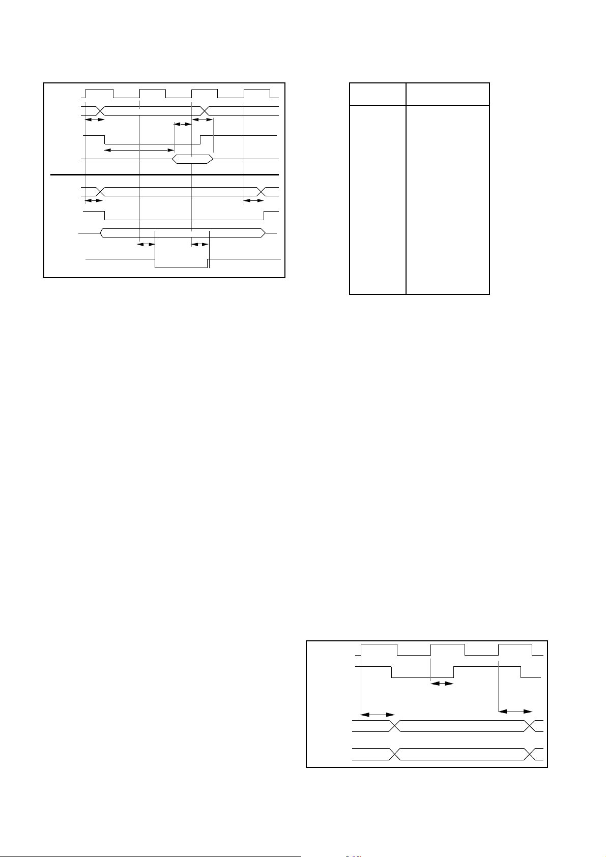
Fig 3 : External Buffer Timing
Not all this side information is used by the VP2615 Decoder, but is still made available on the data output bus
DBUS7:0. This is described in the section on Additional
Information. In addition the side information can be examined
by the system controller.
Requirements for the complete decoder system are such
that it is desirable for the VP2614 /15 pair to free run, and to
ignore the Temporal References embedded in the video
bitstream. The pair then always process the bitstream, whenever code bits are available, using the processing rate needed
for the full 30 Hz frame rate. Operating in this manner allows
the de-mux core to be closely coupled to the VP2615 Interface
circuitry, and no additional buffering is necessary. The demultiplexing process is then locked to the macroblock timing
structure needed by the VP2615.
LINE INTERFACE
Bitstream inputs to the device are controlled by an asynchronous line input strobe, which when data is valid is enabled
by a Data Valid signal. Detailed timing information is given in
Figure 2.
Maximum input frequency is 4 MHz and the rising edge of
the strobe is used to internally latch the data. The VP2614
generates a Ready signal which goes invalid when data
cannot be accepted. This, for example, occurs during system
reset or if the Received Data Buffer overflows.
EXTERNAL BUFFER REQUIREMENTS
The external buffer must be a 32K x 8 bit static RAM, and
must comply with the timing requirements given in Figure 3.
Under normal operating conditions the buffer will not overflow,
however it is conceivable that under some unforseen condition the buffer may fill and then overflow. For this reason a
Buffer Full Flag is provided in one of the Status Registers. This
is asserted when the buffer is 90% full, and is not itself an error
condition. If the buffer continues to fill and eventually overflows, then the Ready Signal to the line interface goes invalid.
The effect of overflow is to also clear the buffer and the Buffer
Empty Flag will be raised. There is no status bit to indicate
overflow, but an extended period of Buffer Full followed by
Buffer Empty can be used to infer the condition.
4
DMODE3:0 FUNCTION
0000
0001
0010
0011
0100
0101
0110
0111
1000
1001
1010
1011
1100
1101
1110
1111
GOB Number
MB Number
Control Decisions
Quant Value
Horizontal MV
Vertical MV
Coded Blk Pattern
Sub-Block No
Zero Run Count
RLC Coefficient
Not used
Not used
Not used
Not used
Not used
Wait State
Table 1. Output Codes
VP2615 INTERFACE
The VP2614 provides a glueless interface to the VP2615
Decoder. Run length coded coefficients and control information are transmitted over the DBUS7:0 bus, and are identified
by the code on the DMODE3:0 bus given in Table 1. The
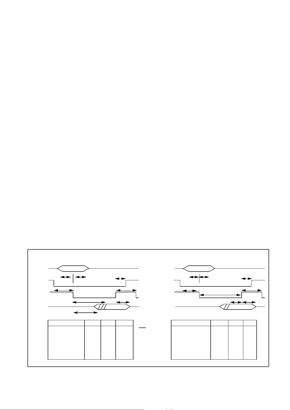
VP2614 produces a continuous DCLK which is used to strobe
data into the VP2615. This is derived by dividing the system
clock by two, and when no data is actually available the
DMODE3:0 bus will indicate a wait state. Timing is shown in
Figure 4.
The VP2615 expects a macroblock and its control information to be transferred over a minimum period, nominally
equivalent to 2048 system clock cycles but with allowance for
the asynchronous DCLK. Wait states are thus inserted as
necessary by the VP2614 in order to enforce this macroblock
period. Under normal circumstances the VP2614 will not take
longer than 2048 clock periods to produce a macroblock, but
some 10% extra time is available for each macroblock before
the 30 Hz frame rate becomes impossible to maintain.
The start of a macroblock transfer is identified by the
presence of the Control Decisions Byte ( DMODE3:0 = 0010).
Each macroblock slot must at least consist of this Control
Decisions Byte, followed by the GOB number and then the
Macroblock number. No further bytes are mandatory.
When high, Bit 0 in the Control Decisions Byte indicates a
Fixed Macroblock, and a high on Bit 1 indicates Inter Mode
coding. A high on Bit 2 indicates that the macroblock was
filtered, and a high on Bit 3 indicates that Motion Compensa-
SCLK
DCLK
O/P
25ns max
25ns max
DATA FROM
VP2614
DMODE
3:0
25ns max
DATA VALID
DATA VALID
Fig 4 : Output Timing
Page 5
VP2614
tion was used. When Bit 7 is high this indicates that CIF
resolution is in use, but the VP2615 does not use this information. Instead the host controller must supply this information.
The VP2615 is essentially a Macroblock Processor which
produces decoded data for the position on the screen defined
by the GOB and Macroblock number. Since the H.261 specification allows macroblocks to be skipped, then the VP2614
generates dummy Fixed Macroblocks if necessary ( see
below ) which are still separated by 2048 clock cycles.
Similarly after Video lock has been re-gained the VP2614 will
generate Fixed Macroblocks for those missing in the sequence, even if this wraps around into the next picture.
These steps ensure that a complete picture, containing
dummy data when necessary, is always supplied by the
VP2614. The Fixed Macroblock bit in the Control Decisions
Byte is set when dummy data is needed, and Intra Mode
decoding is specified. This causes the VP2615 to output
macroblock data from the previously decoded picture, which
was already in the frame store.
ADDITIONAL INFORMATION
Picture Type, PSPARE and GSPARE information is not
used by the VP2615 decoder. In future or proprietary uses of
H.261 this information could become considerable and be
useful to other devices in the system. This can conveniently be
supplied by using the DBUS7:0 bus when the DMODE3:0 bus
indicates that a wait state is present and there is no useful
information for the VP2615. An additional control bus PM2:0
defines the additional information that is present, with the
coding given below:
PM2:0 ADDITIONAL PARAMETER
000 Temporal Reference
001 GSPARE transfer
010 PSPARE transfer
011 PTYPE transfer
100 Quantizer step value
111 Data present is that defined by DMODE3:0
SYSTEM CONTROLLER INTERFACE
A conventional microprocessor interface is used consisting of a byte wide bi-directional data bus, four address bits, a
chip enable and separate read and write strobes. Detailed
timing is given in Figure 5.
In addition two outputs are available which can be used as
interrupts if necessary. These can be disabled by control bits.
When the Error Interrupt Source Bit is set, the ERROR signal
indicates that an error has occurred in the FEC frame alignment module. The Frame Lock Lost Status Bit is also set. The
output signal is cleared by reading the status register and will
be set again when frame alignment is again achieved. If the
host has forced a loss of alignment then ERROR does not go
active when lock is lost, but it will still go active when lock is regained.
When the Error Interrupt Source Bit is cleared, then the
ERR output also goes active when Video Lock is lost. Reading
the Status Register will detemine the actual cause of the ERR
interrupt.
The EVT signal allows the controller to synchronize with
picture related parameters extracted from the bitstream. It
goes active when new picture status data is available, as does
the Picture Ready bit in Status Register A. This bit and the
output signal are cleared when any Status Register is read.
The pipeline delay of two macroblock periods through the
VP2615 decoder will give the controller time to react to
changes in PTYPE affecting the final output of the picture in
question. When PTYPE specifies a change between CIF and
QCIF, the controller has an amount of time equivalent to that
needed to decode the first GOB before it needs inform the
VP2615 of the change in operation.
The addresses and functions of the various control and
status registers are given below. Setting a Control Bit always
performs the function specified, and a high in a Status Register indicates the state is true. All error counters saturate at their
maximum values, and are prevented from changing whilst
being read.
ADDRESS
CHIP
SELECT
READ
STROBE
DATA
OUT
READ CYCLE
Tah
Tas
Trs
CHARACTERISTIC
Addresss Set Up Time
Address Hold Time
Cip Select Set Up Time
Chip Select Hold Time
Strobe In active Time
Data Access Time
Delay to O/P's low Z
Delay to O/P's high Z
Tac
Tlz
SYMBOL
Tas
Tah
Trs
Tsh
Tri
Tac
Tlz
Thz
MIN
10ns
10ns
10ns
2ns
Øns
6Øns
Tsh
Tri
Thz
Data Valid
MAX
10 +7Øns
25ns
25ns
NOTE
Ø is the period of the
input clock
Fig 5 : Host Controller Timing
ADDRESS
CHIP
SELECT
WRITE
STROBE
DATA
IN
CHARACTERISTIC
Addresss Set Up Time
Address Hold Time
Chip Select Set Up Time
Chip Select Hold Time
Strobe In active Time
Strobe Active Time
Data Set Up Time
Data Hold Time
Tws
Tas
WRITE CYCLE
Tah
SYMBOL
Tas
Tah
Tws
Tsh
Twi
Twa
Tds
Tdh
Twa
Tds
Data Valid
MIN
10ns
10ns
10ns
2ns
3Øns
2Øns
10ns
10ns
Tsh
Twi
Tdh
MAX
5
Page 6

VP2614
SUPPLEMENTARY NOTE:
To avoid problems with register loading, the VP2614 requires
two write operations with no read strobe in between. The
absence of chip enable with the read strobe does not prevent
this problem. Thus if I/Os are memory mapped it will be
necessary to externally gate the read strobe with chip enable
for the VP2614 and to do two writes for every load operation.
STATUS REGISTER A ( ADDRESS 0 )
BIT FUNCTION
0 GSPARE Byte Available ( FIFO not Empty )
1 Freeze Frame
2 Buffer Full
3 Buffer Empty
4 Picture Information Ready
5-7 Unassigned
STATUS REGISTER B ( ADDRESS 1 )
BIT FUNCTION
0 Frame Lock Lost
1 Frame Lock Achieved
2 Video Lock Lost
3 Video Lock Achieved
4 -7 Unassigned
CONTROL REGISTER A ( ADDRESS 2 )
BIT FUNCTION ( when the bit is set )
0 Freeze Frame released by bit stream
1 Force Freeze Frame
2 Error interrupt only from Frame Lock
3 Enable EVT Interrupt
4 Enable ERR Interrupt
5 Video Hold
6 Clear Buffer
7 System Re-start
CONTROL REGISTER B ( ADDRESS 3 )
BIT FUNCTION ( when the bit is set )
0 Re-lock to Picture Start Code
1-2 Unassigned
4 000 FEC Framing Off
5:3 101 FEC Framing On
6 Clear Video Lock Lost Counter
7 Clear other Counters apart from above
Note: Control Register B must be loaded with the required
values before Register A is programmed.
USER READABLE COUNTERS
ADDRESS FUNCTION
4 FEC Frame Count
5 Filled Frames Count
9 Video Lock Lost Count
6
PICTURE STATUS REGISTERS
10 Temporal Reference Register
11 Picture Information ( see below )
12 First PSPARE Byte
13 Second PSPARE Byte
14 Top of GSPARE Stack
PICTURE INFORMATION REGISTER ( ADDRESS 11)
BIT FUNCTION
7 PSPARE Byte 2 Valid (cleared by reading byte)
6 PSPARE Byte 1 Valid (cleared by reading byte)
5 Split screen
4 Document camera
3 Freeze frame
2 CIF/QCIF
1:0 Set to one
[Bit 0 is LSB]
A master - slave arrangement is used for the Picture
Status Registers, and the slave is not updated for the duration
of the host read operation plus 32 system clock cycles.
Reading any of the counter values ( address 4-9 ) or any
Picture Status Register ( address 10-13 ) causes all values in
the respective blocks to be frozen for 32 clocks, thus allowing
a complete snapshot to be taken of the respective values.
Two bytes of PSPARE data are stored and further bytes
will be lost. Note that the VP2612 Video Multiplexer presently
only provides one byte of PSPARE information. A FIFO is
provided to provide storage for 12 GSPARE bytes, and a
status bit is provided to indicate that this FIFO is not empty,
and that the byte at the top of the stack should be read.
RESET OPERATION
In addition to the hardware reset there are several soft-
ware reset options which are selective in their action. The
hardware reset input will initialize all the internal circuit blocks,
and will clear all status registers, error counters, and address
pointers. The bits in Control Registers A and B are cleared
except that the Video Hold Bit in Register A is set, and Bits 0,4,
and 5 are set in Register B. The device will thus re-lock to a
Picture Start Code, will correct 2 bit errors, and FEC Framing
will be on. The circuit which interfaces to the VP2615 Decoder
is reset to the end of picture condition ( Macroblock 33 in GOB
12 ).
The System Re-start bit ( Bit 7 in Control Register A ) will
clear all status bits and will initialize the bitstream decoder, the
forward error corrector, and the buffer alignment modules. It
should be used if there has been an interruption in the
bitstream, and does not affect the circuit producing GOB's and
macroblocks for the VP2615 Decoder. Thus, after the re-start,
Video Lock can be obtained on a GOB boundary, and Fixed
macroblocks can be generated for missing macroblocks within
the same picture.
The Clear Buffer bit ( Bit 6 in Control Register A ) will reset
the read and write address pointers for the external buffer. A
full software restart requires both Bit 7 and Bit 6 to be set.
Two bits are also provided in Control Register B for reset
operations. One will clear the Video Lock Lost counter, the
other clears the FEC frame counter, the Filled Frames counter, and the three error counters in the error detection circuit.
Page 7

VP2614
JTAG Test Interface
The VP2614 includes a test interface consisting of a
boundary scan loop of test registers placed between the pads
and the core of the chip. The control of this loop is fully JTAG/
IEEE 1149-1 1990 compatible. Please refer to this document
for a full description of the standard.
The interface has five dedicated pins: TMS, TDI, TDO,
TCK and TRST. The TRST pin is an independent reset for the
interface controller and should be pulsed low, soon after
power up; if the JTAG interface is not to be used it can be tied
low permanently. The TDI pin is the input for shifting in serial
instruction and test data; TDO the output for test data. The
TCK pin is the independent clock for the test interface and
registers, and TMS the mode select signal.
TDI and TMS are clocked in on the rising edge of TCK, and
all output transitions on TDO happen on its falling edge.
1
2
3
4
5
6
7
8
9
FUNC
N/C
N/C
N/C
TOE
N/C
DMODE0
DMODE1
DMODE2
DMODE3
GND
VDD
DBUS0
DBUS1
DBUS2
DBUS3
DBUS4
DBUS5
DBUS6
DBUS7
VDD
PIN
21
22
23
24
25
26
27
28
29
30
31
32
33
34
35
36
37
38
39
40
FUNC
GND
DCLK
LD
PM0
PM1
PM2
N/C
N/C
N/C
N/C
HA0
HA1
HA2
HA3
SCLK
GND
VDD
HD0
HD1
HD2
PIN
41
42
43
44
45
46
47
48
49
50
51
52
53
54
55
56
57
58
59
60
PIN
10
11
12
13
14
15
16
17
18
19
20
Instructions are clocked into the 8 bit instruction register
(no parity bit) and the following instructions are available.
Instruction Register Name
( MSB first )
11111111 BYPASS
00000000 EXTEST (No inversion)
10XXXXXX INTEST (Product test only)
01XXXXXX SAMPLE/PRELOAD
The positions of the test registers in the boundary loop,
and their corresponding functional names, are detailed in
Table 3.
INTEST is non-standard and is used for production testing
and also to invoke the overall output enable function (TOE) via
the scan chain.
FUNC
HD3
HD4
HD5
HD6
HD7
VDD
GND
WR
RD
CEN
N/C
N/C
B7
B6
B5
B4
B3
B2
GND
VDD
PIN
61
62
63
64
65
66
67
68
69
70
71
72
73
74
75
76
77
78
79
80
FUNC
B1
B0
A14
A13
A12
A11
A10
A9
A8
A7
VDD
GND
A6
A5
A4
A3
A2
N/C
N/C
N/C
PIN
81
82
83
84
85
86
87
88
89
90
91
92
93
94
95
96
97
98
99
100
FUNC
A1
A0
BEN
BCS
GND
VDD
WS
LRED
TDI
TMS
TRST
TCK
TDO
VDD
GND
RES
LEN
LCLK
ERR
EVT
Table 2. Pinout
7
Page 8

VP2614
SIGNAL
TOE
testoeout
DMODE0
DMODE1
DMODE2
DMODE3
DBUS0
DBUS1
DBUS2
DBUS3
DBUS4
DBUS5
DBUS6
DBUS7
DCLK
LD
PM0
PM1
PM2
HA0
HA1
HA2
HA3
SCLK
HD0
HD1
HD2
HD3
HD4
HD5
HD6
HD7
HD0
HD1
HD2
HD3
HD4
HD5
HD6
HD7
oeout
WR
RD
DIRECTION
IN
OUT
OUT
OUT
OUT
OUT
OUT
OUT
OUT
OUT
OUT
OUT
OUT
OUT
OUT
IN
OUT
OUT
OUT
IN
IN
IN
IN
IN
IN
IN
IN
IN
IN
IN
IN
IN
OUT
OUT
OUT
OUT
OUT
OUT
OUT
OUT
OUT
IN
IN
JTAG Bit Number
84
83
82
81
80
79
78
77
76
75
74
73
72
71
70
69
68
67
66
65
64
63
62
61
60
59
58
57
56
55
54
53
52
51
50
49
48
47
46
45
44
43
42
SIGNAL
CEN
B0
B1
B2
B3
B4
B5
B6
B7
B0
B1
B2
B3
B4
B5
B6
B7
nroeout
LRED
WS
BCS
BEN
A0
A1
A2
A3
A4
A5
A6
A7
A8
A9
A10
A11
A12
A13
A14
RES
LEN
LCLK
ERR
EVT
DIRECTION
IN
IN
IN
IN
IN
IN
IN
IN
IN
OUT
OUT
OUT
OUT
OUT
OUT
OUT
OUT
OUT
OUT
OUT
OUT
OUT
OUT
OUT
OUT
OUT
OUT
OUT
OUT
OUT
OUT
OUT
OUT
OUT
OUT
OUT
OUT
IN
IN
IN
OUT
OUT
JTAG Bit Number
41
40
39
38
37
36
35
34
33
32
31
30
29
28
27
26
25
24
23
22
21
20
19
18
17
16
15
14
13
12
11
10
9
8
7
6
5
4
3
2
1
0
Table 3. Boundary scan allocations
Those signals labelled testoeout, oeout, and nroeout, are not connected to ASIC output pins, but are provided on the JTAG
boundary scan to enhance the device testability.
8
Page 9
VP2614
ABSOLUTE MAXIMUM RATINGS [See Notes]
Supply voltage VDD -0.5V to 7.0V
Input voltage V
Output voltage V
Clamp diode current per pin IK (see note 2) 18mA
IN
OUT
Static discharge voltage (HMB) 500V
Storage temperature T
Ambient temperature with power applied T
S
-0.5V to VDD + 0.5V
-0.5V to VDD+ 0.5V
-65°C to 150°C
AMB
0°C to 70°C
NOTES ON MAXIMUM RATINGS
1. Exceeding these ratings may cause permanent damage.
Functional operation under these conditions is not implied.
2. Maximum dissipation or 1 second should not be exceeded,
only one output to be tested at any one time.
3. Exposure to absolute maximum ratings for extended periods may affect device reliablity.
4. Current is defined as negative into the device.
Junction temperature 100°C
Package power dissipation 1000mW
STATIC ELECTRICAL CHARACTERISTICS Operating Conditions (unless otherwise stated)
Tamb = 0 C to +70°C VDD = 5.0v ± 5%
Characteristic
Output high voltage
Output low voltage
Input high voltage
Input low voltage
Input leakage current
Input capacitance
Output leakage current
Output S/C current
Symbol
V
OH
V
OL
V
IH
V
IL
I
IN
C
IN
I
OZ
I
SC
Min.
2.4
-
2.0
-
-10
-50
10
Value
Typ.
10
Max.
-
0.4
-
0.8
+10
+50
300
Units
V
V
V
V
µA
pF
µA
mA
Conditions
IOH = 4mA
IOL = -4mA
3.0V for SYSCLK and LCLK
0.6V for SYSCLK and LCLK
GND < VIN < V
GND < V
OUT
< V
DD
DD
ORDERING INFORMATION
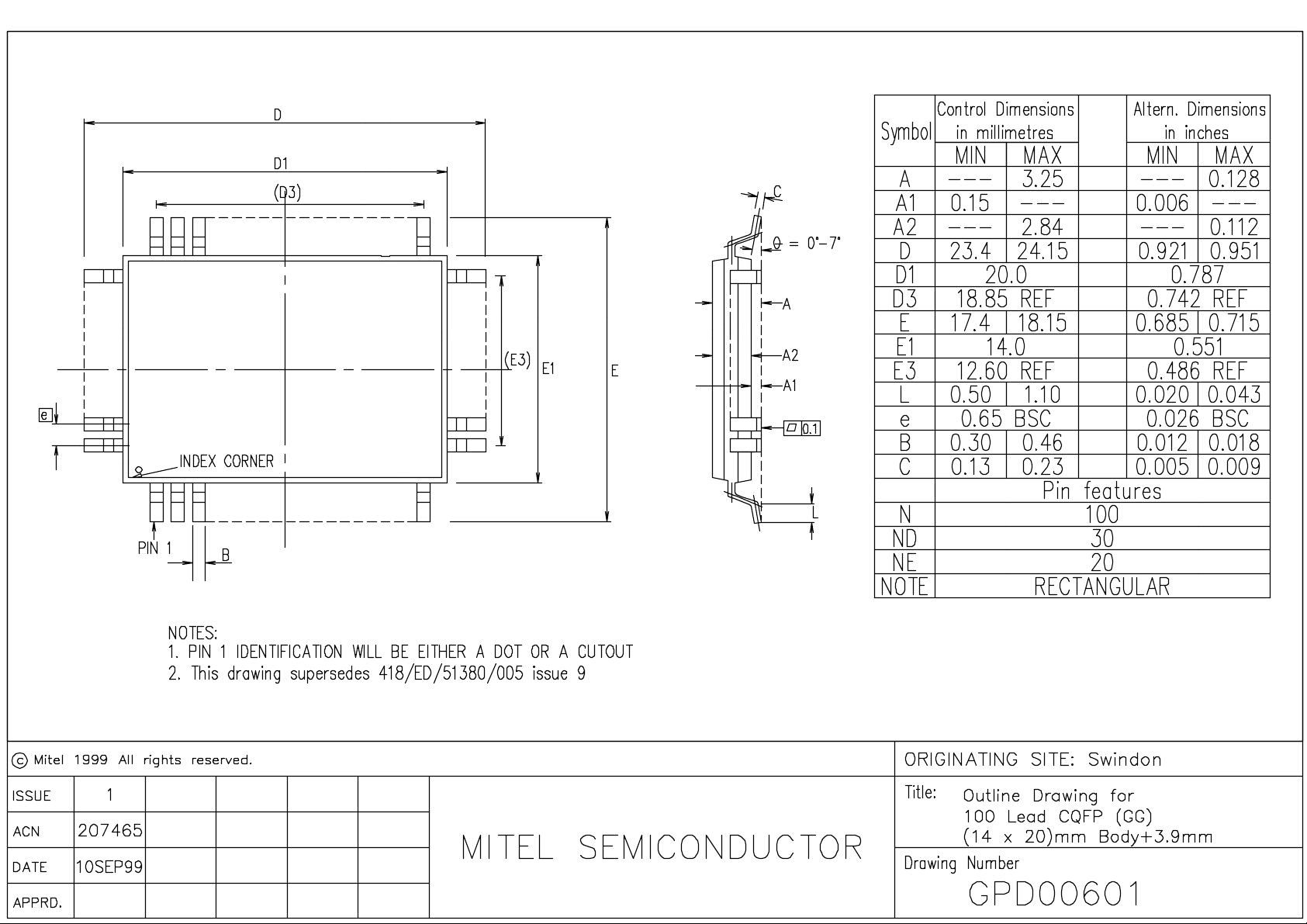
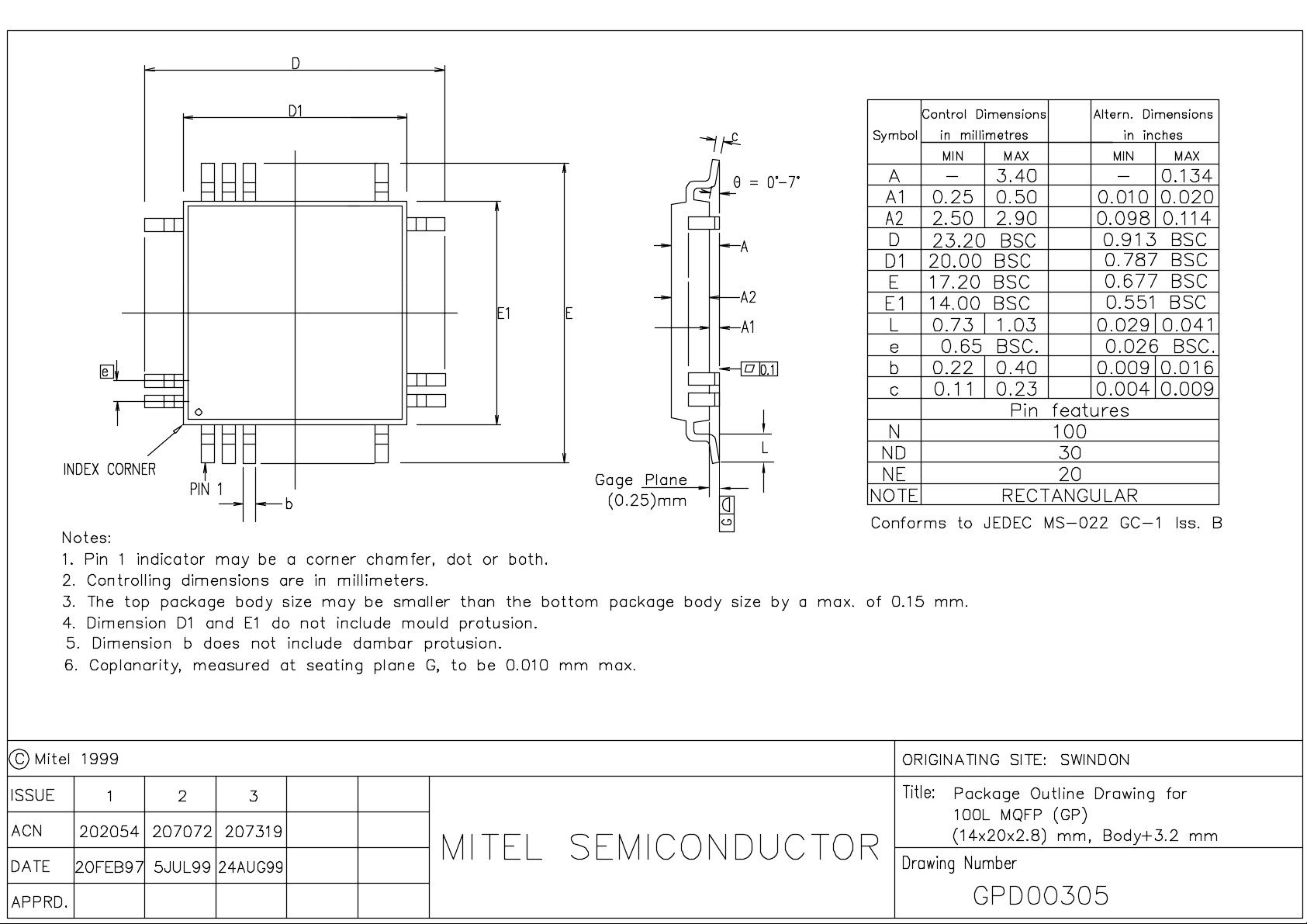
VP2614 CG GPFR (Commercial - plastic QFP package)
9
Page 10
Page 11
Page 12

http://www.mitelsemi.com
World Headquarters - Canada
Tel: +1 (613) 592 2122
Fax: +1 (613) 592 6909
North America Asia/Pacific Europe, Middle East,
Tel: +1 (770) 486 0194 Tel: +65 333 6193 and Africa (EMEA)
Fax: +1 (770) 631 8213 Fax: +65 333 6192 Tel: +44 (0) 1793 518528
Fax: +44 (0) 1793 518581
Information relating to products and services furnished herein by Mitel Corporation or its subsidiaries (collectively “Mitel”) is believed to be reliable. However, Mitel assumes no
liability for errors that may appear in this publication, or for liability otherwise arising from the application or use of any such information, product or service or for any infringement of
patents or other intellectual property rights owned by third parties which may result from such application or use. Neither the supply of such information or purchase of product or
service conveys any license, either express or implied, under patents or other intellectual property rights owned by Mitel or licensed from third parties by Mitel, whatsoever.
Purchasers of products are also hereby notified that the use of product in certain ways or in combination with Mitel, or non-Mitel furnished goods or services may infringe patents or
other intellectual property rights owned by Mitel.
This publication is issued to provide information only and (unless agreed by Mitel in writing) may not be used, applied or reproduced for any purpose nor form par t of any order or
contract nor to be regarded as a representation relating to the products or services concerned. The products, their specifications, services and other information appearing in this
publication are subject to change by Mitel without notice. No warranty or guarantee express or implied is made regarding the capability, performance or suitability of any product or
service. Information concerning possible methods of use is provided as a guide only and does not constitute any guarantee that such methods of use will be satisfactory in a specific
piece of equipment. It is the user’s responsibility to fully determine the performance and suitability of any equipment using such information and to ensure that any publication or
data used is up to date and has not been superseded. Manufacturing does not necessarily include testing of all functions or parameters. These products are not suitable for use in
any medical products whose failure to perform may result in significant injury or death to the user. All products and materials are sold and services provided subject to Mitel’s
conditions of sale which are available on request.
M Mitel (design) and ST-BUS are registered trademarks of MITEL Corporation
Mitel Semiconductor is an ISO 9001 Registered Company
Copyright 1999 MITEL Corporation
All Rights Reserved
Printed in CANADA
TECHNICAL DOCUMENTATION - NOT FOR RESALE
 Loading...