

Page 1
VP2615
VP2615
H.261 Decoder
Supersedes January 1996 edition, DS3479 - 3.0 DS3479 - 4.0 June 1996
FEATURES
■ Inputs run length coded transform data
■ Outputs 8 bit pixels in YUV block format
■ Up to full CIF resolution and 30 Hz frame rates
■ Supports motion compensation with up to 15 pixel
movement
■ On chip frame store controller
■ 100 pin QFP package
ASSOCIATED PRODUCTS
■ VP510 Colour Space Converter
■ VP520S Three Channel Video Filter
■ VP2611 Integrated H261 Encoder
■ VP2612 Video Multiplexer
■ VP2614 Video Demultiplexer
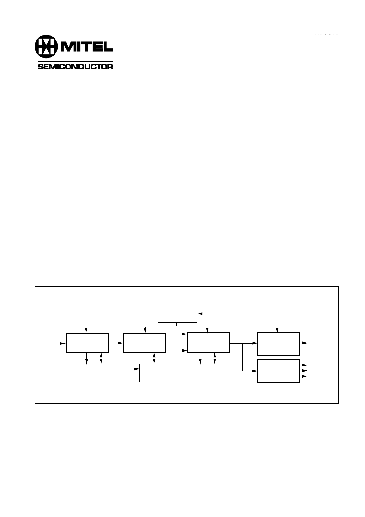
DESCRIPTION
The VP2615 decoder forms part of a chip set for use in
video conferencing and video telephony applications. It
conforms to the CCITT H261 standard, and will decode data
coded with full or quarter CIF resolution at frame rates up to 30
Hz.
It accepts run length coded coefficients which have already
been error corrected and Huffman decoded, and produces
multiplexed YUV data in macro block format after a pipeline
delay of two MacroBlocks. As shown in Figure 1, other devices
in the chip set then convert this data into full resolution,
component or composite, video.
The incoming run length coded data is converted to
individual coefficient values in the correct order. Data
reconstruction is then performed on a block by block basis by
multiplying the quantized coefficients with the original
quantization value, and then applying the inverse cosine
transform. In the inter frame mode this data is then added to
the motion compensated block from the previous frame. This
block can be passed through a low pass filter when required.
A frame store controller produces addresses which allow the
best fit block to be read from the frame store, and which also
allow the store to be updated with reconstructed data. Refresh
cycles are generated when necessary.
H261
BIT
STREAM
VP2614
VIDEO DEMUX
RECEIVE
BUFFER
32K X 8
RLC
DATA
SYSTEM
ADR
VP2615
VIDEO
DECODER
CIF FRAME
STORE
128K X 16
CONTROLLER
FRMOUT
MACRO
BLOCK
DATA
ADR
INTERFACE
VP520
3 CHANNEL
VIDEO FILTER
TWO CIF
FRAME STORES
256K X 16
Fig 1 : Typical Video Conferencing Receiver
USER
DATA
Y/CR/CB
VP530
NTSC/PAL
ENCODER
VP510
COLOUR SPACE
CONVERTER
COMP
NTSC/PAL
R G B
OUTPUTS
1
Page 2
VP2615
PIN DESCRIPTIONS
DIN7:0 This port is used to input quantised transform
data and control information. Its function is
determined by DMODE3:0. Data is clocked in
on the rising edge of DCLK.
DMODE3:0 This input controls the function of DIN7:0. Data
is clocked in on the rising edge of DCLK.
DCLK This signal is used to strobe in data at the DIN
and DMODE inputs. DCLK can effectively be
disabled by inputting a WAIT STATE on
DMODE. DCLK must be derived by dividing
SYSCLK with an integer greater than one.
YUV7:0 This bus outputs pixel data in YUV block format
at quarter SYSCLK frequency.
VPIX This synchronous output pulses high for two
SYSCLK periods when valid pixel data appears
at the YUV port. It remains low when inactive.
MBOUT This synchronous output goes high on the first
cycle of a new MacroBlock and stays high until
the final pixel of that MacroBlock has been
output. At the end of the MacroBlock MBOUT
goes low until a new MacroBlock begins.
FRMOUT This synchronous output goes high to indicate
a new Frame is about to begin at the YUV port.
It remains high till the last pixel is output. Then,
FRMOUT goes low until a new Frame starts.
FS15:0 Data bus for reading and writing to the external
DRAM frame store.
RW1 Read/Write control for the external DRAM 1.
RW2 Read/Write control for the external DRAM 2.
OE1 Output Enable control for external DRAM 1
or ADR8 if 256K DRAM's in use.
OE2 Output Enable control for external DRAM 2
N/C if 256k DRAMs in use.
CBUS7:0 Bi-directional data bus for use by a microproc-
essor. Data and instructions are clocked on and
off the chip on the rising edge of CSTR.
CSTR This input strobes the data in and out of the
CBUS port.
CEN When this pin is low the CBUS port
can be used to input or output data.
CADR When high this signal defines CBUS as data,
and when low as an instruction.
SYSCLK System clock, run at 27MHz maximum.
SYSCLK must remain high for 35% to 65% of
each cycle. All internal clocks are derived from
this clock.
RESET Active low reset. Must be held low for at least
2048 cycles on power up. If RESET is used
during operation, all previous frame data will be
lost.
TCK Test clock for JTAG
ADR7:0 Address bus controlling the external DRAM
frame store.
RAS Row Address Strobe controlling the external
DRAM frame store.
CAS Column address strobe controlling the external
DRAM frame store.
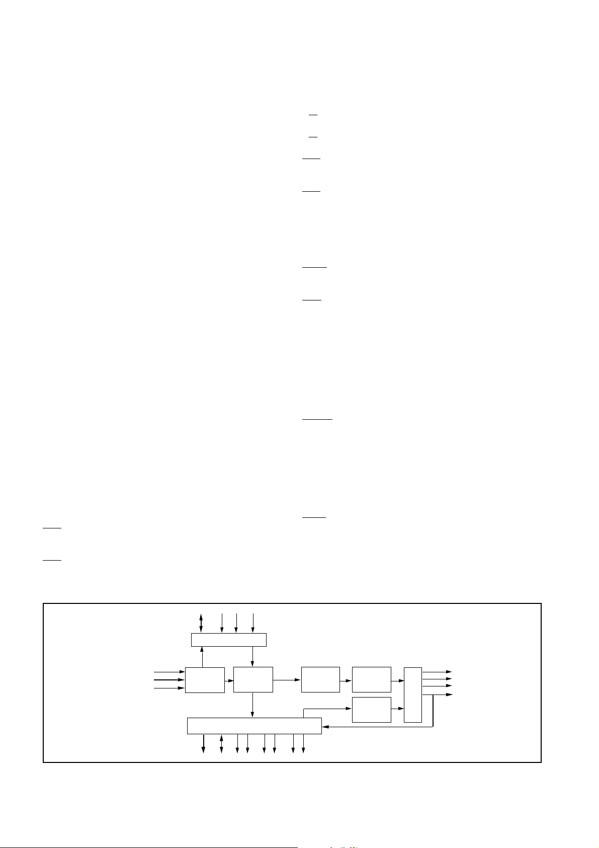
CBUS[7:0] CSTR CADR CEN
CONTROL I/F
DCLK
DIN[7:0]
DMODE[3:0]
INPUT
CONTROLLER
ADR[7:0] FS[15:0] OE1 OE2 RW1 RW2 RAS CAS
2
RUN LENGTH
DECODE &
INV ZIG ZAG
FRAME STORE CONTROLLER
Fig 2 : Simplified Block Diagram
TMS Test mode select for JTAG (Internally pulled high).
TRST JTAG reset pin (Internally pulled high).
TDI Input JTAG test data (Internally pulled high).
TDO Output JTAG test data.
NOTE:
"Barred" active low signals do not appear with a bar in the
main body of the text.
INVERSE
QUANTIZATION
INVERSE
DCT
LOW PASS
FILTER
ADD
FRMOUT
MBOUT
VPIX
YUV[7:0]
Page 3
OPERATION OF MAJOR BLOCKS
-
-
-
-
-
-
-
VP2615
Run Length Decode
This block converts the run length coded data into 64
individual coefficient values, inserting zero value coefficients
where required. It then re-orders these 8 bit quantized DCT
coefficients from the zig zag arrangement into normal 8 x 8
format.
Inverse Quantise
This circuit reconstructs the 12 bit DCT coefficients from
the 8 bit quantized coefficients using the 5 bit Quantization
Value. This is performed using the following formulae.
If QUANT is odd :
REC = QUANT*(2*LEVEL+1) : LEVEL > 0
REC = QUANT*(2*LEVEL-1) : LEVEL < 0
If QUANT is even :
REC = QUANT*(2*LEVEL+1)-1 : LEVEL > 0
REC = QUANT*(2*LEVEL-1)+1 : LEVEL < 0
For Intra coded DC coefficients :
REC = 8*LEVEL
except if LEVEL=255 when REC=1024
If LEVEL=0 then REC=0 in all cases.
The reconstructed values (REC) are passed through a
clipping circuit in case of arithmetic overflow.
Inverse DCT
This circuit performs an Inverse Discrete Cosine Transform on an 8x8 block of 12 bit coefficients outputting 9 bit
signed pixel data. This IDCT fully meets the CCITT specification.
Frame Store Interface
The whole of the previous picture is stored in either two
external 64K x 16 DRAMs, or in a single 256 k x 16 DRAM, or
in four 256K x 4 DRAM's. A bit in the user defined Input Set Up
Data determines whether 64K or 256K DRAM's are to be
used. In the latter case, use OE1 as ADR8, RW1 as R/W and
do not connect RW2 and OE2.Table 1 specifies the worst case
maximum and minimum times which must be achieved by the
DRAM for correct operation with the VP2615. Times in the
DRAM specification must be less than or equal to the times
stated.
The Frame Store Interface manages all read and write
operations to these DRAM's. During the course of each
MacroBlock, the "Best Fit" MacroBlock is read from the
DRAMs and the fully processed MacroBlock is written back. In
this way, the previous frame is continually updated. The
DRAM controller also takes care of refresh for the DRAMs.
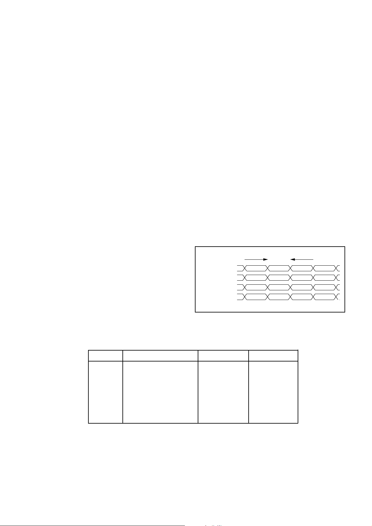
Figure 3 illustrates the effects of the pipeline delays
through the device; whilst macro block 3 is being input the
previous macroblock (2) is being decoded and needs the
equivalent macroblock from the previous frame to be read
from the frame store. At the same time macroblock 1, which
has already been decoded, is being written to the frame store
Minimum of
2048 cycles
DIN Input
Frame Store Read
Frame Store Write
YUV Output
MB3 MB4 MB5 MB6
MB2 MB3 MB4 MB5
MB1 MB2 MB3 MB4
MB1 MB2 MB3 MB4
Fig 3 : MacroBlock Pipelining
SYMBOL PARAMETER MINIMUM MAXIMUM
t RAC Access time from RAS
t CAC Access time from CAS
105ns or under
25ns or under
t RP RAS precharge time 50ns or under
t CP CAS precharge time 15ns or under
t RAS RAS pulse width 90ns or under
t CAS CAS pulse width 50ns or under
t REF Time to refresh 256 rows
0.25ms or over
N.B. All times are quoted assuming 27MHz operation. For lower clock
frequencies increase the above values proportionately.
Table 1. External DRAM Timing Requirements
3
Page 4
VP2615
for use in the next frame and is also available on the output
pins.
Loop Filter
The best matched block from the search window in the
previous frame can be passed through a low pass filter to
reduce block boundary effects. The filter uses a simple [1 2 1]
characteristic in both horizontal and vertical dimensions as
laid down in the H261 Specification, on the macroblock
boundaries [010] is used. An instruction input at the DIN port
defines whether the filter should be used or not.
Reconstruction Adder
In Inter Mode, the IDCT data is added to the best fit block
from the previous frame store. In Intra Mode, the IDCT data is
added to zero. After the adder, the sign bit is removed from the
result to give 8 bit pixels. Clipping circuits ensure that any
pixels with values exceeding 255 are clipped to 255 and any
with negative values are clipped to zero (such values are
possible due to quantization effects).
OPERATION OF INTERFACES
DIN Input Port
The DIN port provides a glueless interface to the VP2614
Video Demultiplexer, from which it will accept run length
coded transform data and control information. The general
purpose nature of the interface will, however, allow other
sources of macroblock data to be used.
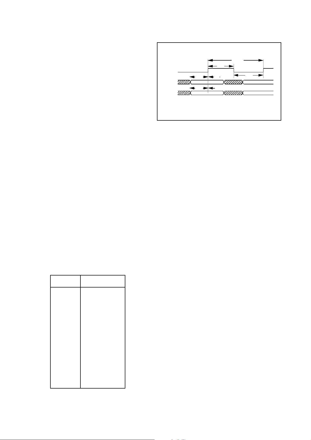
Data on the input bus is defined by means of the signals
DMODE3:0, and is strobed in with the DCLK signal which is
provided by the VP2614 and derived from SYSCLK. Set up
and hold times with respect to the rising edge of DCLK are
given in Figure 4. If DCLK is a continuous strobe, then the
WAIT state defined by DMODE 3:0 should be used to disable
any clocking actions. If preferred DCLK can alternatively be
DMODE3:0 FUNCTION
0000
0001
0010
0011
0100
0101
0110
0111
1000
1001
1010
1011
1100
1101
1110
1111
GOB Number
MB Number
Control Decisions
Quant Value
Horizontal MV
Vertical MV
Coded Blk Pattern
Sub-Block No
Zero Run Count
RLC Coefficient
Not used
Not used
Not used
Not used
Not used
Wait State
SCLK/2
20ns
DCLK
DIN7:0
DMODE3:0
10ns 2ns
10ns
N.B. All timings given are minimum values.
Fig 4 . DIN Port Timing
2ns
20ns
used as a strobe which is only present when data is valid and
action is needed. In this case WAIT states are not strictly
necessary.
The VP2615 always expects to receive a complete video
frame of data, even if error conditions have occurred in the demultiplexer. Skip Picture or Fixed Macroblocks should be
supplied if necessary once a frame has started. With the latter,
decoded data from the previously stored frame will be produced by the VP2615.
The asynchronous interface will allow the use of other
video de-multiplexers, as long as the protocol defined by
DMODE3:0 is observed. This protocol is defined below, and
summerized in Table 2.
Control Decisions : This byte must always be the first in the
sequence since it resets the internal control logic. It
defines which control decisions were taken when coding
the forthcoming MacroBlock. A high on DIN 0 indicates a
Fixed Macro Block (ie no change since the previous
frame), and a high on DIN1 indicates that Inter coding was
used. Similarly a high on DIN2 indicates that the
MacroBlock was filtered, a high on DIN3 indicates that
Motion Compensation was used. and a high on DIN6
indicates that SKIP PICTURE is in effect. In the latter case
the VP2615 will cease processing until SKIP PICTURE is
reversed by writing a new Control Decisions byte. Whilst
SKIP PICTURE is active, no further data will be output
from the YUV port. SKIP PICTURE effectively resets the
VP2615, and the next MacroBlock input should be the first
of a new frame. Since the frame store will not be updated
then the system should ensure that an Intra coded picture
is sent as soon as possible.
GOB Number: The correct GOB number is required for every
macro block in that group. (DIN3 is MSB).
MB Number: Each macroblock in a group requires an identi-
fication number. (DIN5 is MSB).
Coded Blk Pattern: This byte is defined in the H.261
Specification and is used to indicate which sub blocks
contain non zero coefficients. It is produced by the encoder
but is not used by the VP2615, and if provided will be
ignored. The sub block numbering sequence is actually
used to indicate blocks with zero coefficients.
Table 2 . DIN Mode Functions
Quant Value: This input represents the quantization value
4
Page 5

(between 2 and 62 with DIN4 as MSB ), which has been
Y
V
ROBLOCK
CK
used for this macroblock. If no new value is provided for a
macroblock then the old value is re-used.
Horizontal MV: This input (on DIN4:0 ) represents the horizon-
tal component of the motion vector. It must always be
provided when motion compensated Inter coding is in use.
Vertical MV: This input (On DIN4:0) represents the vertical
component of the the motion vector. It must always be
provided when motion compensated Inter coding is in use.
SYSCLK
FRMOUT
MBOUT
VPIX
YUV
VP2615
Pixel 0 Pixel 1 Pixel 2 Pixel 383
Sub Blk No: Each macroBlock contains 6 Sub-blocks, num-
bered 1 through 6. The corresponding binary value should
be provided on DIN2:0, before the RLC coefficients of that
Sub-Block appear. If a Sub-Block contains no coefficients,
then its number need not be provided at all, or it can be
immediately followed by the next sub block number without any intermediate coefficient values. Even though zero
valued sub blocks can simply be ignored in this way, a
2048 clock delay between new macroblocks must still be
maintained by the video de-multiplexer.
Zero Run Count: The number of zero valued coefficients
preceding the (non-zero) RLC coefficient is defined by this
input. DIN 6 and 7 are not used, with the value between 0
and 63 defined by DIN5:0.
RLC Coefficient: This input defines the value of the run length
coded coefficient. It will always be a non-zero value
Wait State: This mode should be used on any cycle where no
data is being input at the DIN port. Wait States can be
SUBBLOCK ORDER WITHIN MAC
1 2
5
3 4
PIXEL ORDER WITHIN SUBBLO
00 01 02 03 04 05 06 07
08 09 10 11 12 13 14 15
16 17 18 03 20 21 22 23
24 25 26 27 28 29 30 31
32 33 34 35 36 37 38 39
40 41 42 43 44 45 46 47
48 49 50 51 52 53 54 55
56 57 58 59 60 61 62 63
Fig 5 : Ordering of Pixels within MacroBlock
U
19
6
Fig 6 : YUV Port Timing
inserted between any other instructions as required.
Any undefined bits in the above descriptions may be made
high or low as desired.
The first information supplied for a macroblock should be
that contained within the Control Decisions byte. Receipt of
this instruction resets the internal cycle counter for that
MacroBlock. Although some Macro Blocks may contain no
data, the VP2615 requires that at least the Control Decisions,
GOB Number and Macro Block Number be supplied by the
de-multiplexer ( in that order ). All other side information, which
is to be provided for a non zero block, must then be supplied
before any sub block data can be accepted. GOB's and
Macroblocks must be supplied in the correct sequence, but
sub blocks within a macroblock can be in any order. The
VP2615 does not need to be explicitly informed that the last
coefficient has been received within a sub-block. It will wait for
a new sub-block number, or a new Macroblock Control Decision Byte, before processing the previous sub-block since it
then knows that the sub block is complete.
At least 2048 SYSCLK cycles must separate the start of
one Macro Block (identified by receipt of the Control Decisions
byte) from the start of the following Macro Block. There are,
however, no specific restrictions on the timing of Sub-Blocks
within the MacroBlock. The minimum gap between incoming
macroblocks is needed for internal processing and also for the
time to output 384 decoded values at one quarter the SYSCLK
frequency.
The VP2615 contains two complete macro block buffers in
its input circuitry, which swap on the completion of the processing and outputting of the results. Whilst one is used internally
the other can be loaded with a new macroblock. It essentially
is a macroblock processor and produces the decoded outputs
for a macroblock after two macroblock pipeline delays. When
it is no longer supplied with macroblock inputs then the
pipeline stalls and does not flush out. Thus two macroblocks
from a new picture are needed to produce the decoded
outputs from the last two macroblocks in a previous picture.
YUV Output Port
Decoded pixel data is presented at the YUV port in
standard macroblock format at quarter SYSCLK frequency
(6.75MHz max), and in the macroblock order presented at the
input. Since the VP2615 always expects a complete picture's
worth of GOB's and macroblocks ( unless Skip Picture is sent
by the video de-mux ), then it will always produce a complete
5
Page 6

VP2615
WRITING DATA ONTO THE CBUS:
WRITING DATA FROM THE CBUS:
This diagram shows a typical instruction and associated data field being written to the device.
10ns
CEN
CADR
CSTR
CBUS
I/P
20ns
20ns
20ns
20ns
20ns
20ns
20ns
20ns
INSTRUCTION
10ns
10ns
10ns
10ns
10ns
20ns
20ns
20ns
20ns
20ns
DATA IN
READING INFORMATION ON CBUS :
This diagram shows a typical instruction and associated data field being read from the device.
CEN
CADR
CSTR
CBUS
20ns
20ns
20ns
20ns
INSTRUCTION
10ns
10ns
10ns
Th
20ns
50ns
10ns
20ns
20ns
20ns
20ns
*
*
10ns
10ns
10ns
10ns
10ns
20ns
DATA OUT
*
If Th is less than 5 ns then CBUS may be driven by the VP2615until CEN going high eventually turns off
the drivers. It will not prevent correct data being read when CEN again goes active
N.B. All timings shown are minimum values except those marked * which are maximums.
Fig 7 : CBUS Timing
coded picture. As explained in the previous section, however,
it requires to be supplied with two macroblocks from the next
picture before a complete frame is fully decoded. The standard macroblock internal configuration is shown in Figure 5.
Output timing is shown in Figure 6. VPIX is toggled high
each time a valid pixel is available at the output pins, and
remains low when no pixel data is output. MBOUT is used to
define the boundaries between MacroBlocks, but is not used
when the device is directly connected to the VP520. The
Frame Ready Output nominally goes high on the same SYSCLK
edge as the first MBOUT goes high, and returns low when the
last MBOUT goes low. This will actually be after two macroblocks from the next frame have been supplied as inputs, but
this gap will not effect the operation of the VP520 which
converts macro block data to full resolution line data. The first
VPIX strobe produced after MBOUT goes high, will go high
after two SYSCLK periods, with the data being valid for two
SYSCLK periods either side of this edge. These delays are
subject to internal differential delays and will not be precise
clock period delays.
CBUS Control Port
The CBUS control port is used to input control and setup
information and also to output status information. In order to
save on pin count, a microprocessor driving this port is
required to execute two I/O instructions in order to transfer a
single byte of information to or from the device. The first
transfer is always a write operation, with a low level on the
single address line which is used by the interface. Data on the
bus then defines the instructions listed in Table 3. The second
transfer can be a read or write operation as necessary, but the
address line must then be high with the set up time given in
Figure 7.
In addition to the single addresss line (CADR), data
transfers use a control strobe (CSTR) which is only effective
6
Page 7

VP2615
CBUS3:0 INSTRUCTION
0000
0001
0010
0011
0100
0101
0110
0111
1000
1001
1010
1011
1100
1101
1110
1111
when a chip enable is present (CEN). Detailed timing information is given in Figure 7, and when writing data or instructions
to the VP2615 the set up and hold times which are referenced
to the rising edge of CSTR must be maintained.
When a write instruction has been defined CADR should
be pulled high, valid data presented to CBUS7:0 and then
strobed in using CSTR. Other system I/O transfers can occur
between defining a write operation and supplying the data to
be written, assuming CEN is not active during those other
transfers. If CSTR does not go active because of I/O transfers
to other devices, then CEN can remain active low between the
instruction and data.
When a read instruction has been specified the requested
data will then be output on CBUS7:0 after the access time
specified from CEN going low, assuming that CADR was
already high. Otherwise the data will become valid after the
access time specified from CADR going high after CEN was
low. Note that in the data read phase CADR must always go
high before CSTR goes high, with the set up time specified.
When CEN goes high, or CADR goes low, the CBUS will go
high impedance after the delay specified.
Note that the access times under the conditions given
above are only true when the gap between CSTR going high
in the instruction phase, and CEN going low in the data phase,
is greater than the minimum specified in figure 7.
Only CBUS3:0 are used to define an instruction. The
remaining bits, CBUS7:4, should be pulled low. The instructions are listed in Table 3 but are described below in greater
detail;
Input Setup Data: This instruction performs several functions,
the details being specified in the data field following this
instruction. If CBUS0 is high, the device will operate in
QCIF mode, otherwise in full CIF mode. If CBUS6 is high,
then the device will be configured to use 256K word
DRAM's, otherwise it will assume two 64K word DRAM's.
Overide internal clock doubler
Table 3: CBUS Instructions
Unassigned
Unassigned
Unassigned
Unassigned
Input Setup Data
Unassigned
Reserved
Reserved
Output GOB Number
Output MB Number
Unassigned
Output Control Decisions
Output Setup Data
Unassigned
Unassigned
All CBUS inputs not defined above must be pulled low
during the set up definition phase and the D/R7:0 bus must
not be active. On reset the defaults are 64k DRAMs and
full CIF mode. Note that if macroblocks have been
received, and a CIF/QCIF mode change is made, then a
reset is needed. At the the system level the EVT signal
from the de-mux can be used to instigate the controller into
reading PTYPE, thus detecting a CIF/QCIF change and
forcing a software reset.
Output GOB number: This instruction will make the VP2615
output the GOB Number associated with the data currently
being output at the YUV port. The number will appear on
CBUS3:0. CBUS7:4 are not used (always low).
Output MB Number: This instruction will make the VP2615
output the Macroblock Number associated with the data
currently being output at the YUV port. The number will
appear on CBUS5:0. If CBUS6 is low, this indicates that
the MacroBlock number has just changed or is about to
change, and is thus not reliable.
Output Control Decisions : This instruction will make the
VP2615 output control information received through the
DIN port. CBUS0 shows whether the MacroBlock currently
being output was Inter or Intra coded (0=Intra). CBUS1
shows whether Motion Compensation was used (1=MC
used). CBUS3 will be high if the MacroBlock was passed
through the Loop Filter. If CBUS6 is high, this indicates that
SKIP PICTURE is currently active.
JTAG Test Interface
The VP2615 includes a test interface consisting of a
boundary scan loop of test registers placed between the pads
and the core of the chip. The control of this loop is fully JTAG/
IEEE 1149-1 1990 compatible. Please refer to this document
for a full description of the standard.
The interface has five dedicated pins: TMS, TDI, TDO,
TCK and TRST. The TRST pin is an independent reset for the
interface controller and should be pulsed low, soon after
power up; if the JTAG interface is not to be used it can be tied
low permanently. The TDI pin is the input for shifting in serial
instruction and test data; TDO the output for test data. The
TCK pin is the independent clock for the test interface and
registers, and TMS the mode select signal.
TDI and TMS are clocked in on the rising edge of TCK, and
all output transitions on TDO happen on its falling edge.
Instructions are clocked into the 8 bit instruction register
(no parity bit) and the following instructions are available.
Instruction Register Name
( MSB first )
11111111 BYPASS
00000000 EXTEST (No inversion)
01000000 INTEST
XX001011 SAMPLE/PRELOAD
7
Page 8

VP2615
TCK
TCK
TMS toTCK timing
TDI to TCK timing
Chip i/p to TCK timing
Signal
Tsu
Thd
Signal
Tprop
Tsu Thd Tprop
15
15
15
TCK to TDO timing
5
5
5
20
Fig 8. Typical JTAG Interface timing
Timing details ( minimums ) for the JTAG control signals
are shown in Figure 8. The maximum TCK frequency is 5 MHz.
The positions of the test registers in the boundary loop,
and their corresponding functional names, are detailed in
Table 4. Note that any internal signals controlling the impedance of a bus also have associated registers, even though
they are not normally available to the user. These are listed
as TRI in Table 4.This register order will determine the serial
data stream for JTAG testing. The signal DHZ will, if loaded
with a logic '1', force all the outputs to a high impedance state.
All bus output enables are invoked through the INTEST
instruction.
PAD
DHZ
CADR
CEN
CSTR
CBUS0
CBUS
CBUS0
CBUS1
CBUS1
CBUS2
CBUS2
CBUS3
CBUS3
SYSCLK
CBUS4
CBUS4
CBUS5
CBUS5
CBUS6
CBUS6
CBUS7
CBUS7
DMODE0
DMODE1
RESET
DCLK
DMODE2
DMODE3
DIN0
DIN1
DIN2
DIN3
DIN4
DIN5
DIN6
DIN7
FS15
FS
FS15
FS14
FS14
FS13
FS13
FS12
FS12
FS11
FS11
TYPE
TRI
IN
IN
IN
OP
TRI
IP
OUT
IN
OUT
IN
OUT
IN
IN
OUT
IN
OUT
IN
OUT
IN
OUT
IN
IN
IN
IN
IN
IN
IN
IN
IN
IN
IN
IN
IN
IN
IN
IN
TRI
OUT
IN
OUT
IN
OUT
IN
OUT
IN
OUT
REG NO
93
92
91
90
89
88
87
86
85
84
83
82
81
80
79
78
77
76
75
74
73
72
71
70
69
68
67
66
65
64
63
62
61
60
59
58
57
56
55
54
53
52
51
50
49
48
47
PAD
FS10
FS10
FS9
FS9
FS8
FS8
FS7
FS7
FS6
FS6
FS5
FS5
FS4
FS4
FS3
FS3
FS2
FS2
FS1
FS1
FS0
FS0
ADR7
ADR6
ADR5
ADR4
ADR3
ADR2
ADR1
ADR0
RW1
RW2
DE1
DE2
RAS
CAS
MBOUT
FRMOUT
VPIX
YUV0
YUV1
YUV2
YUV3
YUV4
YUV5
YUV6
YUV7
TYPE
IN
OUT
IN
OUT
IN
OUT
IN
OUT
IN
OUT
IN
OUT
IN
OUT
IN
OUT
IN
OUT
IN
OUT
IN
OUT
OUT
OUT
OUT
OUT
OUT
OUT
OUT
OUT
OUT
OUT
OUT
OUT
OUT
OUT
OUT
OUT
OUT
OUT
OUT
OUT
OUT
OUT
OUT
OUT
OUT
REG NO
46
45
44
43
42
41
40
39
38
37
36
35
34
33
32
31
30
29
28
27
26
25
24
23
22
21
20
19
18
17
16
15
14
13
12
11
10
9
8
7
6
5
4
3
2
1
0
Table 4. Pin and JTAG Test Registers
10
11
12
13
14
15
16
17
18
19
20
GND
1
N/C
2
FS3
3
FS4
4
GND
5
FS5
6
FS6
7
VDD
8
FS7
9
FS8
FS9
GND
FS10
VDD
FS11
FS12
FS13
FS14
FS15
GND
21
22
23
24
25
26
27
28
29
30
31
32
33
34
35
36
37
38
39
40
DIN7
DIN6
DIN5
DIN4
VDD
DIN3
DIN2
DIN1
N/C
GND
DIN0
DMODE3
DMODE2
VDD
DCLK
GND
RESET
DMODE1
DMODE0
CBUS7
41
42
43
44
45
46
47
48
49
50
51
52
53
54
55
56
57
58
59
60
CBUS6
CBUS5
CBUS4
VDD
SYSCLK
GND
CBUS3
CBUS2
CBUS1
CBUS0
GND
N/C
CSTR
VDD
CEN
CADR
GND
TD1
TMS
TCLK
61
62
63
64
65
66
67
68
69
70
71
72
73
74
75
76
77
78
79
80
TRST
TD0
YUV7
YUV6
VDD
YUV5
GND
YUV4
YUV3
YUV2
YUV1
YUV0
VDD
VPIX
FRMOUT
GND
MBOUT
CAS
N/C
GND
81
82
83
84
85
86
87
88
89
90
91
92
93
94
95
96
97
98
99
100
RAS
OE2
OE1
GND
RW2
VDD
RW1
ADR0
ADR1
ADR2
ADR3
ADR4
ADR5
GND
ADR6
VDD
ADR7
FS0
FS1
FS2
Table 5. 100 Pin QFP Pin Assignment
8
Page 9

VP2615
ABSOLUTE MAXIMUM RATINGS [See Notes]
Supply voltage VDD -0.5V to 7.0V
Input voltage V
Output voltage V
Clamp diode current per pin IK (see note 2) 18mA
IN
OUT
Static discharge voltage (HBM) 500V
Storage temperature T
Ambient temperature with power applied T
S
-0.5V to VDD + 0.5V
-0.5V to VDD + 0.5V
-55°C to 150°C
AMB
NOTES ON MAXIMUM RATINGS
1. Exceeding these ratings may cause permanent damage.
Functional operation under these conditions is not implied.
2. Maximum dissipation for 1 second should not be exceeded,
only one output to be tested at any one time.
3. Exposure to absolute maximum ratings for extended periods may affect device reliablity.
4. Current is defined as negative into the device.
0°C to 70°C
Junction temperature 125°C
Package power dissipation 1000mW
STATIC ELECTRICAL CHARACTERISTICS Operating Conditions (unless otherwise stated)
Tamb = 0°C to +70°C VDD = 5.0v ± 5%
Characteristic
Output high voltage
Output low voltage
Input high voltage
Input low voltage
Input leakage current
Input capacitance
Output leakage current
Output S/C current
Symbol Value Units
10
Typ.
-
10
Max.
-
0.4
-
0.8
+10
+50
300
V
V
V
V
µA
pF
µA
mA
Min.
V
OH
V
OL
V
IH
V
IL
I
IN
C
IN
I
OZ
I
SC
2.4
2.0
-10
-50
Conditions
IOH = 4mA
IOL = -4mA
V
-1V for SYSCLK, DCLK
DD
GND < VIN < V
GND < V
VDD = Max
OUT
< V
DD
DD
ORDERING INFORMATION
VP2615 CG GH1R (Commercial - Plastic QFP power package)
9
Page 10

Page 11

http://www.mitelsemi.com
World Headquarters - Canada
Tel: +1 (613) 592 2122
Fax: +1 (613) 592 6909
North America Asia/Pacific Europe, Middle East,
Tel: +1 (770) 486 0194 Tel: +65 333 6193 and Africa (EMEA)
Fax: +1 (770) 631 8213 Fax: +65 333 6192 Tel: +44 (0) 1793 518528
Fax: +44 (0) 1793 518581
Information relating to products and services furnished herein by Mitel Corporation or its subsidiaries (collectively “Mitel”) is believed to be reliable. However, Mitel assumes no
liability for errors that may appear in this publication, or for liability otherwise arising from the application or use of any such information, product or service or for any infringement of
patents or other intellectual property rights owned by third parties which may result from such application or use. Neither the supply of such information or purchase of product or
service conveys any license, either express or implied, under patents or other intellectual property rights owned by Mitel or licensed from third parties by Mitel, whatsoever.
Purchasers of products are also hereby notified that the use of product in certain ways or in combination with Mitel, or non-Mitel furnished goods or services may infringe patents or
other intellectual property rights owned by Mitel.
This publication is issued to provide information only and (unless agreed by Mitel in writing) may not be used, applied or reproduced for any purpose nor form par t of any order or
contract nor to be regarded as a representation relating to the products or services concerned. The products, their specifications, services and other information appearing in this
publication are subject to change by Mitel without notice. No warranty or guarantee express or implied is made regarding the capability, performance or suitability of any product or
service. Information concerning possible methods of use is provided as a guide only and does not constitute any guarantee that such methods of use will be satisfactory in a specific
piece of equipment. It is the user’s responsibility to fully determine the performance and suitability of any equipment using such information and to ensure that any publication or
data used is up to date and has not been superseded. Manufacturing does not necessarily include testing of all functions or parameters. These products are not suitable for use in
any medical products whose failure to perform may result in significant injury or death to the user. All products and materials are sold and services provided subject to Mitel’s
conditions of sale which are available on request.
M Mitel (design) and ST-BUS are registered trademarks of MITEL Corporation
Mitel Semiconductor is an ISO 9001 Registered Company
Copyright 1999 MITEL Corporation
All Rights Reserved
Printed in CANADA
TECHNICAL DOCUMENTATION - NOT FOR RESALE
 Loading...